10 Channel Analog-To-Digital (ADC) Converter – 32bit
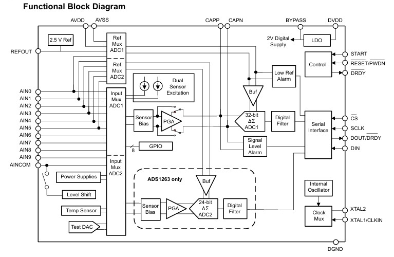
This is a low-noise, 32-bit, 38-kSPS, 10-channel (multiplexed), delta-sigma (ΔΣ) analog-to-digital converter (ADC) module. The project consists of highly integrated ADS1263 and includes a programmable gain amplifier (PGA), a 2.5-V low-drift voltage reference, an internal oscillator, dual-sensor excitation current sources (IDAC), several system-monitoring features, and an auxiliary 24-bit ΔΣ ADC.
This is a low-noise, 32-bit, 38-kSPS, 10-channel (multiplexed), delta-sigma (ΔΣ) analog-to-digital converter (ADC) module. The project consists of highly integrated ADS1263 and includes a programmable gain amplifier (PGA), a 2.5-V low-drift voltage reference, an internal oscillator, dual-sensor excitation current sources (IDAC), several system-monitoring features, and an auxiliary 24-bit ΔΣ ADC. The integrated features and excellent performance of the ADS1262 enable precision measurement of strain gauges, weight scales, pressure sensors, thermocouples, thermistors, and resistance temperature detectors (RTDs).
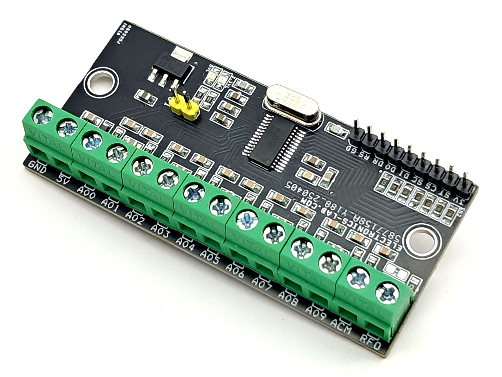
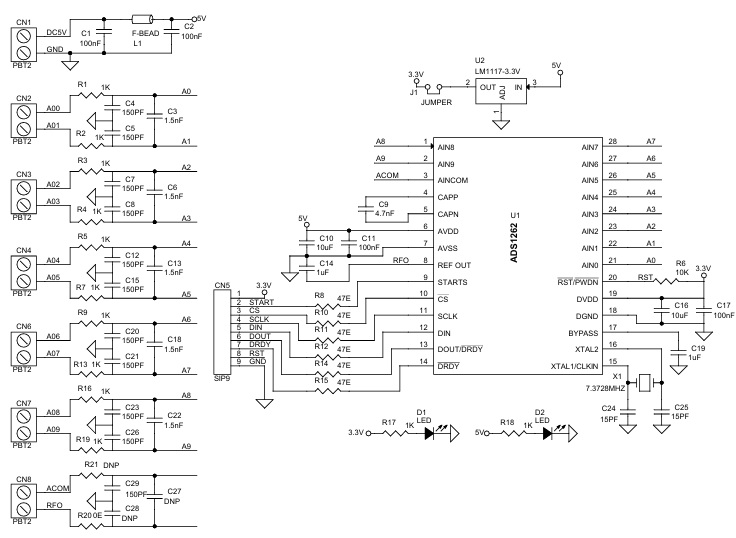
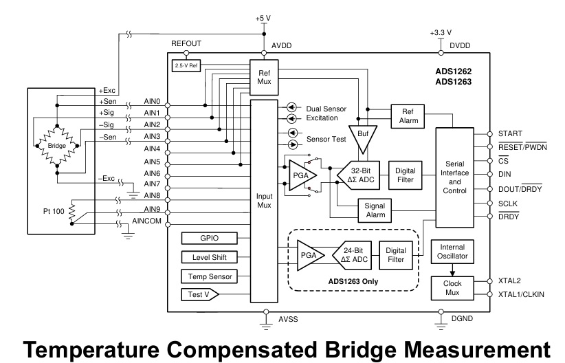
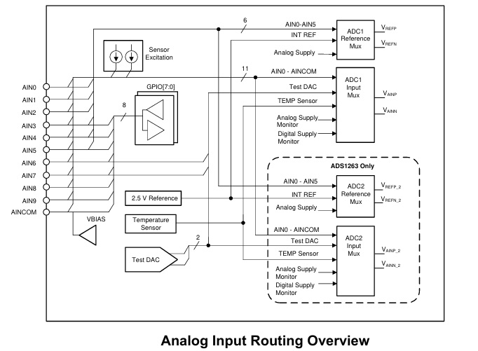
Analog Input Options the ADS1262 has a total of 11 analog input pins: AIN0 through AIN9 plus a common input, AINCOM. This design allows the ADS1262 to be configured for up to five differential input pairs, 10 single-ended inputs referenced to a common voltage, or a combination of single-ended and differential inputs. The flexible input multiplexer of the ADS1262 allows any two inputs to be selected for either the positive or negative ADC input. Any AINx pin can be used as a common input when measuring single-ended signals. However, AINCOM is specifically designed to serve this purpose because AINCOM can provide a bias voltage (level-shift function). This voltage biases floating sensors to help meet the common-mode voltage requirements of the AD1262 PGA. All ADC analog inputs are pinned out on the board. The supporting circuitry provides filtering and Ratiometric connections for a variety of sensors. Additionally, terminal block can be used for thermocouple inputs. Terminal block shows the connection and input filter for AINCOM.
Features
- Power Supply 5V DC (Analog Side)
- Power Supply 3.3V (Digital Side)
- On Board 5V, 3.3V LED
- Jumper to Combined 3.3V LDO to 3.3V Digital Supply
- Screw Terminals for Analog Inputs
- Header Connector for Digital Interface
- Precision, 32-bit, ΔΣ ADC
- Auxiliary 24-bit, ΔΣ ADC (ADS1263)
- Data rates: 2.5 SPS to 38400 SPS
- Differential input, CMOS PGA
- 11 multifunction analog inputs
- High-accuracy architecture: – Offset drift: 1 nV/°C– Gain drift: 0.5 ppm/°C– Noise: 7 nVRMS (2.5 SPS, gain = 32)– Linearity: 3 ppm
- 5-V internal voltage reference: – Temperature drift: 2 ppm/°C
- 50-Hz and 60-Hz rejection
- Single-cycle settled conversions
- Dual sensor excitation current sources
- Internal fault monitors
- Internal ADC test signal
- 8 general-purpose inputs/output
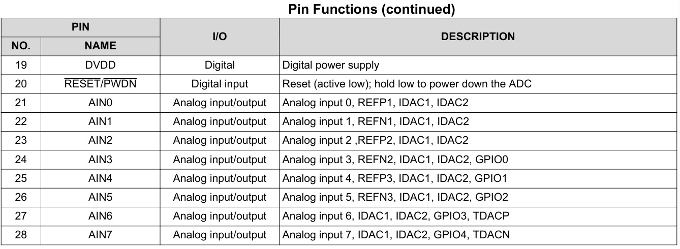
- PCB Dimensions 72.39 x 33.66 mm
As shown in the circuit Diagram, these devices feature 11 analog inputs that are configurable as either ten single-ended inputs, five differential inputs, or any combination, to either ADC1 or ADC2. Many of the analog inputs are multifunction as programmed by the user. The analog inputs can be programmed to the following extended functions:
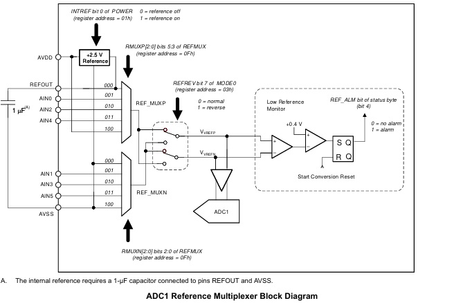
- Three external reference inputs: pins AIN0, AIN1, AIN2, AIN3, AIN4 and AIN5
- Two sensor excitation current source: all analog input pins
- Level shift (VBIAS): AINCOM pin
- Eight GPIO: pins AIN3, AIN4, AIN5, AIN6, AIN7, AIN8, AIN9, AINCOM
- Sensor breaks current source: all analog input pins
- Two test signal output: pins AIN6, AIN7
ADC Inputs
The ADS1262 has a flexible input multiplexer with 11 analog inputs. Any input can connect to the positive input and any input can connect to the negative input. The ADS1262 also includes an auxiliary, 24-bit ΔΣ ADC with an independent flexible input multiplexer to all input pins. Configure the inputs to provide either single-ended or differential input measurements.
IDAC Output
The ADS1262 provides dual-matched current sources (IDAC1 and IDAC2) for biasing of RTDs, thermistors, and other resistive-biased sensors. The IDACs can be independently programmed and can be connected to any analog input. Each IDAC output is programmable from 50 μA to 3000 μA. The ADC internal reference must be enabled for IDAC operation.
VBIAS Output
For single-supply operation, the level-shift function (VBIAS) can offset the common input voltage on AINCOM to a mid-supply voltage ([AVDD + AVSS] / 2).
Test DAC Output
An internal test DAC (TDAC) provides a known voltage to the ADC to diagnose the operation of the signal chain. The positive and negative TDAC voltages are output on AIN6 and AIN7, respectively. Do not load AIN6 and AIN7 when the test signals are enabled because the TDAC outputs are unbuffered.
GPIO
Eight inputs (AIN3 through AINCOM) are configurable as general-purpose input/outputs (GPIO). The GPIO voltages are referenced to the analog power supply (AVDD and AVSS) and therefore must use 5-V logic. Use the GPIOs to control external devices or to read external logic signals.
Analog Sensor Connections
The project is designed to easily interface with many types of analog sensors including weigh scales, strain gauge sensors, and analog temperature sensors. The following sections provide more detail for connecting and measuring temperature sensors, including thermocouples
The ADS1262 incorporate several functions that provide increased utility. The key integrated functions include:
- Low-drift voltage reference
- Dual, matched, sensor-excitation current sources (IDAC)
- Input-level-shift voltage
- Eight GPIOs
- Dual-sensor, bias current sources
- Low-noise, CMOS PGA with integrated signal fault detection
- Internal test signal source (TDAC)
- Temperature sensor
- Internal oscillator
- Three sets of buffered external reference inputs with low reference voltage alarm
Connection
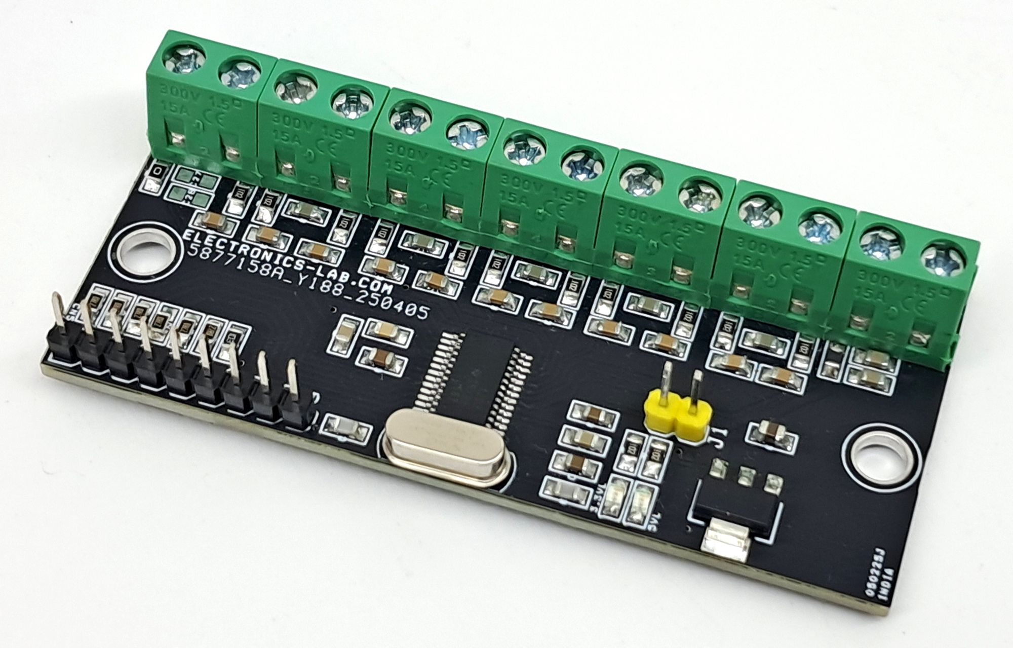
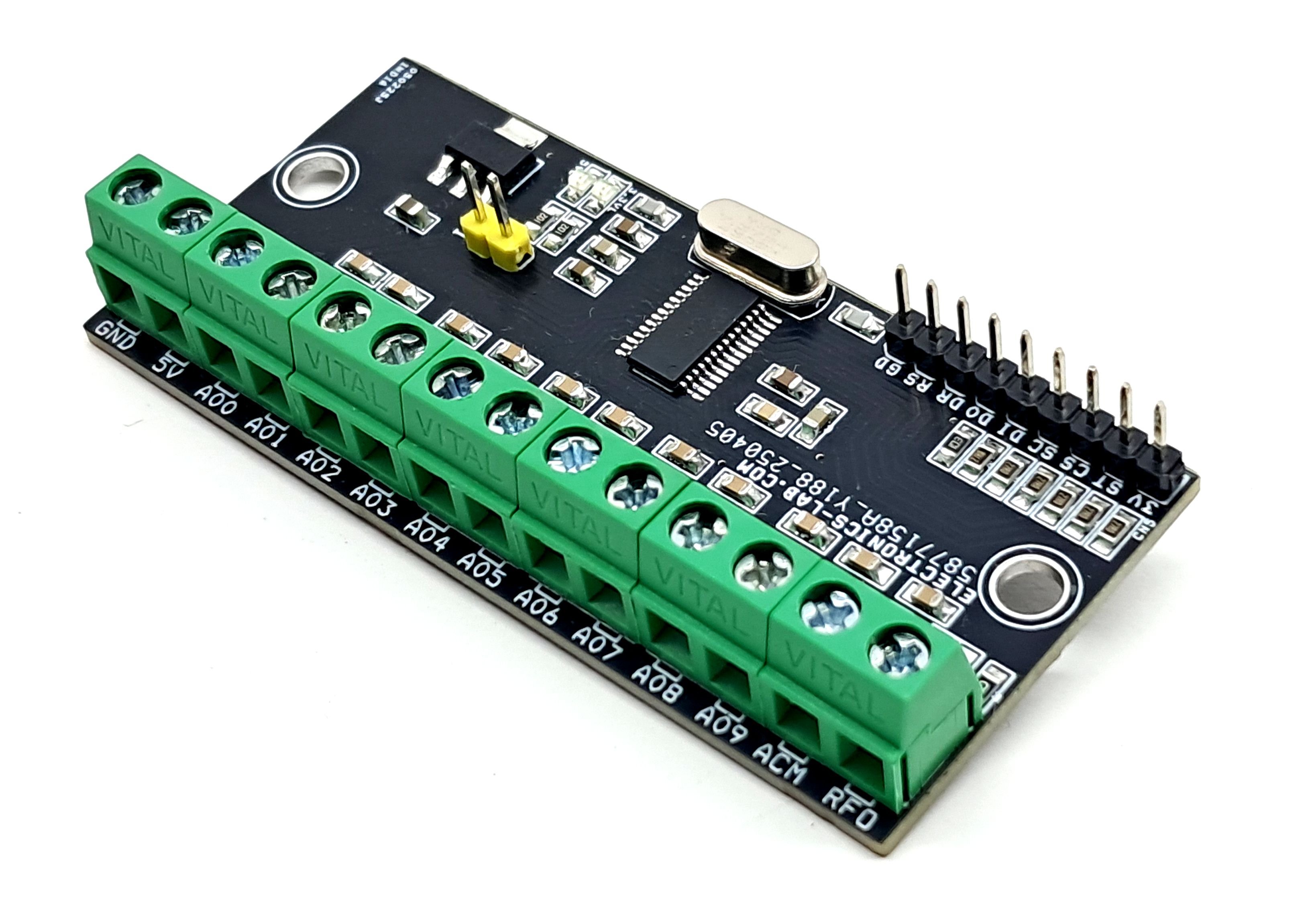
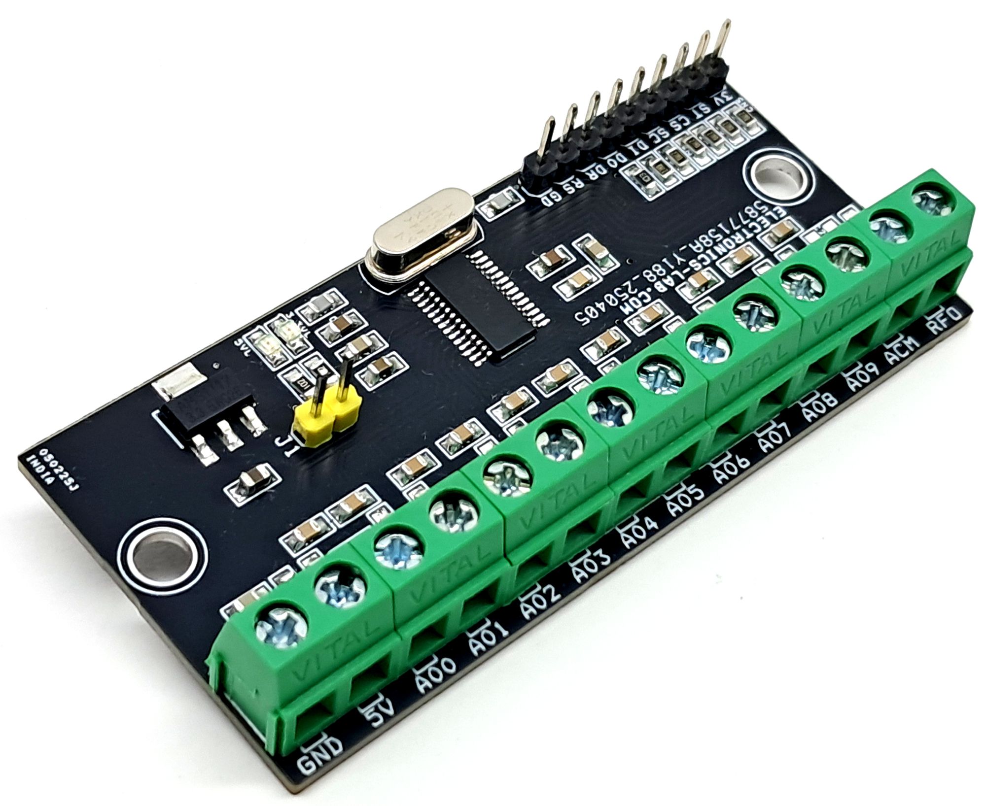
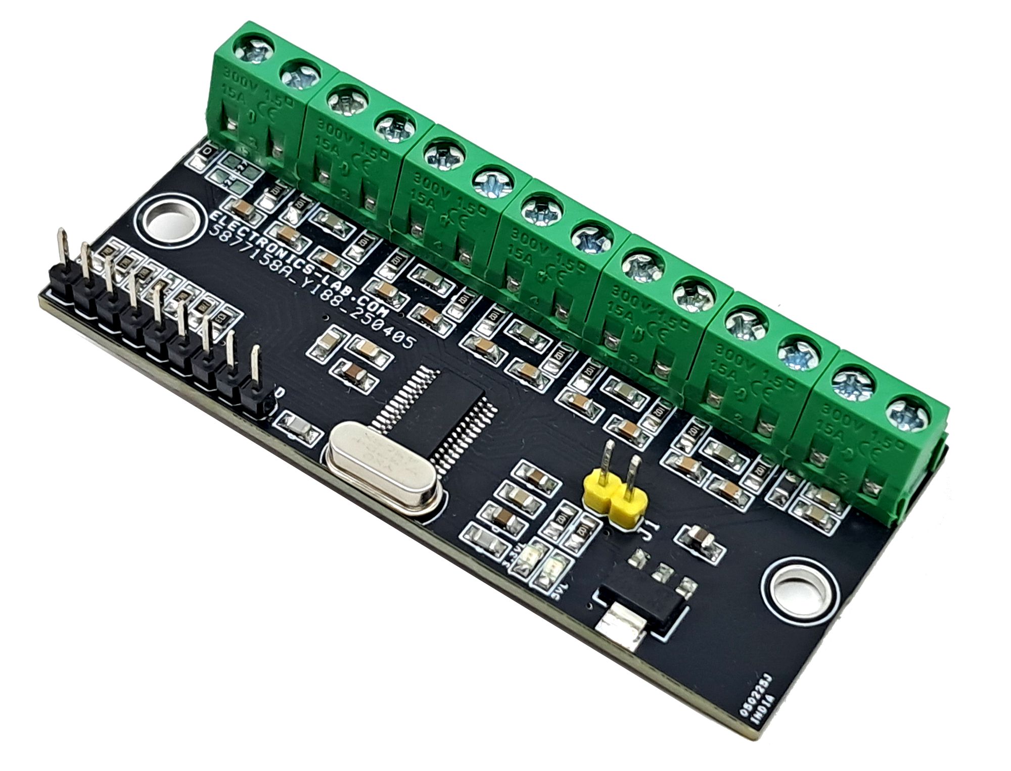
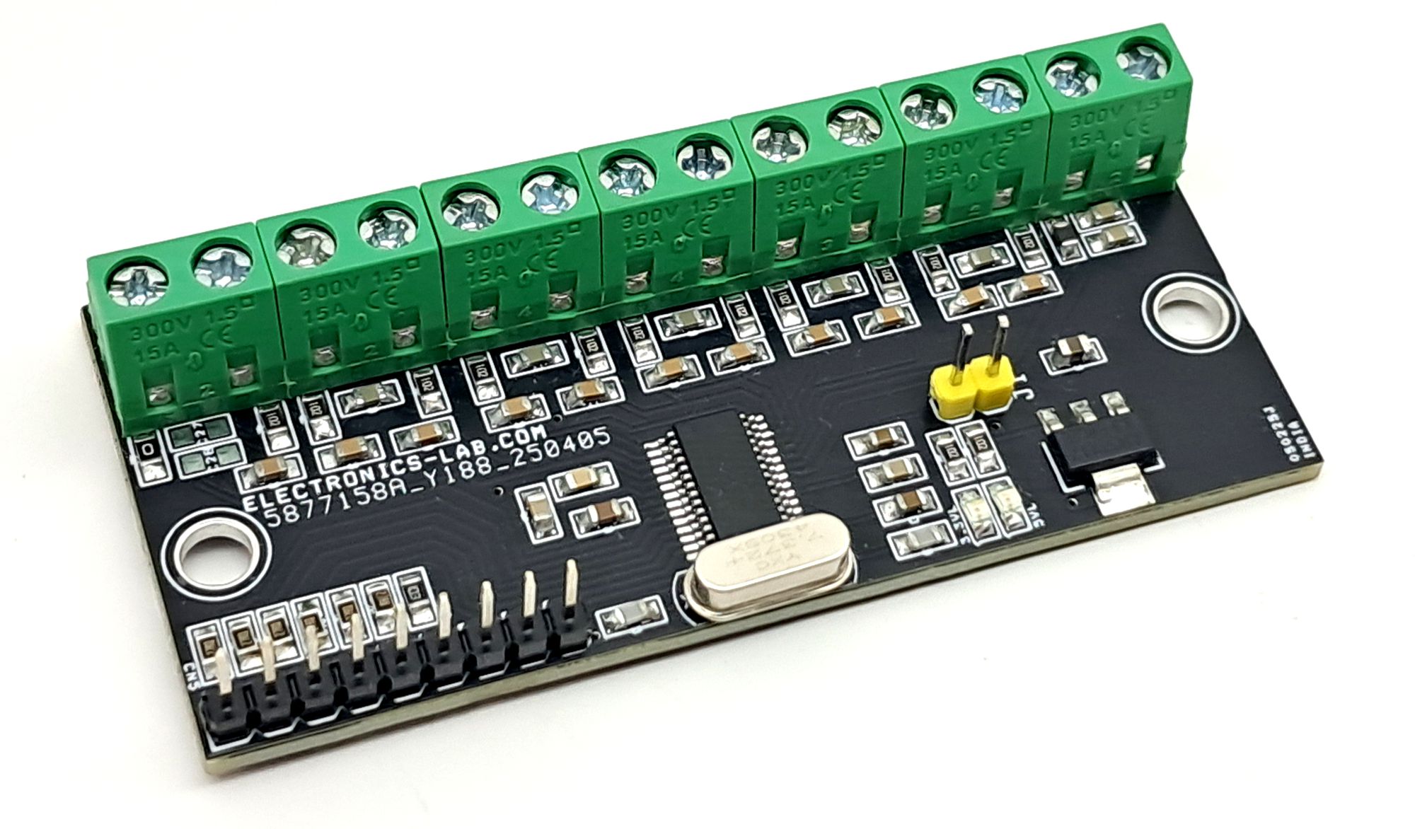
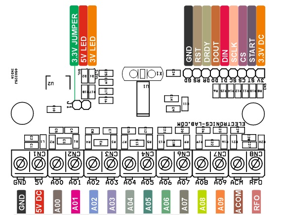
- CN1: Pin 1 = 5V DC Input, Pin 2 = GND
- CN2: Pin 1 = Analog 00 Input, Pin 2 = Analog 01 Input
- CN3: Pin 1 = Analog 02 Input, Pin 2 = Analog 03 Input
- CN4: Pin 1 = Analog 04 Input, Pin 2 = Analog 05 Input
- CN6: Pin 1 = Analog 06 Input, Pin 2 = Analog 07 Input
- CN7: Pin 1 = Analog 08 Input, Pin 2 = Analog 08 Input
- CN8: Pin 1 = ACOM/Analog Common, Pin 2 = Reference Output
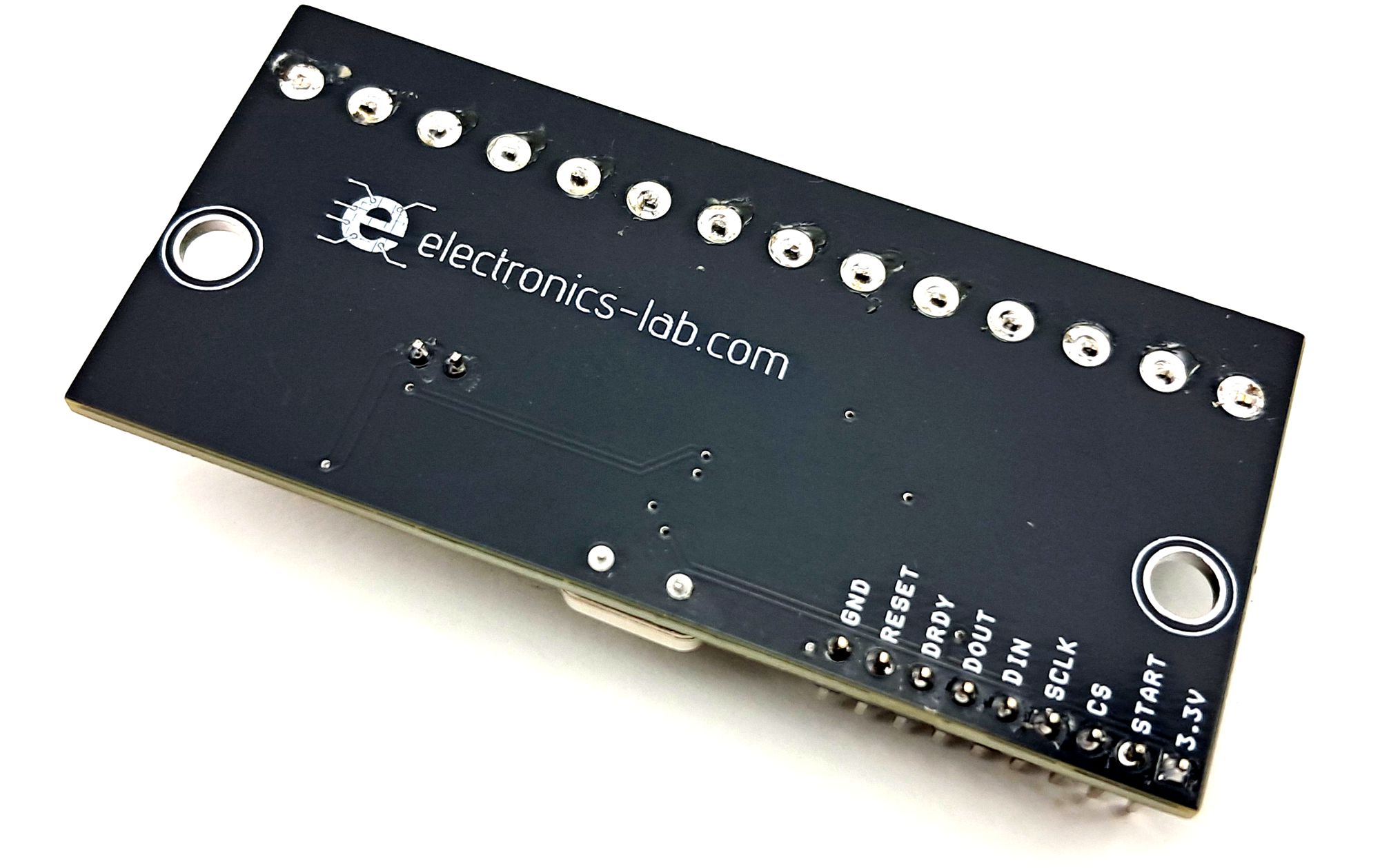
- CN5: Pin 1 = 3.3V DC Input, Pin 2 = Start, Pin 3 = CS, Pin 4 = SCLK, Pin 5 = DIN, Pin 6 = DOUT, Pin 7 = DRDY, Pin 8 = RST, Pin 9 = GND
- D1: 3.3V Power LED
- D2: 5V Power LED
- J1: Jumper for 3.3V Internal or External Selection
Schematic
Parts List
| NO. | QNTY. | REF. | DESC. | MANUFACTURER | SUPPLIER | SUPPLIER PART NO |
|---|---|---|---|---|---|---|
| 1 | 7 | CN1,CN2,CN3,CN4,CN6,CN7,CN8 | 2PIN SCREW TERMINAL PITCH 5.08MM | PHOENIX | DIGIKEY | 277-1247-ND |
| 2 | 1 | CN5 | 9 PIN MALE HEADER PITCH 2.54MM | WURTH | DIGIKEY | 732-5322-ND |
| 3 | 4 | C1,C2,C11,C17 | 100nF/50V CERAMIC SMD SIZE 0805 | YAGEO/MURATA | DIGIKEY | |
| 4 | 5 | C3,C6,C13,C18,C22 | 1.5nF/50V CERAMIC SMD SIZE 0805 | YAGEO/MURATA | DIGIKEY | |
| 5 | 11 | C4,C5,C7,C8,C12,C15,C20,C21,C23,C26,C29 | 150PF/50V CERAMIC SMD SIZE 0805 | YAGEO/MURATA | DIGIKEY | |
| 6 | 1 | C9 | 4.7nF/50C CERAMIC SMD SIZE 0805 | YAGEO/MURATA | DIGIKEY | |
| 7 | 2 | C10,C16 | 10uF/25V CERAMIC SMD SIZE 0805 | YAGEO/MURATA | DIGIKEY | |
| 8 | 2 | C14,C19 | 1uF/25V CERAMIC SMD SIZE 0805 | YAGEO/MURATA | DIGIKEY | |
| 9 | 2 | C24,C25 | 15PF/50V CERAMIC SMD SIZE 0805 | YAGEO/MURATA | DIGIKEY | |
| 10 | 3 | R21,C27,C28 | DNP | |||
| 11 | 2 | D1,D2 | LED RED SMD SIZE 0805 | OSRAM | DIGIKEY | 475-1278-1-ND |
| 12 | 1 | J1 | 2 PIN MALE HEADER PITCH 2.54MM | WURTH | DIGIKEY | 732-5315-ND |
| 13 | 1 | L1 | FERRITE BEAD 150OHM/1A SMD SIZE 0805 | LAIRD | DIGIKEY | 240-2384-1-ND |
| 14 | 12 | R1,R2,R3,R4,R5,R7,R9,R13,R16,R17,R18,R19 | 1K | YAGEO/MURATA | DIGIKEY | |
| 15 | 1 | R6 | 10K | YAGEO/MURATA | DIGIKEY | |
| 16 | 6 | R8,R10,R11,R12,R14,R15 | 47E | YAGEO/MURATA | DIGIKEY | |
| 17 | 1 | R20 | 0E | YAGEO/MURATA | DIGIKEY | |
| 18 | 1 | U1 | ADS1262 TSSOP28 | TI | DIGIKEY | 296-48477-1-ND |
| 19 | 1 | U2 | LM1117-3.3V | TI | DIGIKEY | LM1117MP-3.3/NOPBCT-ND |
| 20 | 1 | X1 | 7.3728MHZ | CTS | DIGIKEY | CTX1035-ND |
| 21 | 1 | J1-SHUNT | SHUNT | SULLINS CONNECT | DIGIKEY | S9001-ND |
Connections
Reference Design
Bridge Measurements
Block Diagram
Pin Connections
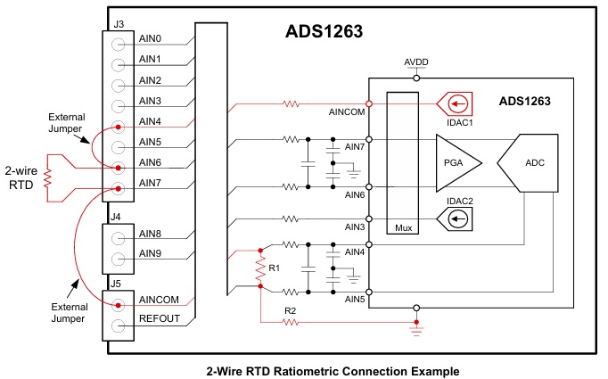
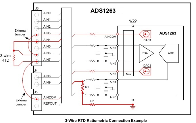
RTD Connections
Gerber View
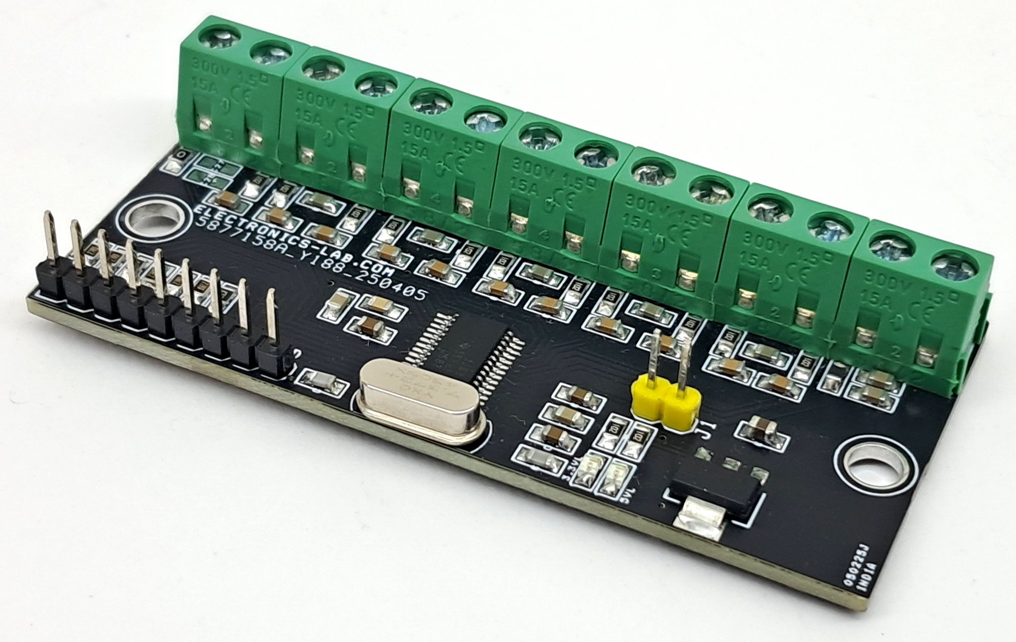
Photos