16-Bit, 500ksps, ±5V SAR ADC with Internal Reference
This module is a 16-bit single channel, pseudo-differential ADC with maximum throughput rates of 500ksps. Both inputs (AIN+ and AIN-) are sampled with a pseudo differential on-chip track-and-hold.
This module is a 16-bit single channel, pseudo-differential ADC with maximum throughput rates of 500ksps. Both inputs (AIN+ and AIN-) are sampled with a pseudo differential on-chip track-and-hold. This ADC includes a precision internal reference.
The project is built using MAX11168 chip which measures a true bipolar voltage of +/-5V (10VPP) and the inputs are protected for up to +/-20mA of overrange current. This ADC is powered from a 4.75V to 5.25V analog supply (VDD) and a separate 2.3V to 5.25V digital supply (OVDD). The MAX11168 requires 500ns to acquire the input sample on an internal track-and-hold and then converts the sampled signal to 16-bits of resolution using an internally clocked converter
Analog Inputs
The MAX11168 ADC consists of a true sampling pseudo differential input stage with high-impedance, capacitive inputs. The internal T/H circuitry features a small-signal bandwidth of about 6MHz to provide 16-bit accurate sampling in 500ns. This allows for accurate sampling of a number of scanned channels through an external multiplexer.
The MAX11168 on the AIN+ input, accurately converts input signals in the interval from AIN- to (±5V + AIN-). AIN+ has a max input interval from -5.1V to +5.1V. AIN- has a max input interval from -0.1V to +0.1V. The MAX11168 performs a true differential sampling on inputs between AIN+ and AIN- with good common-mode rejection (see the Typical Operating Circuit). This allows for improved sampling of remote transducer inputs. Many traditional ADCs with single supplies that measure bipolar input signals use resistive divider networks directly on the analog inputs. These networks increase the complexity of the input signal conditioning. However, the MAX11168 includes a patented input switch architecture that allows direct sampling of high-impedance sources. This architecture requires a minimum sample rate of 10Hz to maintain accurate conversions over the designed temperature and supply ranges.
Features
- 5V Analog Supply (VD/VDD)
- 3V to 5V Digital Supply (VC/OVDD)
- 6mW Power Consumption at 500ksps
- 10µA in Shutdown Mode
- High DC/AC Accuracy Improves Measurement Quality
- 16-Bit Resolution with No Missing Codes
- 500ksps Throughput Rates Without Pipeline Delay/Latency
- 3dB SNR and -101dB THD at 10kHz
- 5 LSBRMS Input-Referred Noise
- ±0.2 LSB DNL (typ) and ±0.75 LSB INL (typ)
- Highly Integrated ADC Saves Cost and Space
- ±7ppm/°C Internal Reference
- Internal Reference Buffer
- ±5V Bipolar Analog Input Range
- PCB Dimensions 18.89x 15.88 mm
Overvoltage Input Clamp
The MAX11168 includes an input clamping circuit that activates when the input voltage at AIN+ is above (VDD + 300mV) or below -(VDD + 300mV). The clamp circuit remains high impedance while the input signal is within the range of Q (VDD + 100mV) and draws little to no current. However, when the input signal exceeds this range, the clamps begin to turn on. Consequently, to obtain the highest accuracy, ensure that the input voltage does not exceed the range of Q (VDD + 100mV). To make use of the input clamps, connect a resistor (RS) between the AIN+ input and the voltage source to limit the voltage at the analog input and to ensure the fault current into the devices does not exceed Q20mA.
Reference
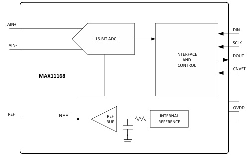
The MAX11168 includes a precision internal reference source as well as an internal reference buffer circuit to drive the converter.
The MAX11168 is a 16-bit, 500ksps, SAR ADC offering excellent AC and DC performance with true bipolar input range, internal reference, and small size. The MAX11168 measures a ±5V (10VP-P) input range while operating from a single 5V supply. A patented charge-pump architecture allows direct sampling of high-impedance sources. The MAX11168 integrates a low drift reference with internal buffer, saving the cost and space of an external reference. This ADC achieves 92.3dB SNR and -101dB THD. The MAX11168 guarantees 16-bit no-missing codes and ±0.75 LSB INL (typ). The MAX11168 communicates using an SPI-compatible serial interface at 2.5V, 3V, 3.3V, or 5V logic. The serial interface can be used to daisy-chain multiple ADCs for multichannel applications and provides a busy indicator option for simplified system synchronization and timing.
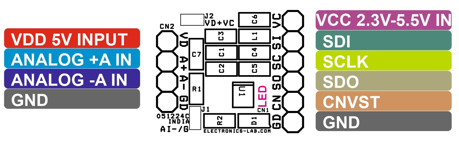
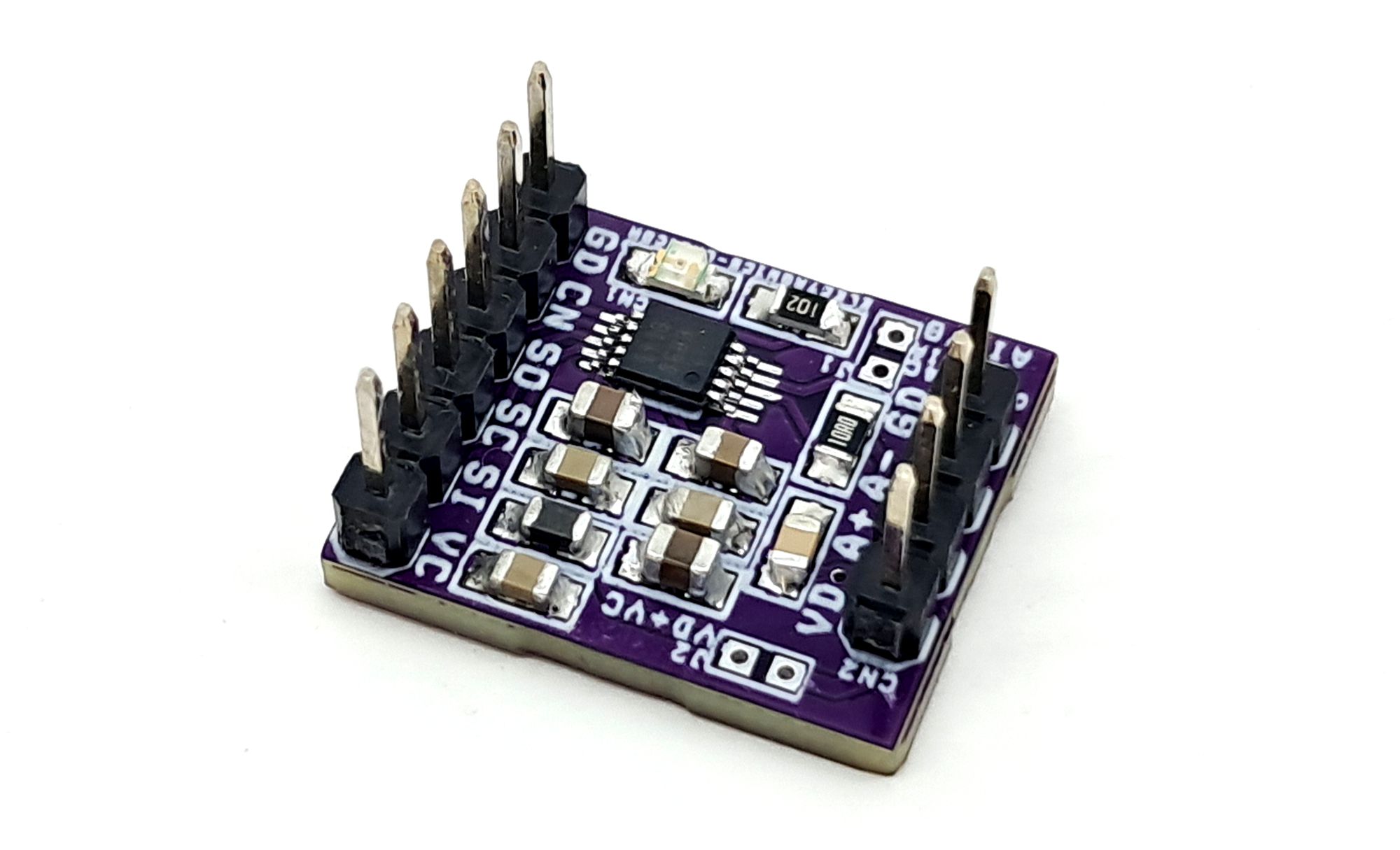
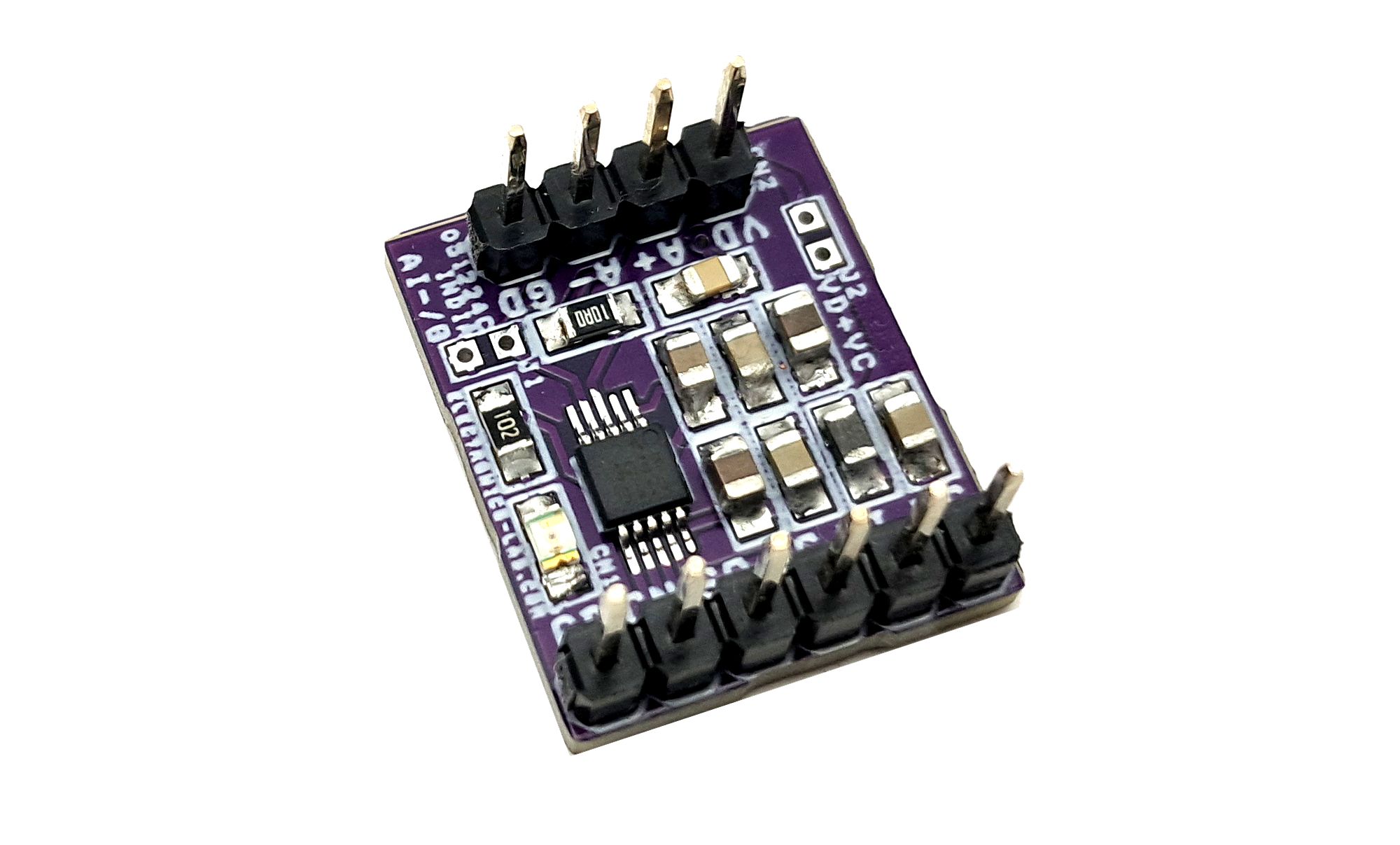
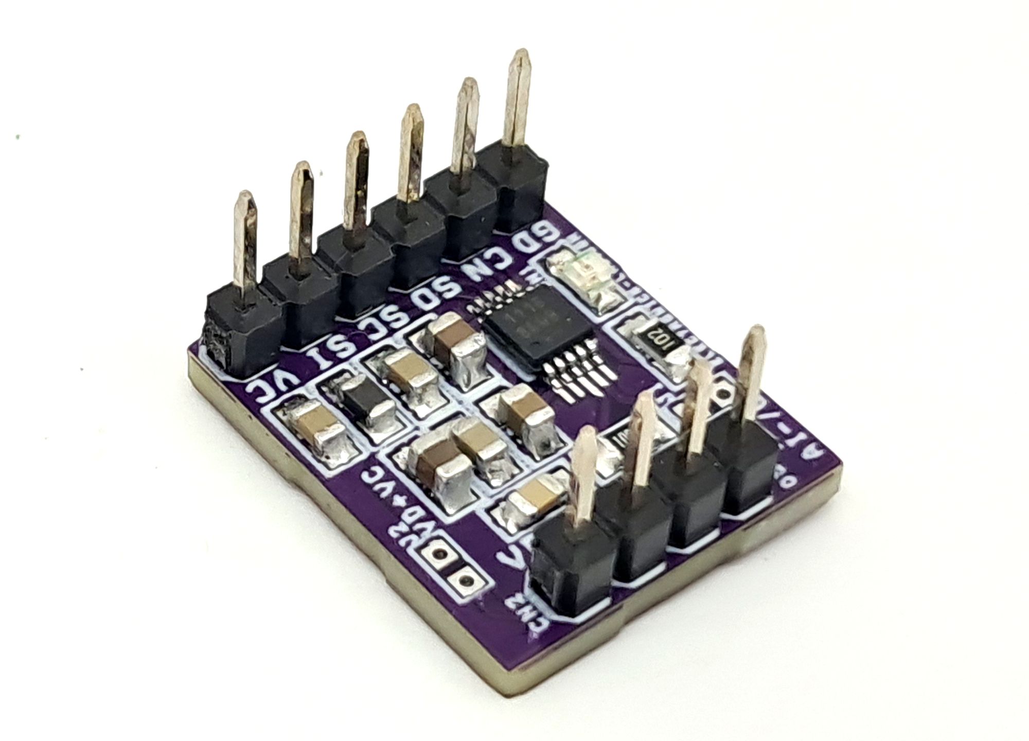
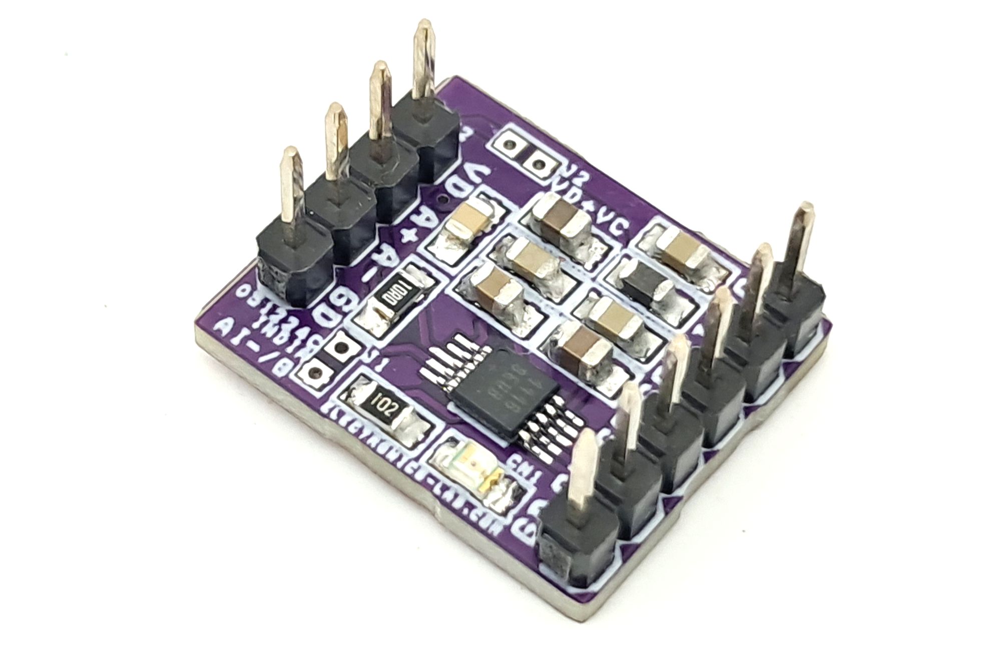
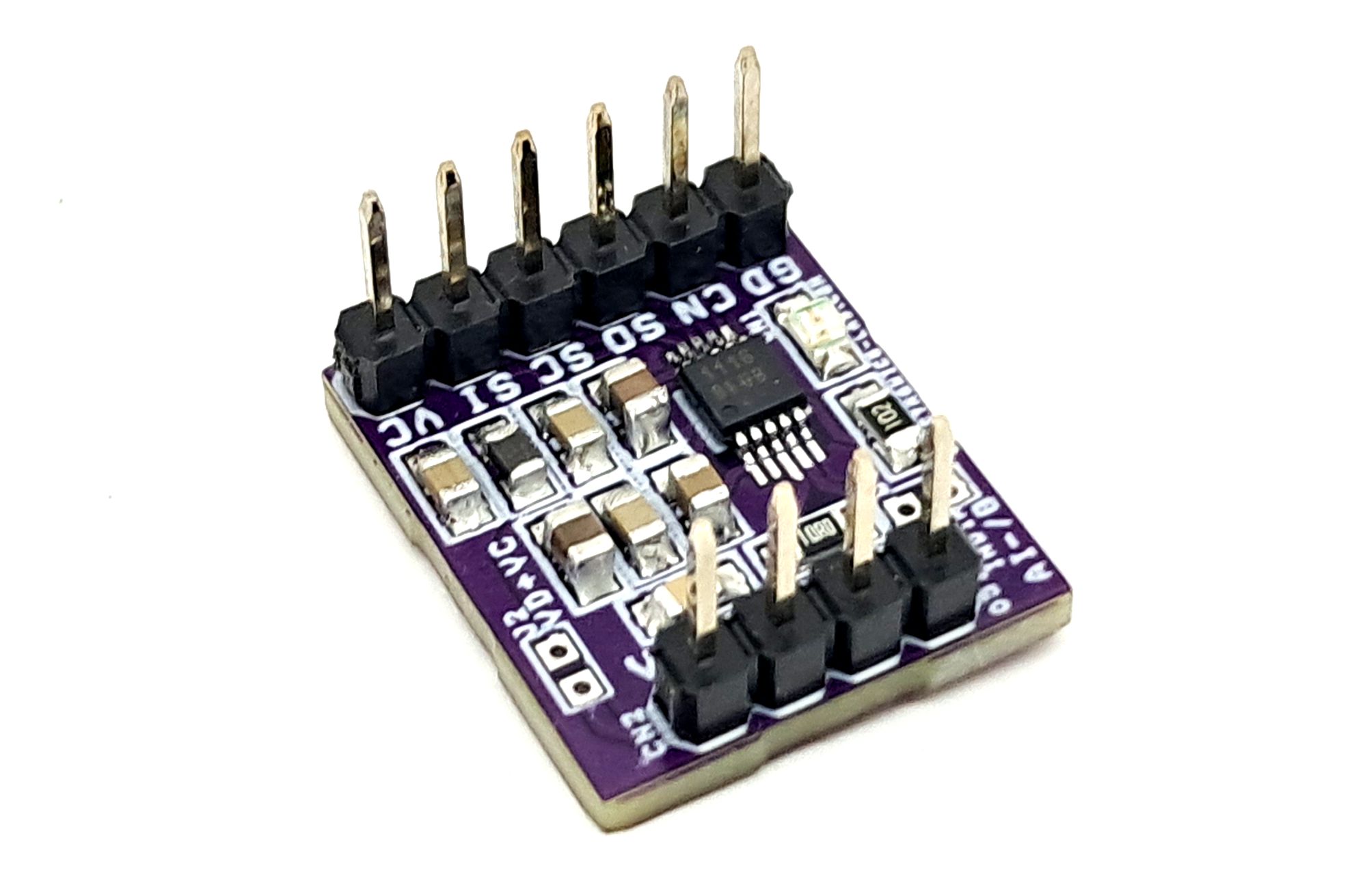
Connections
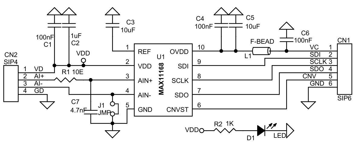
- CN1: Pin 1 = VCC, Pin 2 = SDI, Pin 3 = SCLK, Pin 4 = SDO, Pin 5 = CNVST, Pin 6 = GND
- CN2: Pin 1 = VDD, Pin 2 = Input +A, Pin 3 = Input -A, Pin 4 = GND
- D1: Power LED
Schematic
Parts List
| NO. | QNTY. | REF. | DESC | MANUFACTURER | SUPPLIER | SUPPLIER PART NO |
|---|---|---|---|---|---|---|
| 1 | 1 | CN1 | 6 PIN MALE HEADER PITCH 2.54MM | WURTH | 732-5319-ND | |
| 2 | 1 | CN2 | 4 PIN MALE HEADER PITCH 2.54MM | WURTH | 732-5317-ND | |
| 3 | 3 | C1,C4,C6 | 100nF/50V CERAMIC SMD SIZE 0805 | YAGEO/MURATA | ||
| 4 | 1 | C2 | 1uF/16V CERAMIC SMD SIZE 0805 | YAGEO/MURATA | ||
| 5 | 2 | C3,C5 | 10uF/16V CERAMIC SMD SIZE 0805 | YAGEO/MURATA | ||
| 6 | 1 | C7 | 4.7nF/50V CERAMIC SMD SIZE 0805 | YAGEO/MURATA | ||
| 7 | 1 | D1 | LED RED SMD SIZE 0805 | OSRAM | 475-1278-1-ND | |
| 8 | 1 | J1 | JMP-SOLDER | |||
| 9 | 1 | L1 | F-BEAD 600OHM SMD SIZE 0805 | LAIRD | 240-2390-1-ND | |
| 10 | 1 | R1 | 10E 5% SMD SIZE 0805 | YAGEO/MURATA | ||
| 11 | 1 | R2 | 1K 5% SMD SIZE 0805 | YAGEO/MURATA | ||
| 12 | 1 | U1 | MAX11168 | ANALOG DEVICE | MAX11168EUB+-ND |
Connections
Block Diagram
Gerber View
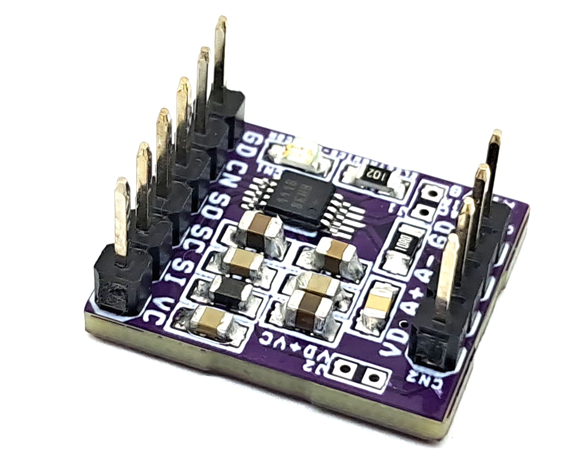
Photos
Where to buy