Digitally Controlled Audio Processor using TDA7440
TDA7440 Audio: I2C-based Hi-Fi volume, tone, and balance control with selectable input gain.
This Audio Processor designed using TDA7440 chip from ST. The chip is a volume tone (bass and treble) balance (Left/Right) processor for quality audio applications in Hi-Fi systems. A selectable input gain is provided. Control of all the functions is accomplished by serial bus I2C. The AC signal setting can be altered by resistor networks and switches combined with operational amplifiers.
Features
- Supply 9V DC (Range 6V to 10V)
- All functions Programmable Via I2C Serial Bus
- 4 Channel Stereo Inputs, Multiplexer, I2C Selectable
- Treble and Bass Control 2.0dB Steps
- One Channel Stereo Output
- Two Speaker Attenuators, Two Independ Speaker Control In 1.0dB Steps for Balance
- Volume Control In 1.0dB Steps
- Screw Terminals for Audio Inputs and Outputs
- Header Connector for I2C Digital Interface
- Header Connector for Power Input
- On Board Power LED
- 4 x 4MM PCB Mounting Holes
- PCB Dimensions 82.55 x 44.93 mm
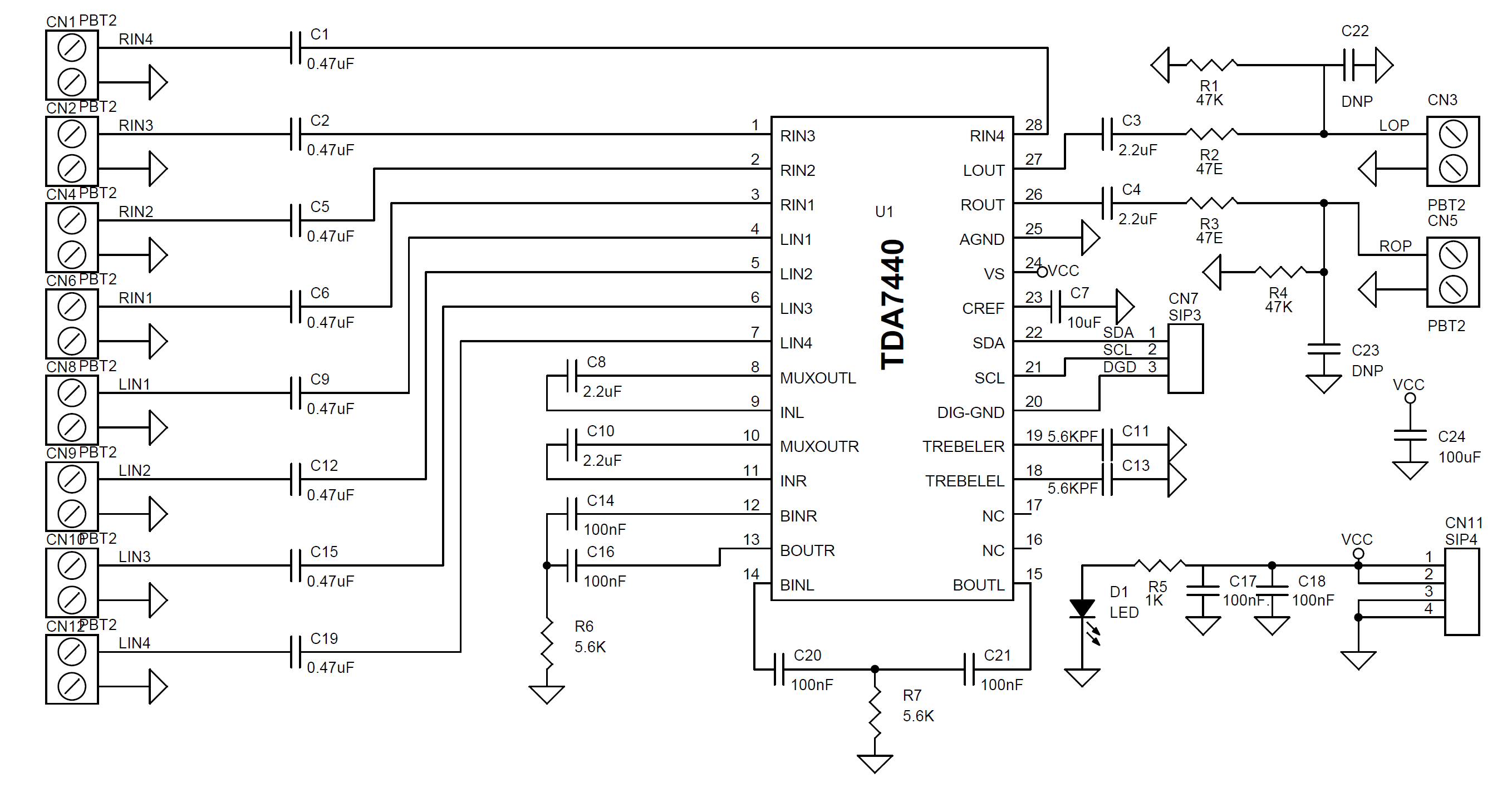
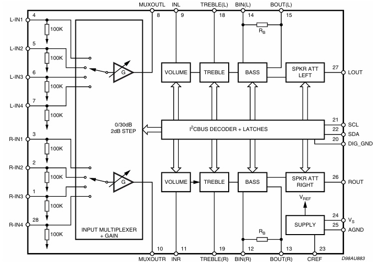
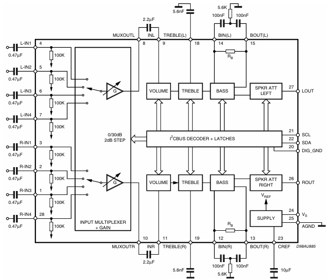
TDA7440
The first and the last stages are volume control blocks. The control range is 0 to -47dB (mute) for the first one, 0 to -79dB (mute) for the last one. Both of them have 1dB step resolution. The very high resolution allows the implementation of systems free from any noisy acoustical effect. The TDA7440D audio processor provides 3 bands tones control.
Treble Stage
The treble stage is a high pass filter whose time constant is fixed by an internal resistor (25KΩ typical) and an external capacitor connected between treble pins and ground.
I2C BUS INTERFACE
Data transmission from microprocessor to the TDA7440D and vice versa takes place through the 2 wires I2C BUS interface, consisting of the two lines SDA and SCL (pull-up resistors to positive supply voltage must be connected).
Data Validity
As shown in fig. 11, the data on the SDA line must be stable during the high period of the clock. The HIGH and LOW state of the data line can only change when the clock signal on the SCL line is LOW.
Start and Stop Conditions
As shown in schematic a start condition is a HIGH to LOW transition of the SDA line while SCL is HIGH. The stop condition is a LOW to HIGH transition of the SDA line while SCL is HIGH.
Byte Format
Every byte transferred on the SDA line must contain 8 bits. Each byte must be followed by an acknowledge bit. The MSB is transferred first.
Acknowledge
The master (µP) puts a restive HIGH level on the SDA line during the acknowledge clock pulse (see fig. 13). The peripheral (audio processor) that acknowledges has to pull-down (LOW) the SDA line during this clock pulse. The audio processor which has been addressed has to generate an acknowledge after the reception of each byte, otherwise the SDA line remains at the HIGH level during the ninth clock pulse time. In this case the master transmitter can generate the STOP information in order to abort the transfer.
Transmission without Acknowledge
Avoiding to detect the acknowledge of the audio processor, the µP can use a simpler transmission: simply it waits one clock without checking the slave acknowledging, and sends the new data. This approach of course is less protected from mis working.
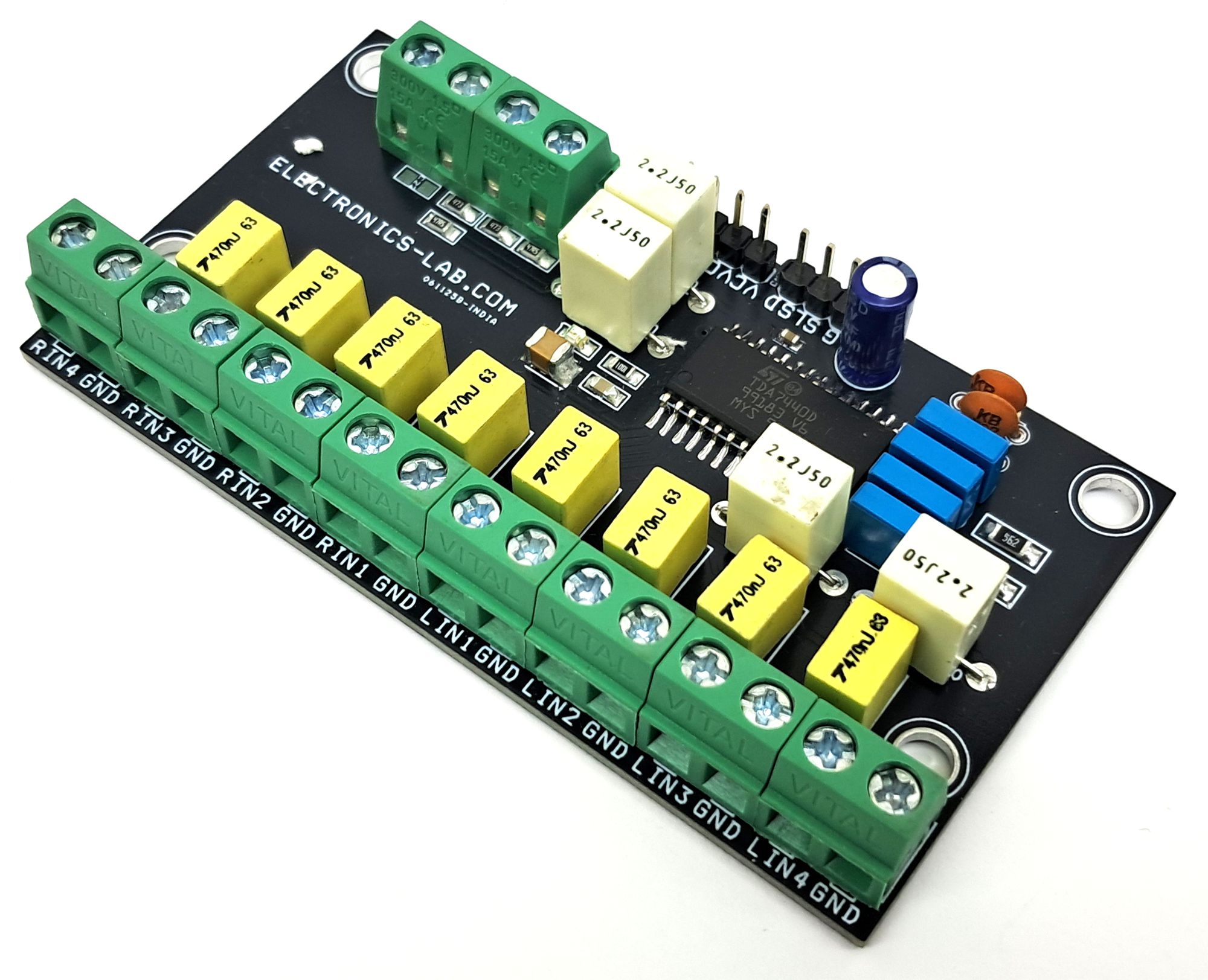
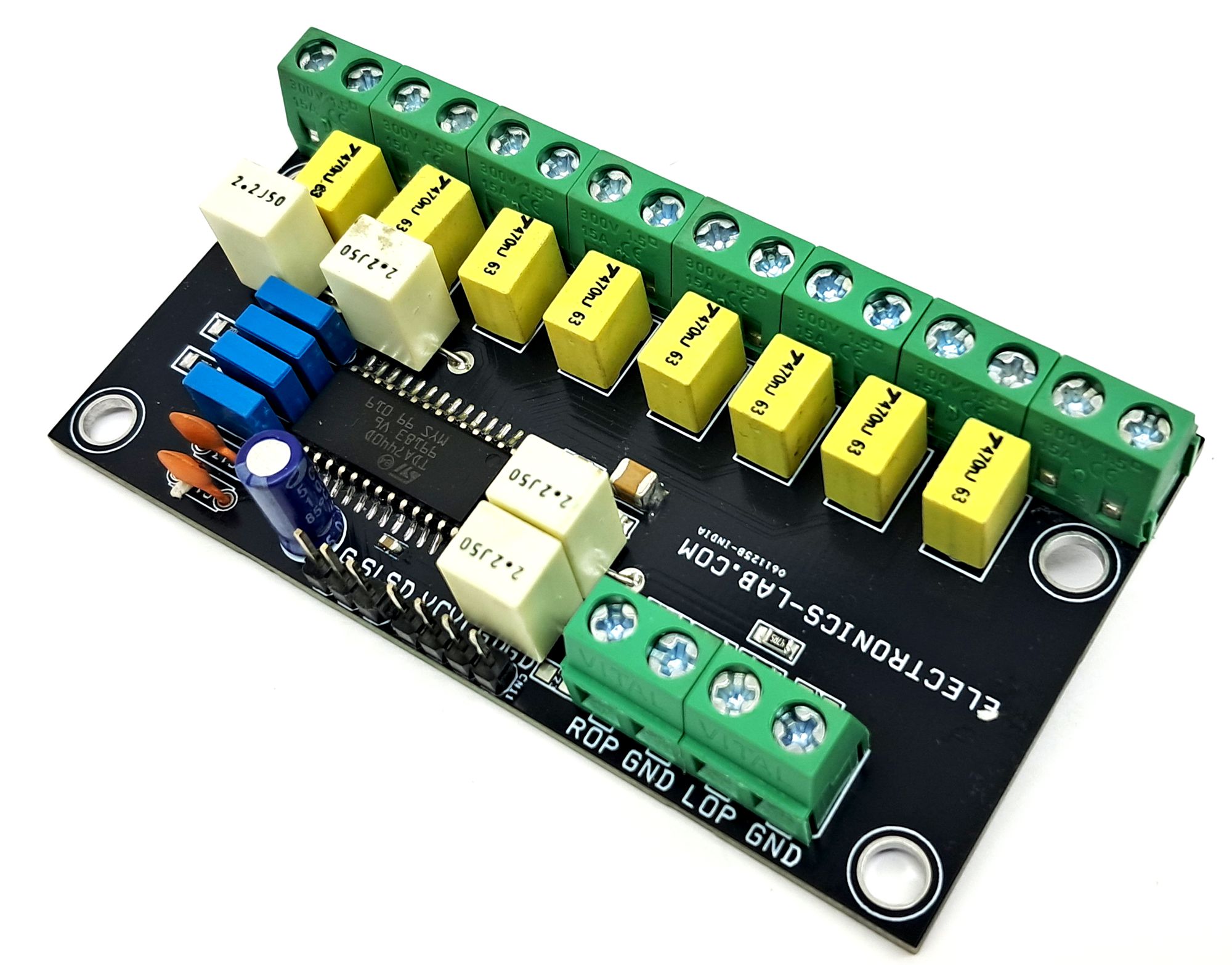
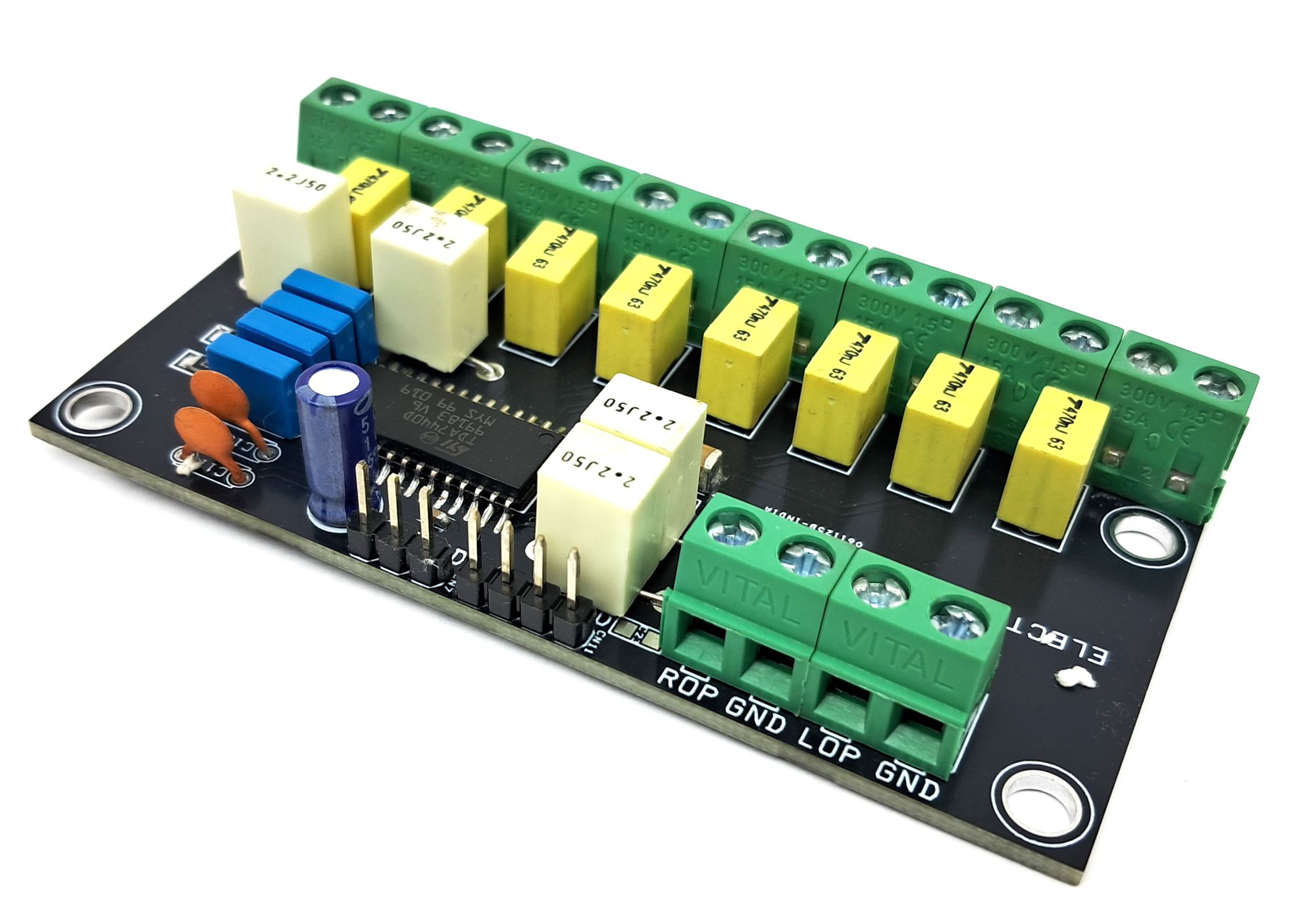
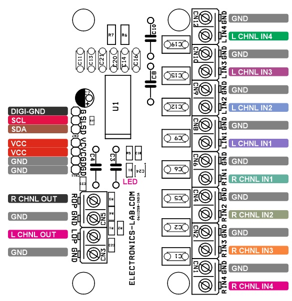
Connections
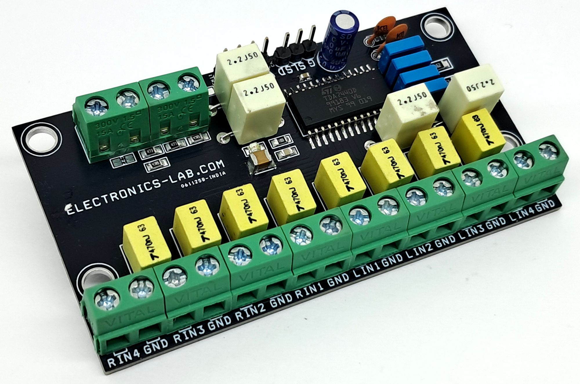
- CN1: Pin 1 = Right Channel Audio In4, Pin 2 = GND
- CN2: Pin 1 = Right Channel Audio In3, Pin 2 = GND
- CN4: Pin 1 = Right Channel Audio In2, Pin 2 = GND
- CN6: Pin 1 = Right Channel Audio In1, Pin 2 = GND
- CN8: Pin 1 = Left Channel Audio In1, Pin 2 = GND
- CN9: Pin 1 = Left Channel Audio In2, Pin 2 = GND
- CN10: Pin 1 = Left Channel Audio In3, Pin 2 = GND
- CN12: Pin 1 = Left Channel Audio In4, Pin 2 = GND
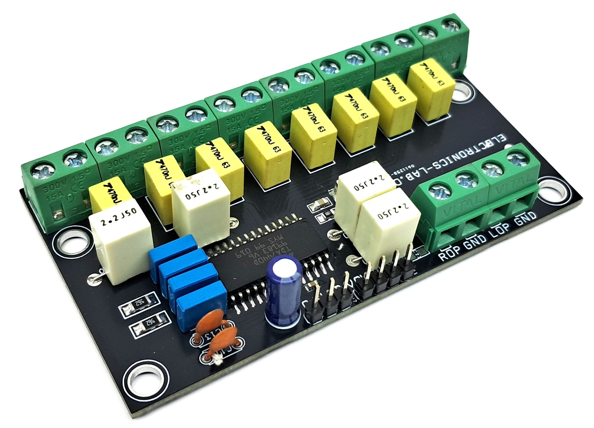
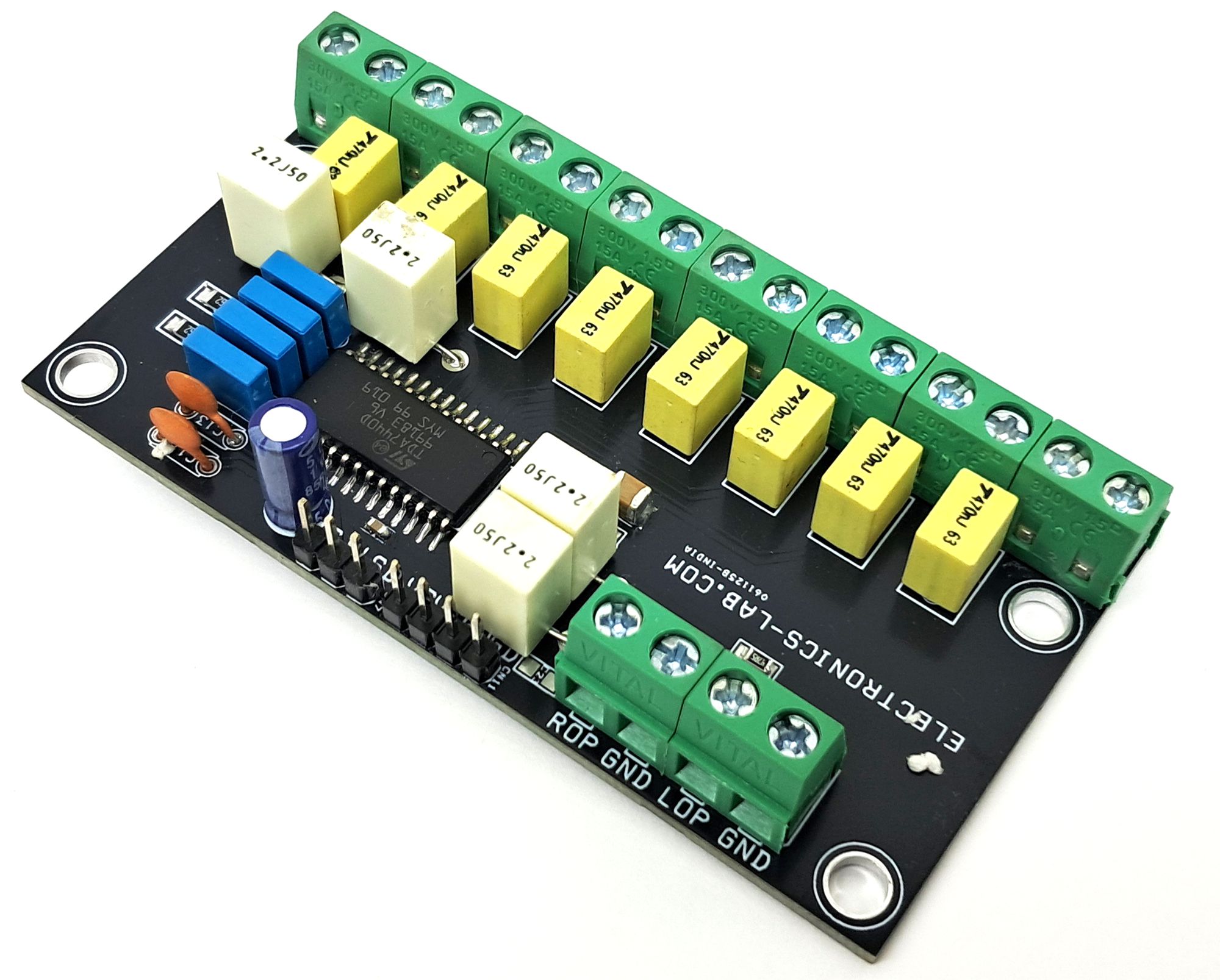
- CN3: Pin 1 Left Channel Audio Output, Pin 2 = GND
- CN5: Pin 1 Right Channel Audio Output, Pin 2 = GND
- CN7: Pin 1 SDA Digital Pin, Pin 2 = SCL Digital Pin, Pin 3 = Digital GND
- CN11: Pin 1,2 = VCC, Pin 3,4 = GND
- D1: Power LED
Schematic
Parts List
| NO. | QNTY. | REF. | DESC. | MANUFACTURER | SUPPLIER | SUPPLIER PART NO |
|---|---|---|---|---|---|---|
| 1 | 10 | CN1,CN2,CN3,CN4,CN5,CN6,CN8,CN9,CN10,CN12 | 2 PIN SCREW TERMINAL PITCH 5.08MM | PHOENIX | DIGIKEY | 277-1247-ND |
| 2 | 1 | CN7 | 3 PIN MALE HEADER PITCH 2.54MM | WURTH | DIGIKEY | 732-5316-ND |
| 3 | 1 | CN11 | 4 PIN MALE HEADER PITCH 2.54MM | WURTH | DIGIKEY | 732-5317-ND |
| 4 | 8 | C1,C2,C5,C6,C9,C12,C15,C19 | 0.47uF/63V FILM CAPACITOR 5X7MM | DIGIKEY | ||
| 5 | 1 | C7 | 10uF/50V ELECTROLYTIC 5X11MM | DIGIKEY | ||
| 6 | 4 | C3,C4,C8,C10 | 2.2uF/50V 7X11MM THT | DIGIKEY | ||
| 7 | 2 | C11,C13 | 5.6KPF/50V CERAMIC DISC TYPE | DIGIKEY | ||
| 8 | 4 | C14,C16,C20,C21 | 100nF/63V FILM CAPACITOR 2.5X7MM THT | DIGIKEY | ||
| 9 | 1 | C17 | 100nF/16V CERAMIC SMD SIZE 0603 | YAGEO/MURATA | DIGIKEY | |
| 10 | 2 | C22,C23 | DNP | |||
| 11 | 1 | C24 | 47uF OR 100uF/16V CERAMIC SMD SIZE 1210 | YAGEO/MURATA | DIGIKEY | |
| 12 | 1 | D1 | LED RED SMD SIZE 0805 | OSRAM | DIGIKEY | 475-1278-1-ND |
| 13 | 2 | R1,R4 | 47K 5% SMD SIZE 0805 | YAGEO/MURATA | DIGIKEY | |
| 14 | 2 | R2,R3 | 47E 5% SMD SIZE 0805 | YAGEO/MURATA | DIGIKEY | |
| 15 | 1 | R5 | 1K 5% SMD SIZE 0805 | YAGEO/MURATA | DIGIKEY | |
| 16 | 2 | R6,R7 | 5.6K 5% SMD SIZE 1206 | YAGEO/MURATA | DIGIKEY | |
| 17 | 1 | U1 | TDA7440 SOIC28 | ST | DIGIKEY | 497-8883-1-ND |
| 18 | 1 | C18 | 100nF/16V CERAMIC SMD SIZE 0805 | YAGEO/MURATA | DIGIKEY |
Connections
Block Diagram
Application Diagram
Gerber View
Photos