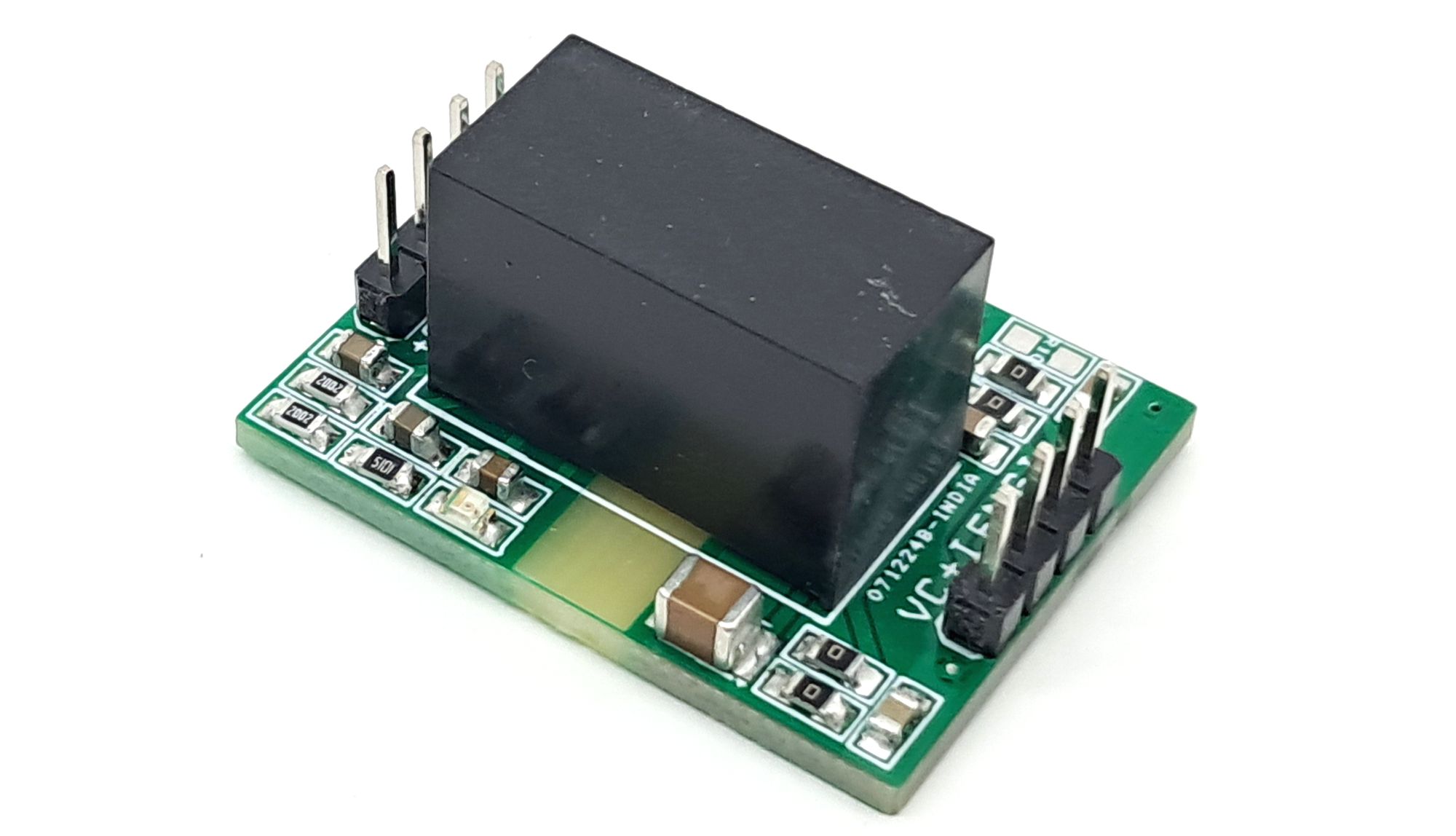
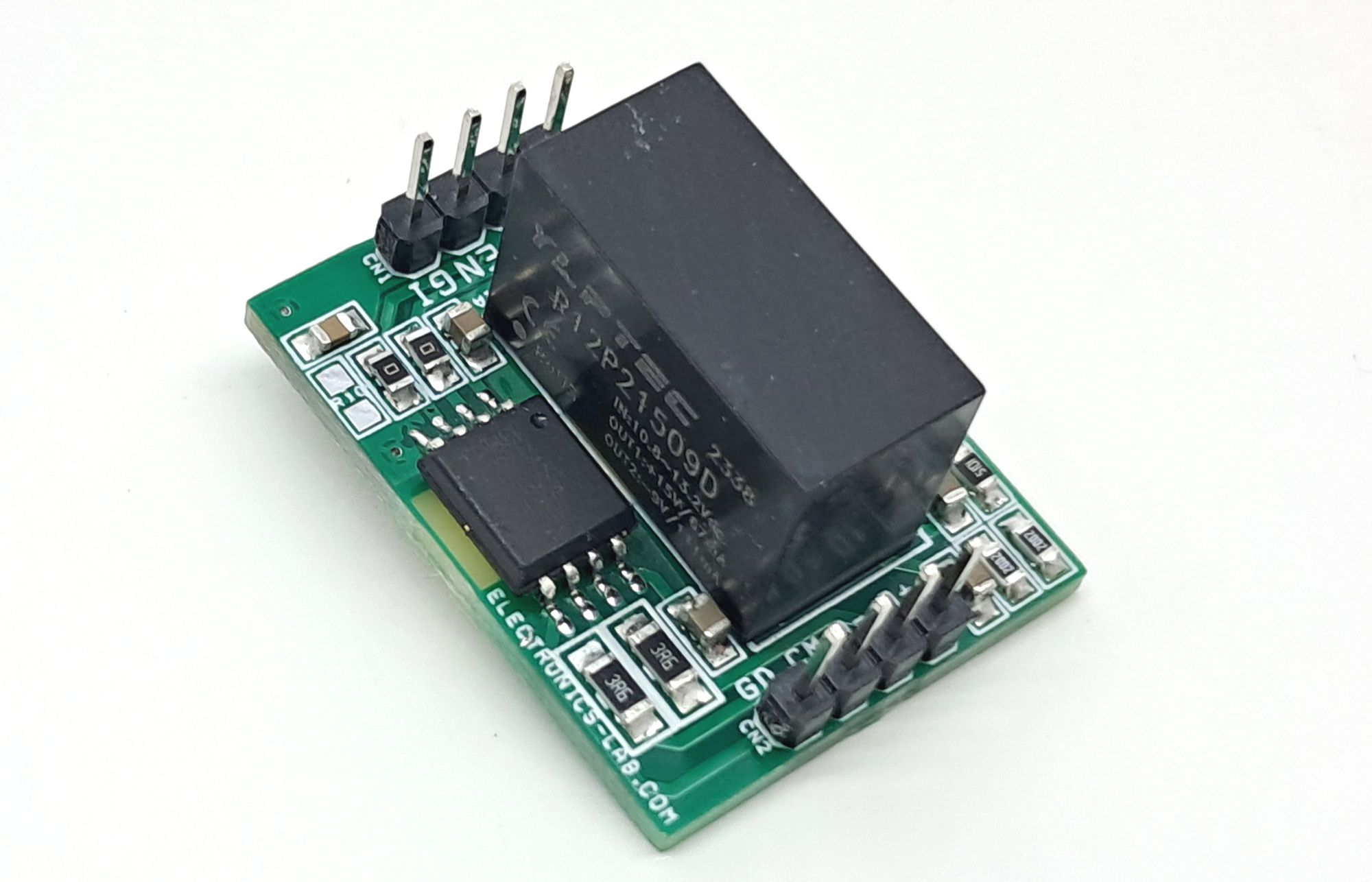
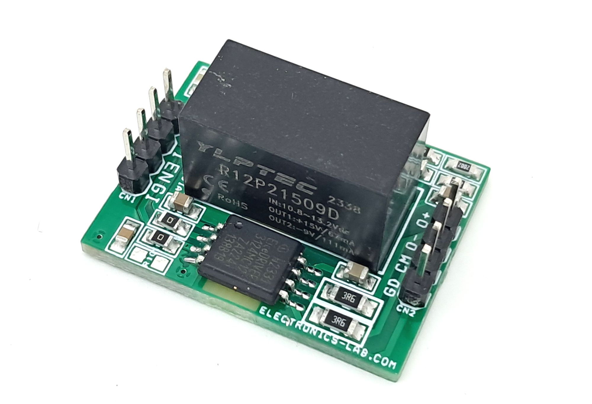
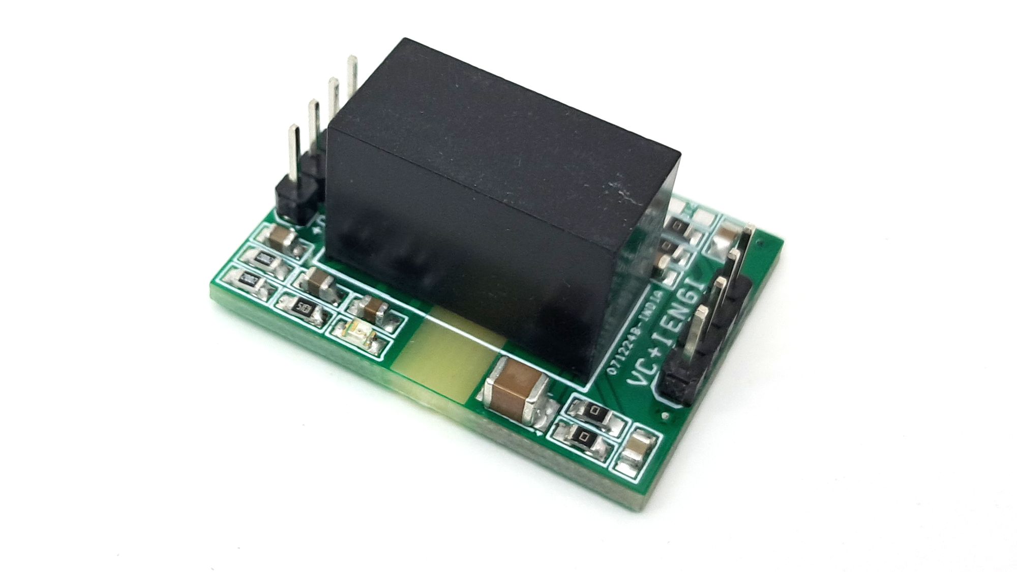
High Current Isolated Gate Driver for IGBTs
The project design features a galvanically isolated single-channel gate driver IC with a dedicated isolated DC-DC gate drive power supply providing bipolar output of +15V/-9V. This compact module is designed to control IGBTs in inverters, offering high gate driver currents up to 14A for applications like half-bridge, full-bridge, and single IGBT. The driver operates in two modes, non-inverting and inverting, with a minimum input pulse width to filter glitches. The output driver section uses MOSFETs for rail-to-rail output to control gate voltage during on-state and short circuits efficiently. This setup is suitable for use with various IGBT voltages and features optimizations for high-frequency operations.
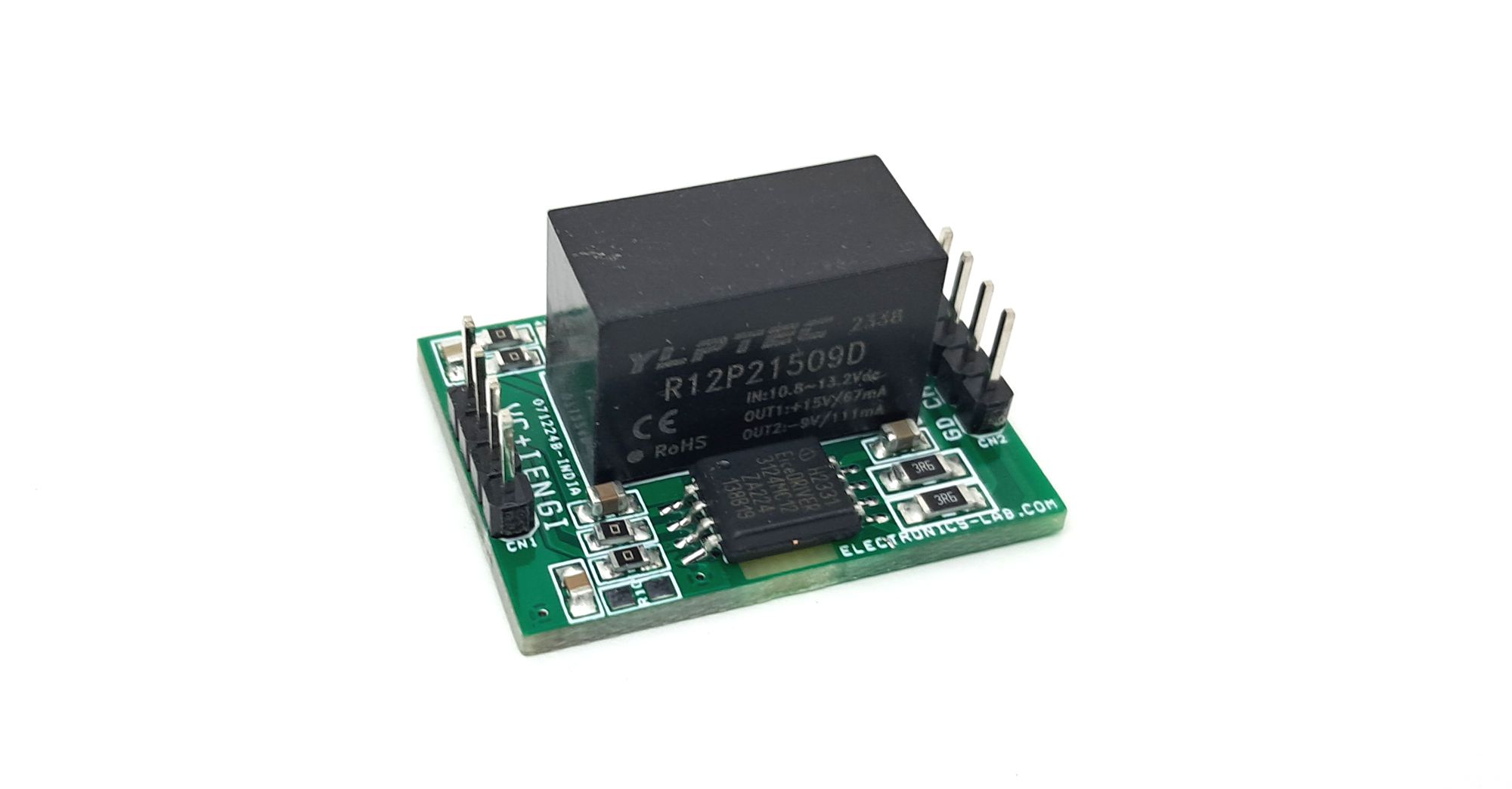
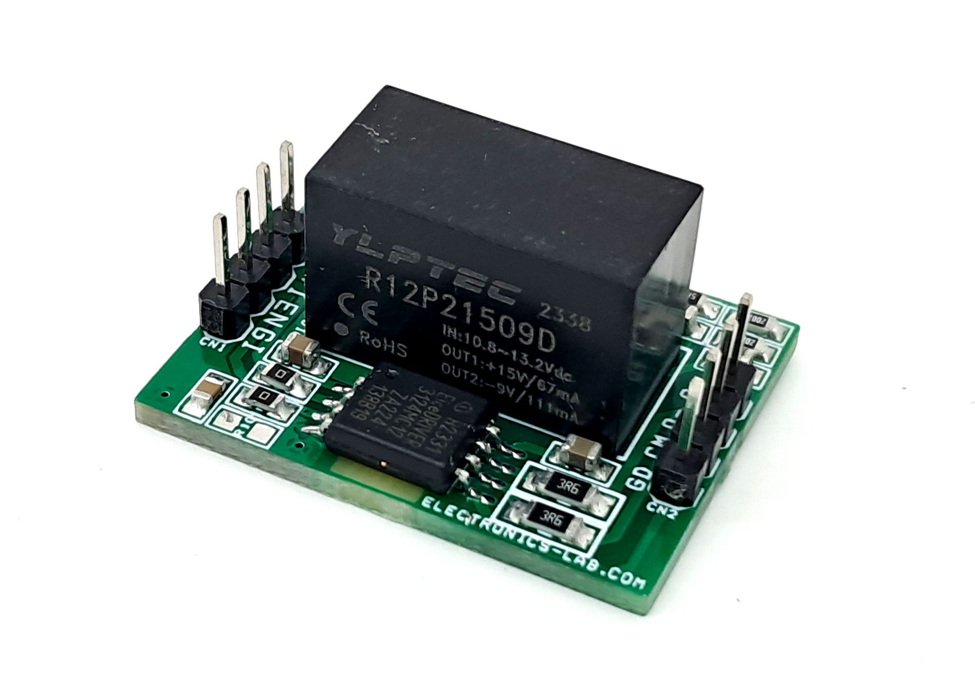
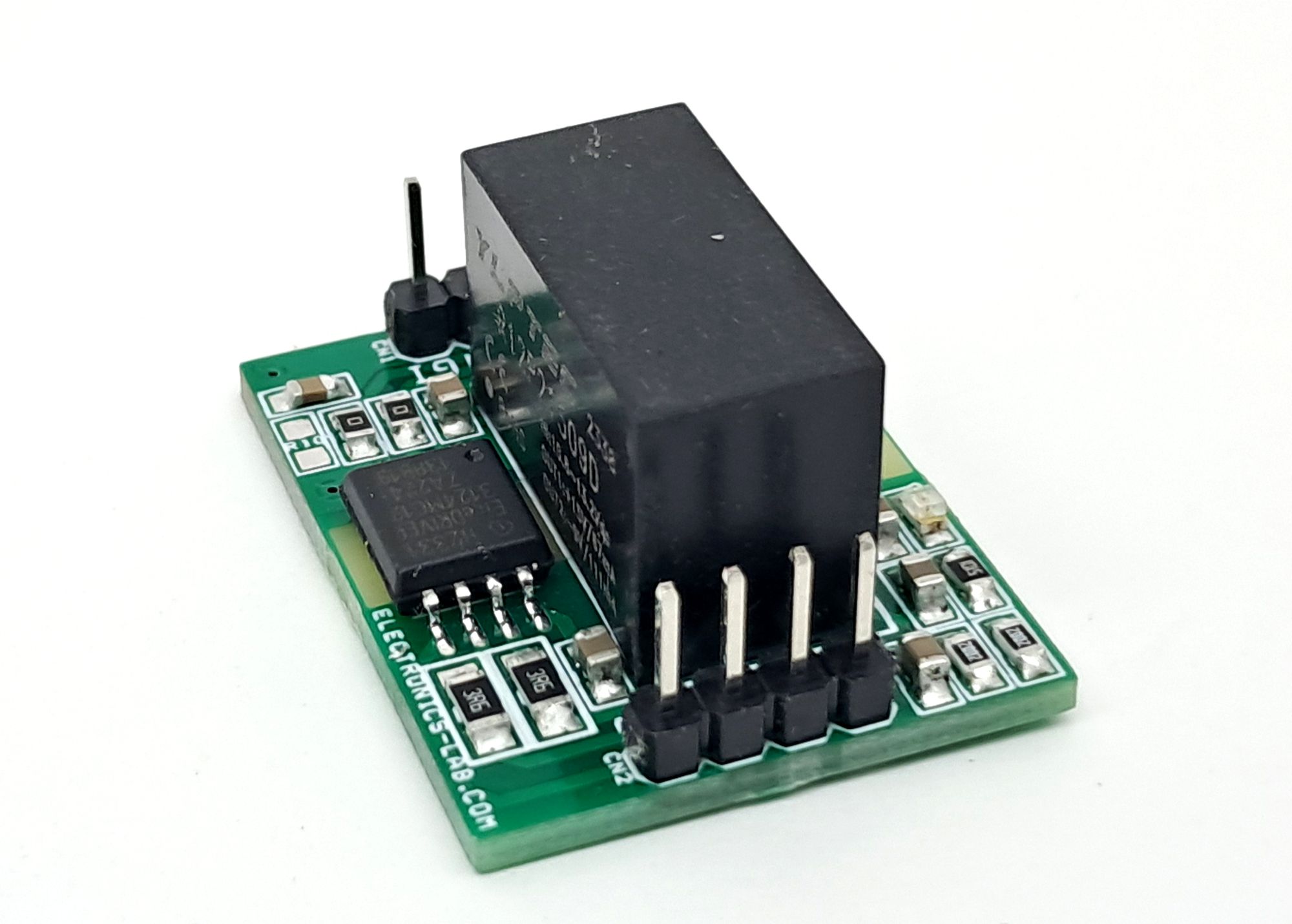
This project design consists of galvanically isolated single channel gate driver IC and dedicated isolated DC-DC gate drive power supply with bipolar output +15V/-9V. This compact module can control IGBTs in inverters. The isolated high current IGBT gate driver module is a simple solution for power drivers, consisting of a gate driver chip 1ED3124MC12H and an isolated 2W DC-DC converter (R12P21509D). This module is optimized for high-frequency operations and can provide high gate driver currents up to 14A, making it suitable for applications such as half-bridge, full-bridge, and single IGBT.
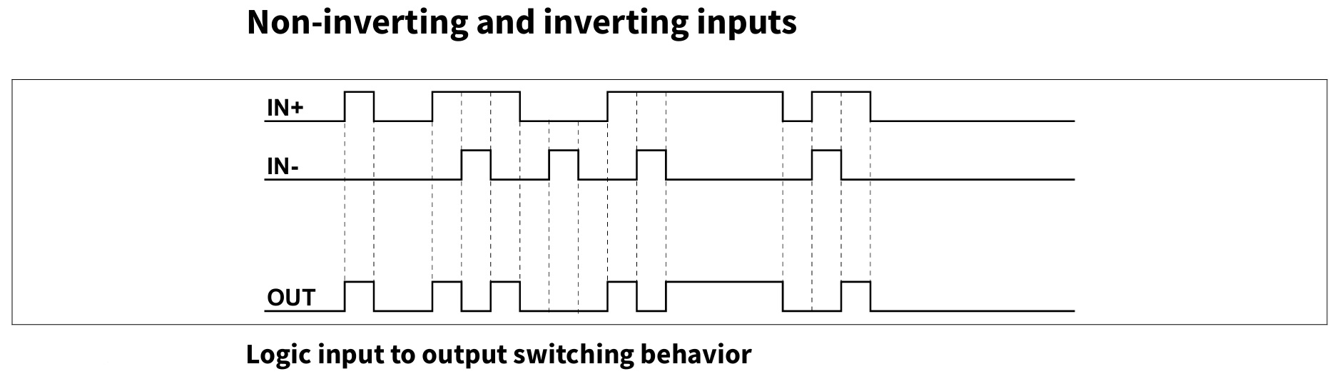
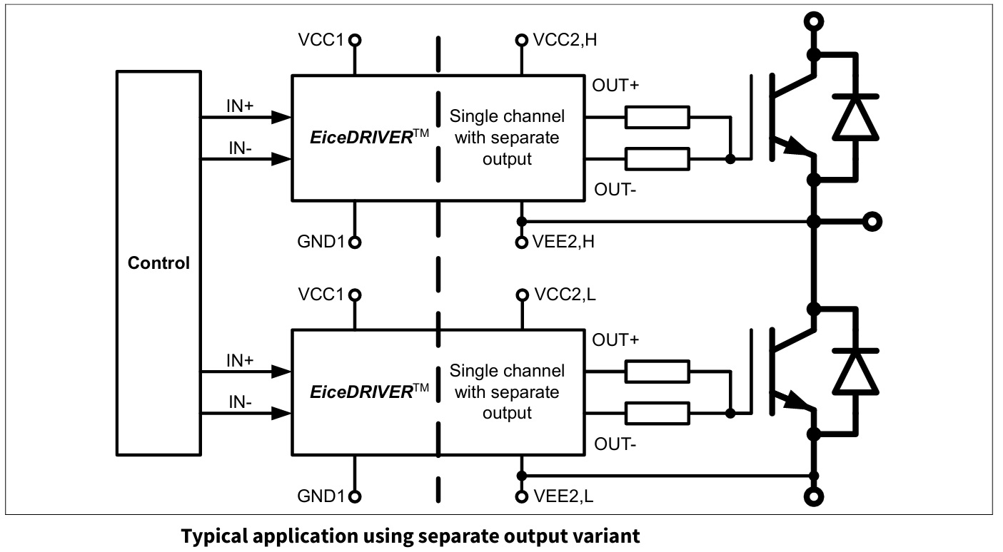
Logic input: for the output switching behavior there are two possible input modes to control the IGBT. At non-inverting mode IN+ controls the driver output while IN- is set to low. At inverting mode IN- controls the driver output while IN+ is set to high. A minimum input pulse width is defined to filter occasional glitches.
Driver outputs: The output driver section uses MOSFETs to provide a rail-to-rail output. This feature permits that tight control of gate voltage during on-state and short circuit can be maintained as long as the driver’s supply is stable. Due to the low internal voltage drop, switching behavior of the IGBT is predominantly governed by the gate resistor. Furthermore, it reduces the power to be dissipated by the driver.
Single-channel 5.7 kV (rms) isolated gate driver IC with separate output, Galvanically isolated coreless transformer gate driver, For use with 600 V/650 V/1200 V/1700 V/2300 V IGBTs
Features
- Input Supply 12V DC
- DC-DC Converter Output +15V DC/ -9V DC
- Header Connector for Input Power and Signal Input
- Up to 14.0 A typical peak output current
- DC-DC Converter Isolation 6.4VKVDC
- Gate Driver Chip Isolation 5.7 kV (rms)
- 3 V and 5 V input supply voltage
- High common-mode transient immunity CMTI > 200 kV/µs
- Output Header Connector
- On Board Power LED (Output DC-DC Converter)
- PCB Dimensions 31.12 x 23.81 mm
The module is configured for IGBTs but can also drive MOSFETs and Sic-MOSFETs by replacing the DC-DC converter with the following options:
- R12P22005D: +20/-5V for SiC MOSFETs
- R12P21503D: +15/-3V for SiC MOSFETs
- R12P21509D: +15/-9V for IGBTs
Board Can accommodate Lower Current Chips, few compatible chips list
- 1ED3120MC12H 5.5 A separate source and sink 8.0 V VDE + UL 3120MC12
- 1ED3121MC12H 5.5 A separate source and sink 10.5 V VDE + UL 3121MC12
- 1ED3123MC12H 14.0 A separate source and sink 8.0 V VDE + UL 3123MC12
- 1ED3124MC12H 14.0 A separate source and sink 10.5 V VDE + UL 3124MC12
- 1ED3131MC12H 5.5 A separate source and sink, 180 ns minimum input pulse suppression time
TRENCHSTOP IGBT Discrete (Compatible IGBTs)
- IKQ75N120CS6 High Speed 1200 V, 75 A IGBT with anti-parallel diode in TO247-3
- IKW15N120BH6 High Speed 1200 V, 15 A IGBT with anti-parallel diode in TO247
- IHW40N120R5 Reverse conducting 1200 V, 40 A IH IGBT with integrated diode in TO247
TRENCHSTOP IGBT Modules (Compatible IGBT Modules)
- F4-100R17N3E4 EconoPACK™ 3 1700 V, 100 A fourpack IGBT module
- F4-200R17N3E4 EconoPACK™ 3 1700 V, 200 A fourpack IGBT module
- FS150R17N3E4 EconoPACK™ 3 1700 V, 150 A sixpack IGBT module
- FF650R17IE4 PrimePACK™ 3 1700 V, 650 A half-bridge dual IGBT module
- FF1000R17IE4 PrimePACK™ 3 1700 V, 1000 A half-bridge dual IGBT module
- FF1200R17IP5 PrimePACK™ 3+ 1700 V, 1200 A dual IGBT module
- FF1500R17IP5 PrimePACK™ 3+ 1700 V, 1500 A dual IGBT module
- FF1500R17IP5R PrimePACK™ 3 1700 V, 1500 A dual IGBT module
- FF1800R17IP5 PrimePACK™ 3+ 1700 V, 1800 A dual IGBT module
- FP10R12W1T7_B11 EasyPIM™ 1B 1200 V, 10 A three phase input rectifier PIM IGBT module
- FS100R12W2T7_B11 EasyPACK™ 2B 1200 V, 100 A sixpack IGBT module
- FP150R12KT4_B11 EconoPIM™ 3 1200V three-phase PIM IGBT module
- FS200R12KT4R_B11 EconoPACK™ 3 1200 V, 200 A sixpack IGBT module
Applications
- AC and brushless DC motor drives
- High voltage DC-DC converter and DC-AC inverter
- Induction heating resonant application
- UPS-systems
- Commercial air-conditioning (CAC)
- Server and telecom switched mode power supplies (SMPS)
- Solar inverters, e.g. for 1500 V (DC) systems
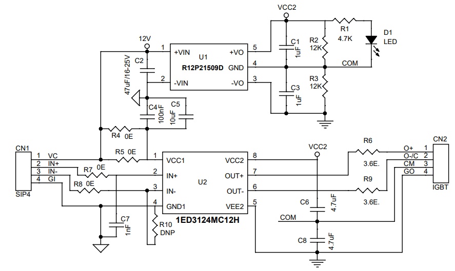
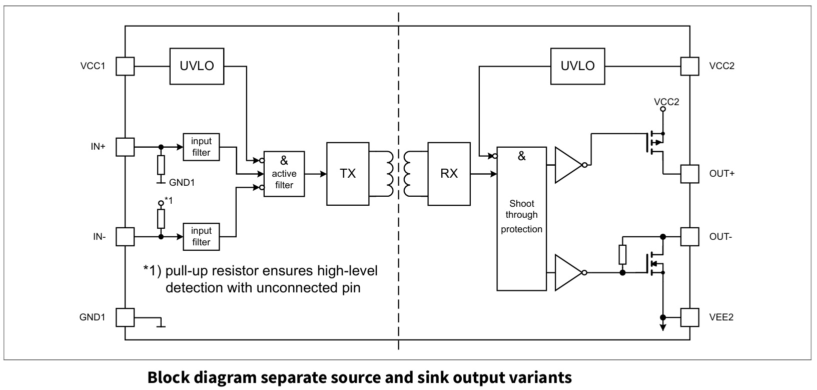
The 1ED3124MC12H gate driver ICs are galvanically isolated single channel gate driver ICs for IGBT, MOSFET and SiC MOSFET in PG-DSO-8 package. They provide a typical output current of up to 14.0 A on separate source and sink pins. The input logic pins operate on a wide input voltage range from 3 V to 15 V using CMOS threshold levels to support 3.3 V microcontrollers. Data transfer across the isolation barrier is realized by the coreless transformer technology. All variants have logic input and driver output undervoltage lockout (UVLO), and active shutdown.
Gate Driver Chip Pin description
- VCC1: Logic input supply voltage of 3.3 V up to 15 V wide operating range
- GND1: Ground connection of input circuit.
- IN+: non-inverted control signal for driver output. An internal filter provides robustness against noise at IN+. An internal weak pull-down resistor favors off-state.
- IN-: Inverted control signal for driver output. An internal filter provides robustness against noise at IN-. An internal weak pull-up resistor favors off-state.
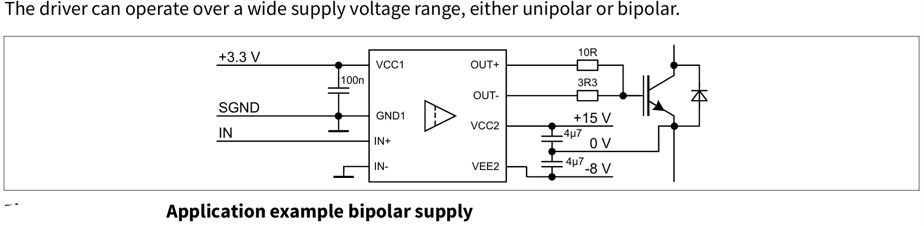
- VCC2: Positive power supply pin of output driving circuit. A proper blocking capacitor has to be placed close to this supply pin.
- VEE2: Reference ground of the output driving circuit. In case of a bipolar supply (positive and negative voltage referred to IGBT emitter) this pin is connected to the negative supply voltage.
- OUT+: Driver source output pin to turn on external IGBT. During on-state the driving output is switched to
- Switching of this output is controlled by IN+ and IN-. This output will also be turned off at an UVLO event.
- OUT-: Driver sink output pin to turn off external IGBT. During off-state the driving output is switched to VEE2.Switching of this output is controlled by IN+ and IN-. In case of UVLO an active shut down keeps the output voltage at a low level.
- OUT: Combined source and sink output pin to external IGBT. The output voltage will be switched between
- VCC2 and VEE2. Switching of this output is controlled by IN+ and IN-. In case of an UVLO event this output will be switched off and an active shut down keeps the output voltage at a low level.
Connections
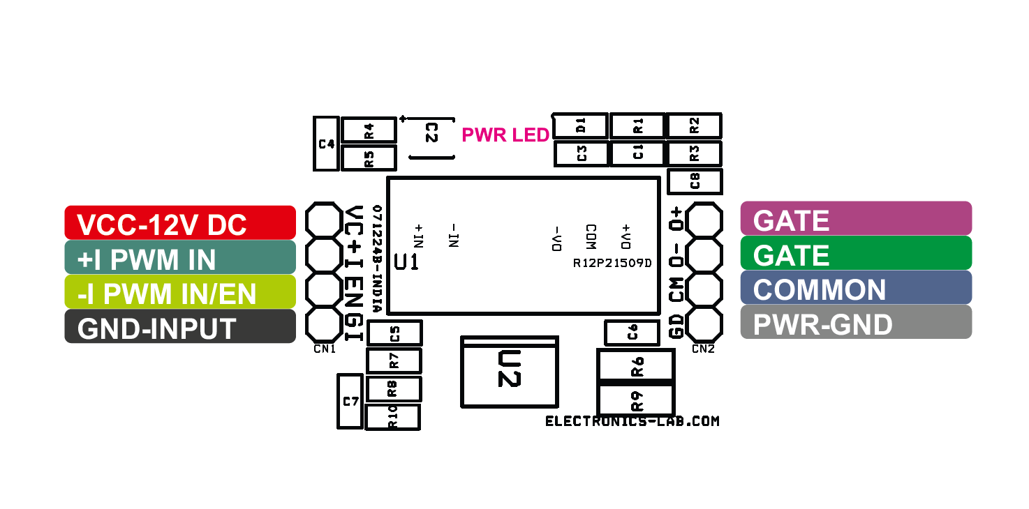
- CN1: Pin 1 = VCC 12V DC Input, Pin 2 = IN+ PWM Input, Pin 3 = IN- PWM Input, Pin 4 = GND-Input Side
- CN2: Pin 1 = IGBT Gate, Pin 2 = IGBT Gate, Pin 3 = Common (IGBT Emitter) , Pin 4 = Power Ground (No Use)
- D1: Power LED Output side
Schematic
Parts List
| NO. | QNTY. | REF. | DESC. | MANUFACTURER | SUPPLIER | SUPPLIER PART NO |
|---|---|---|---|---|---|---|
| 1 | 1 | CN1 | 4 PIN MALE HEADER PITCH 2.54MM | WURTH | DIGIKEY | 732-5317-ND |
| 2 | 1 | CN2 | 4 PIN MALE HEADER PITCH 2.54MM | WURTH | DIGIKEY | 732-5317-ND |
| 3 | 2 | C1,C3 | 1uF/35V CERAMIC SMD SIZE 0805 | YAGEO/MURATA | DIGIKEY | |
| 4 | 1 | C2 | 47uF/16-25V CERAMIC SMD SIZE 1210 | YAGEO/MURATA | DIGIKEY | |
| 5 | 1 | C4 | 100nF/50V CERAMIC SMD SIZE 0805 | YAGEO/MURATA | DIGIKEY | |
| 6 | 1 | C5 | 10uF/35V CERAMIC SMD SIZE 0805 | YAGEO/MURATA | DIGIKEY | |
| 7 | 2 | C6,C8 | 4.7uF/35V CERAMIC SMD SIZE 0805 | YAGEO/MURATA | DIGIKEY | |
| 8 | 1 | C7 | 1nF/50V CERAMIC SMD SIZE 0805 | YAGEO/MURATA | DIGIKEY | |
| 9 | 1 | D1 | LED SMD SIZE 0805 | OSRAM | DIGIKEY | 475-1278-1-ND |
| 10 | 1 | R1 | 4.7K 5% SMD SIZE 0805 | YAGEO/MURATA | DIGIKEY | |
| 11 | 2 | R2,R3 | 12K 5% SMD SIZE 0805 | YAGEO/MURATA | DIGIKEY | |
| 12 | 4 | R4,R5,R7,R8 | 0E SMD SIZE 0805 | YAGEO/MURATA | DIGIKEY | |
| 13 | 2 | R6,R9 | 3.6E 5% SMD SIZE 1206 | YAGEO/MURATA | DIGIKEY | |
| 14 | 1 | R10 | DNP | |||
| 15 | 1 | U1 | R12P21509D | RECOM POWER | DIGIKEY | 945-2800-ND |
| 16 | 1 | U2 | 1ED3124MC12H | INFINEON | DIGIKEY | 448-1ED3124MC12HXUMA1CT-ND |
Connections
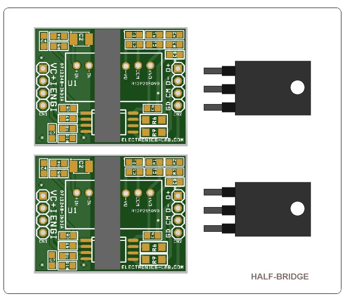
Half Bridge Configuration
Application Diagram
Power Supply Options

Block Diagram
IC Pinout

Input Waveforms