High Voltage IGBT Module, Low-side Driver with Over-Current Protection and Fault/Enable
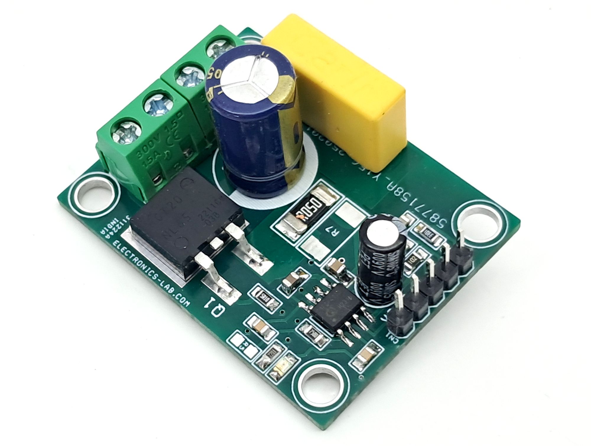
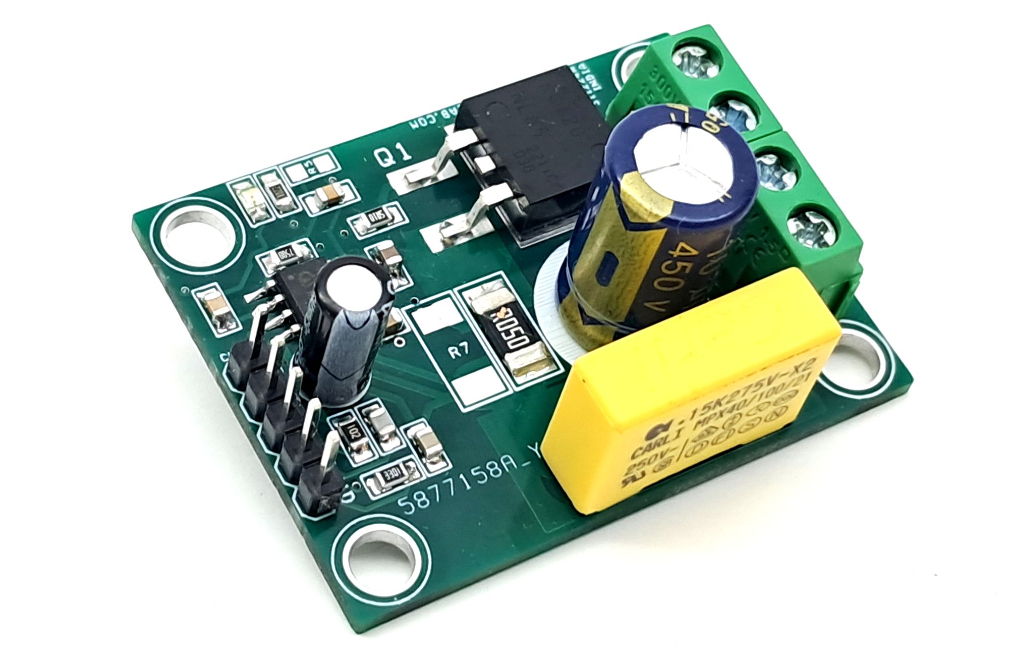
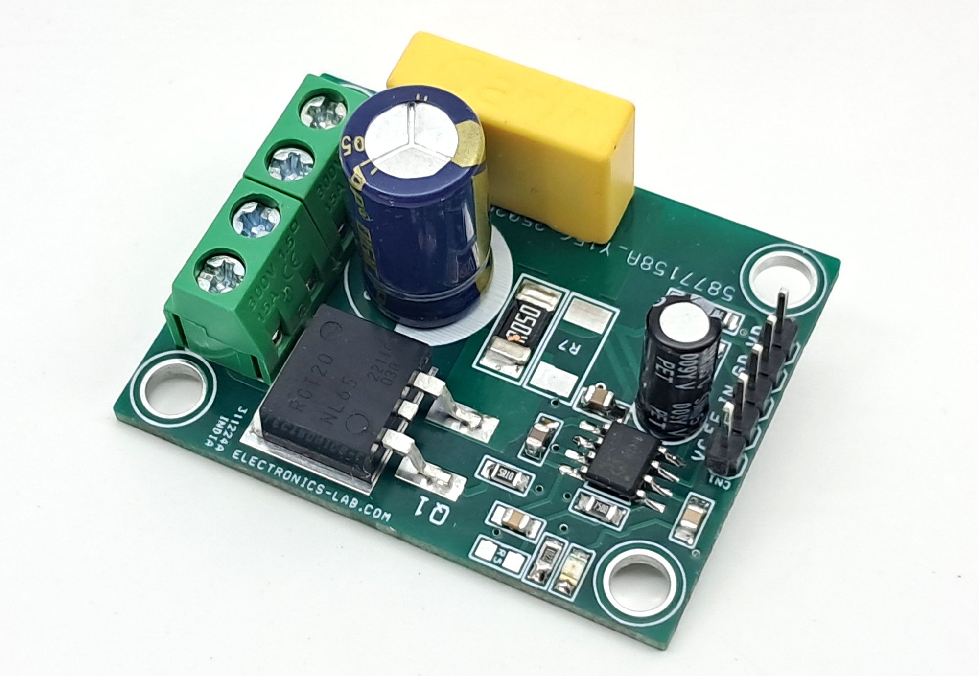
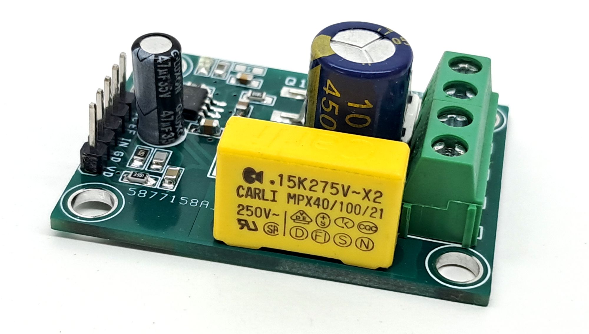
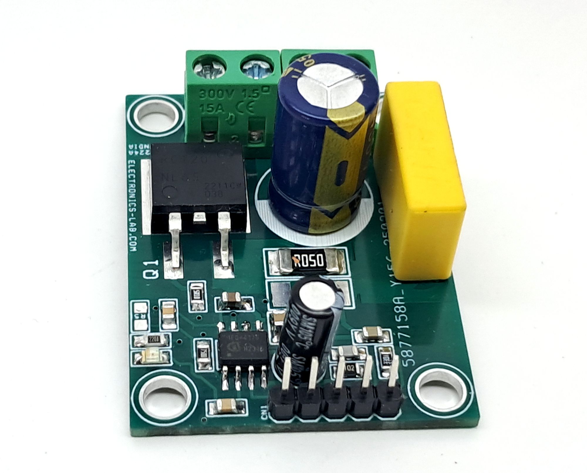
This IGBT driver module is a low-side gate driver that features integrated over-current protection. The primary functions of this module are its built-in over-current protection and enable/fault output capabilities. The board’s main components include the gate driver chip (1ED44176N01F), an SMD D2PK IGBT, and a current sense resistor. The chip is equipped with an over-current protection function, which has a typical threshold of 0.5V at the OCP (Over-Current Protection) point. When an over-current condition occurs, the driver output is automatically switched off. Simultaneously, the EN/FLT (Enable/Fault) pin is internally pulled down, and an internal current source charges the capacitor (C4) connected between the FLTC and VSS pins to program the fault clear time. This module is capable of driving loads up to 1A and can drive higher current with forced air cooling. It can operate within a load power supply range of 80-400V DC, making it a reliable and efficient solution for various applications.
This IGBT driver module is a low-side gate driver that features integrated over-current protection. The primary functions of this module are its built-in over-current protection and enable/fault output capabilities. The board’s main components include the gate driver chip (1ED44176N01F), an SMD D2PK IGBT, and a current sense resistor. The chip is equipped with an over-current protection function, which has a typical threshold of 0.5V at the OCP (Over-Current Protection) point. When an over-current condition occurs, the driver output is automatically switched off. Simultaneously, the EN/FLT (Enable/Fault) pin is internally pulled down, and an internal current source charges the capacitor (C4) connected between the FLTC and VSS pins to program the fault clear time. This module is capable of driving loads up to 1A and can drive higher current with forced air cooling. It can operate within a load power supply range of 80-400V DC, making it a reliable and efficient solution for various applications.
Features
- Power Supply for the Load 80V to 400V DC
- Power Supply for Logic Circuit 15V (Range 12V-16V)
- Load Current Up To 1A, Higher Current with Cooling Fan
- Power Supply VD(VDD) 3.3V To 5V
- On Board Power LED
- Header Connector for Gate Driver Power and Input/Output Signal
- Screw Terminals for Load Power and Load
- Over-current detection with positive voltage input (OC shutdown)
- 5 V over-current threshold with accurate ±5% tolerance
- Single pin for fault output and enable, Normally High
- Under voltage lockout
- CMOS Schmitt-triggered Inputs
- 3 V, 5 V and 15 V Input Logic Compatible
- Output in Phase with Input
- VCC Supply Undervoltage Positive Going Threshold 11.9V
- OCP to Low Level EN/FLT Signal Delay 440nS
- Fault Clear Time 110uS (C4=1nF)
- The switch turns off during protection
- PCB Dimensions 44.61 x 33.97mm
- 4 x 4MM PCB Mounting Holes
Potential applications
- Digitally controlled PFC
- Heater Controller
- High Voltage Boost DC-DC Converter
- Air conditioner
- Home appliances
- Industrial applications
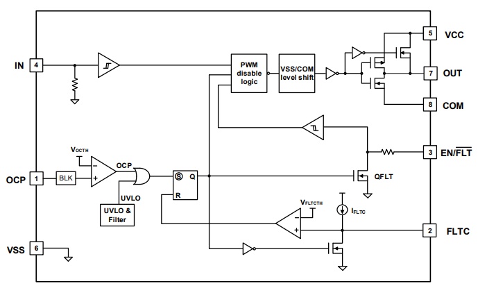
The 1ED44176N01F is a low-voltage, power MOSFET and IGBT non-inverting gate driver. Proprietary latch immune CMOS technologies enable ruggedized monolithic construction. The logic input is compatible with standard CMOS or LSTTL output. The output driver features a current buffer stage. The 1ED44176N01F has OCP pin for over current protection sense and a FAULT status output (Once it is active, EN/FLT pin is internally pulled down.). There is a dedicated pin (FLTC) to program fault clear time. The EN/FLT needs to be outside pulled up to provide normal operation, pulling EN/FLT low disable the driver. Internal circuitry on VCC pin provides an under-voltage lockout protection that holds output low until Vcc supply voltage is within operating range.
Block Diagram
Typical Application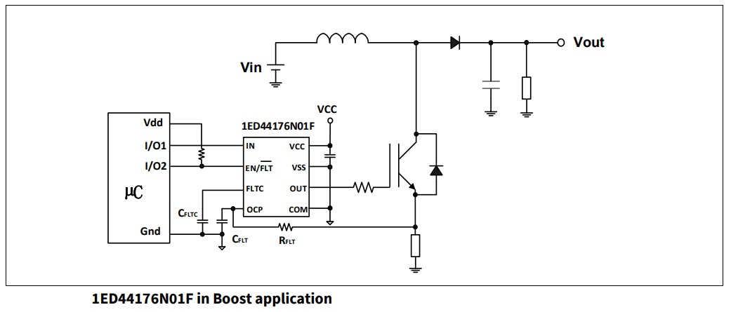
Input logic compatibility
The input of this IC is compatible with standard CMOS and TTL outputs. The 1ED44176N01F has been designed to be compatible with 3.3 V, 5 V and 15 V logic-level signals. The input high threshold (VINH) is typ. 2.1 V and low threshold (VINL) is typ. 1 V. Input hysteresis offers enhanced noise immunity. The 1ED44176N01F includes an important feature: wherein, whenever the input pin is in a floating condition, the output is held in the low state. This is achieved using GND pull-down resistors on the input pin.
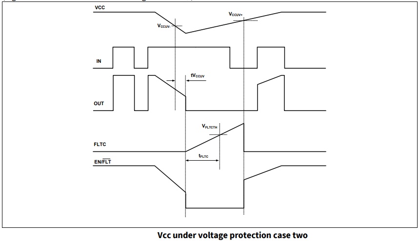
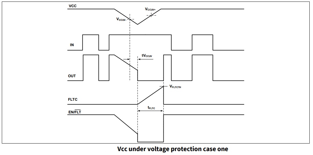
Undervoltage lockout (VCC)
The 1ED44176N01F has an internal UVLO protection feature on the VCC pin supply circuit blocks. Upon power-up, if the VCC voltage fails to reach the VCCUV+ threshold, the driver cannot turn on. Additionally, if the VCC voltage decreases below the VCCUV- threshold and the VCC bias voltage remains lower than the VCCUV- threshold exceeding UVLO filter time (tVCCUV) during operation, the undervoltage lockout circuitry will recognize a fault condition and shut-down the drive output. The EN/FLT will then transit to the low state to inform the controller of the fault condition, regardless of the status of the IN-input pin. The tVCCUV about 2μs helps to suppress noise from the UVLO circuit, so that negative-going voltage spikes at the supply pin will avoid parasitic UVLO events. When VCC is higher than VCCUV+ and longer than tFLTC, EN/FLT becomes high and the OUT will follow the input signal IN.
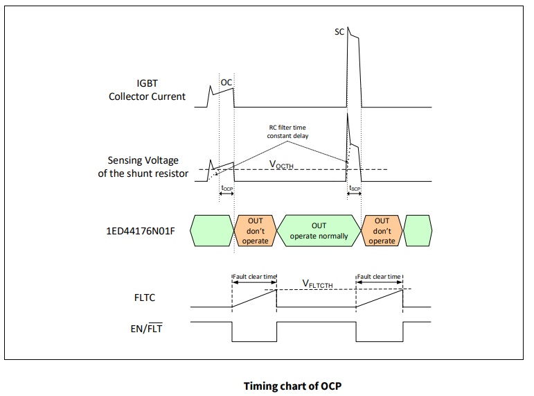
Over current protection (OCP)
The 1ED44176N01F has a function of over current protection with a threshold VOCTH at the OCP pin. The voltage at this pin is the voltage across the current sense resistor. To avoid false tripping due to the fast high current switch on transient that occurs at the switch on of MOSFET or IGBT resulting from the circuit parasitic capacitors, there is blanking interval which disables over current detection for the period of tBLK. (An additional RC filter is recommended, if the internal tBLK is not sufficient to suppress the noise.) After tBLK and the voltage of OCP pin is over VOCTH, the 1ED44176N01F causes fault logic to initiate a fault shutdown sequence. This sequence starts with the generation of a fault signal. The internal MOSFET QFLT is turned on and EN/FLT pin is pulled down.
The value of the RCS R6 (Current Sense Resistor) is calculated by the following equation: RSC= V Over Current Threshold/Over Current
RSC= 0.5V/10 = 50m Ohm (0.05 Ohms)
Fault Reporting and Programmable Fault Clear Timer
The 1ED44176N01F provides a dedicated fault reporting output pin (EN/FLT) and a programmable fault clear time pin (FLTC). There are two situations which would cause the driver to report a fault via the EN/FLT pin. The first is an under-voltage condition of VCC and the second is if the OCP pin recognizes a fault. Once the fault condition occurs, the EN/FLT pin is internally pulled down to VSS. The EN/FLT output stays in the low state until the fault condition has been removed and the fault clear timer expires; once the fault clear timer expires, the voltage on the EN/FLT pin will return to its external pull-up voltage. The length of the fault clear time period (tFLTC) is programmed by external capacitor C4 which connected between FLTC and VSS (CFLTC). The length of the fault clear time period can be determined by using the equation below. tFLTC= CFLTC*VFLTCTH/ IFLTC
Enable Input
1ED44176N01F provides an enable functionality that allows to shut down or to enable the output. When EN/FLT is pulled up (the enable voltage is higher than VENH) the output is able to operate normally, pulling EN/FLT low (the enable voltage is lower than VENL) the output is disable. The enable function is not latched. The relationships between the input, output.
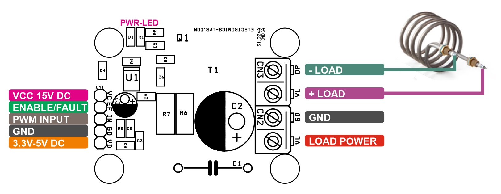
Testing Conditions
- Load Power Supply 110V/5Amps
- Gate Driver Power Supply 15V/1Amp
- Enable = 5V from Arduino Uno Power
- Input Signal 20Khz, 50% Duty Cycle, TTL 5V (Arduino Uno), Arduino Code Available as download
- Load 100 Ohms 10W Resistor
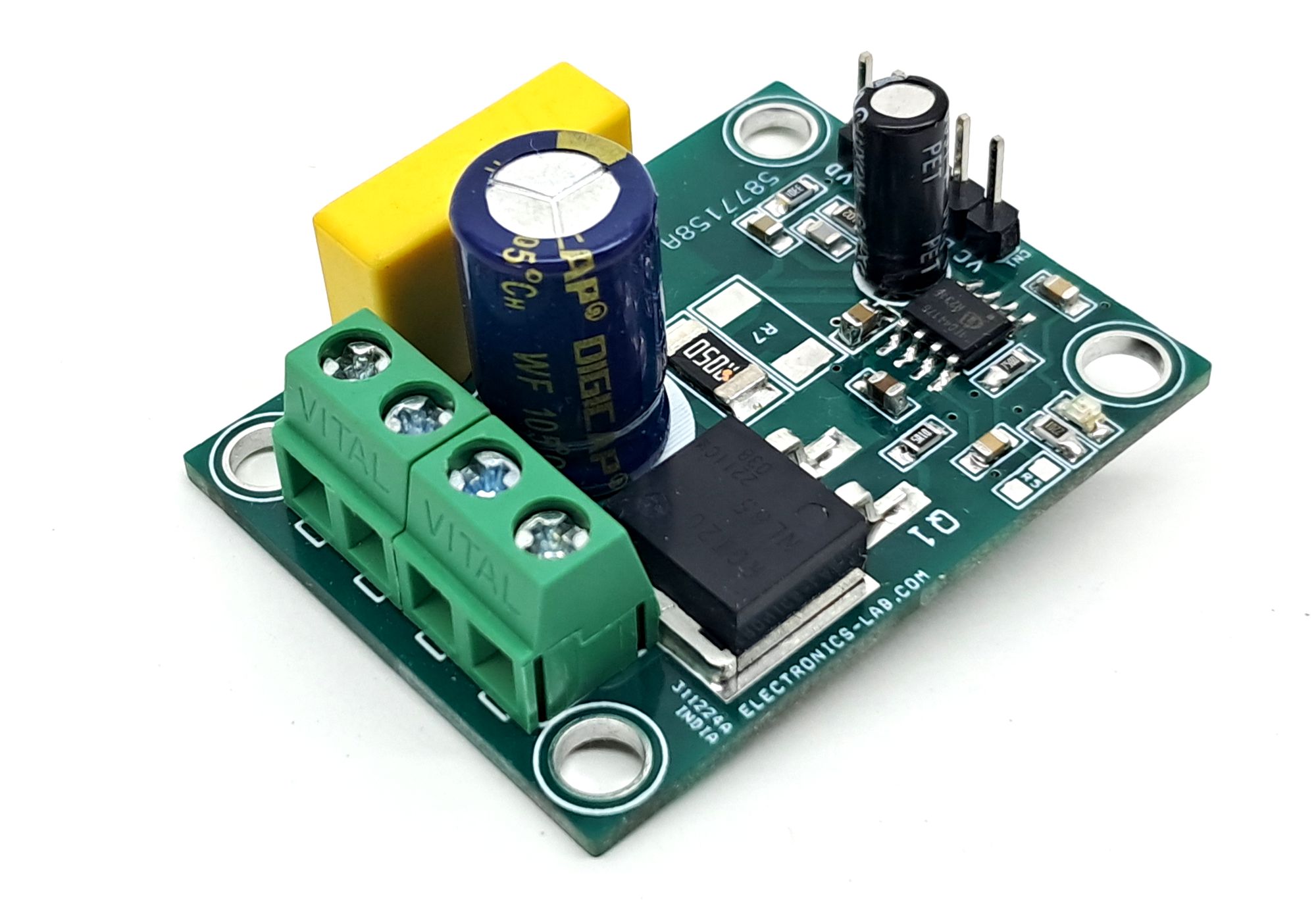
Connections
- CN1: Pin 1 = VCC 12V-16V, Pin 2 = Enable/Fault, Pin 3 = PWM/Signal Input, Pin 4 GND, Pin 5 = VDD 3.3V-5V DC
- CN2: Pin 1 = Load Power 80V-400VD, Pin 2 = GND
- CN3: Pin 1 = +Load, Pin 2 = -Load
- D1: Power LED
Schematic
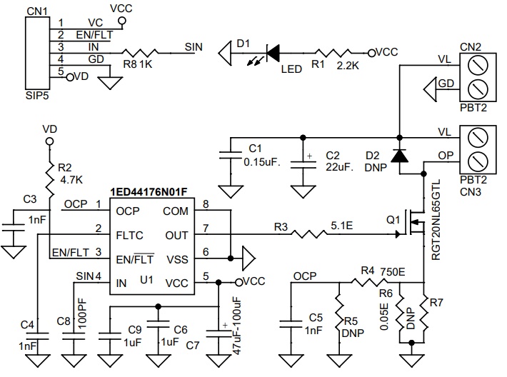
Parts List
| NO. | QNTY. | REF. | DESC. | MANUFACTURER | SUPPLIER | SUPPLIER PART NO |
|---|---|---|---|---|---|---|
| 1 | 1 | CN1 | 5 PIN MALE HEADER PITCH 2.54MM | WURTH | DIGIKEY | 732-5318-ND |
| 2 | 2 | CN2,CN3 | 2 PIN SCREW TERMINAL PITCH 5.08MM | PHOENIX | DIGIKEY | 277-1247-ND |
| 3 | 1 | C1 | 0.15uF/275VX2 | PANASONIC | DIGIKEY | P14787-ND |
| 4 | 1 | C2 | 22uF/450V DC (DIA 12.5MM) | RUBYCON | DIGIKEY | 1189-2936-ND |
| 5 | 3 | C3,C4,C5 | 1nF/50V CERAMIC SMD SIZE 0805 | YAGEO/MURATA | DIGIKEY | |
| 6 | 2 | C6,C9 | 1uF/50V CERAMIC SMD SIZE 0805 | YAGEO/MURATA | DIGIKEY | |
| 7 | 1 | C7 | 100uF/25V (DIA5MM) | KEMET | DIGIKEY | 399-6102-ND |
| 8 | 1 | C8 | 100PF/50V CERAMIC SMD SIZE 0805 | YAGEO/MURATA | DIGIKEY | |
| 9 | 1 | D1 | LED RED SMD SIZE 0805 | OSRAM | DIGIKEY | 475-1278-1-ND |
| 10 | 3 | D2,R5,R7 | DNP | |||
| 11 | 1 | Q1 | RGT20NL65GTL D2PK | ROHM | DIGIKEY | 846-RGT20NL65GTLCT-ND |
| 12 | 1 | R1 | 2.2K 5% SMD SIZE 0805 | YAGEO/MURATA | DIGIKEY | |
| 13 | 1 | R2 | 4.7K 5% SMD SIZE 0805 | YAGEO/MURATA | DIGIKEY | |
| 14 | 1 | R3 | 5.1E 5% SMD SIZE 0805 | YAGEO/MURATA | DIGIKEY | |
| 15 | 1 | R4 | 750E 5% SMD SIZE 0805 | YAGEO/MURATA | DIGIKEY | |
| 16 | 1 | R6 | 0.05E/1-3W 1% SMD SIZE 2512 | STACKPOLE | DIGIKEY | CSRN2512FK50L0 |
| 17 | 1 | R8 | 1K 5% SMD SIZE 0805 | YAGEO/MURATA | DIGIKEY | |
| 18 | 1 | U1 | 1ED44176N01F | INFINEON | DIGIKEY | 448-1ED44176N01FXUMA1CT-ND |
Connections
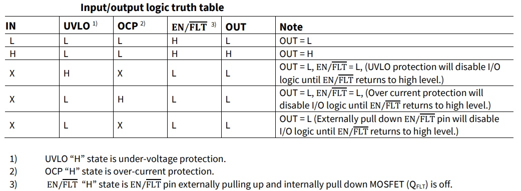
Input – Output Table
OCP Fault Clear Function
![]()
OCP Timing Diagram
VCC Undervoltage Protection Diagrams
Gerber View
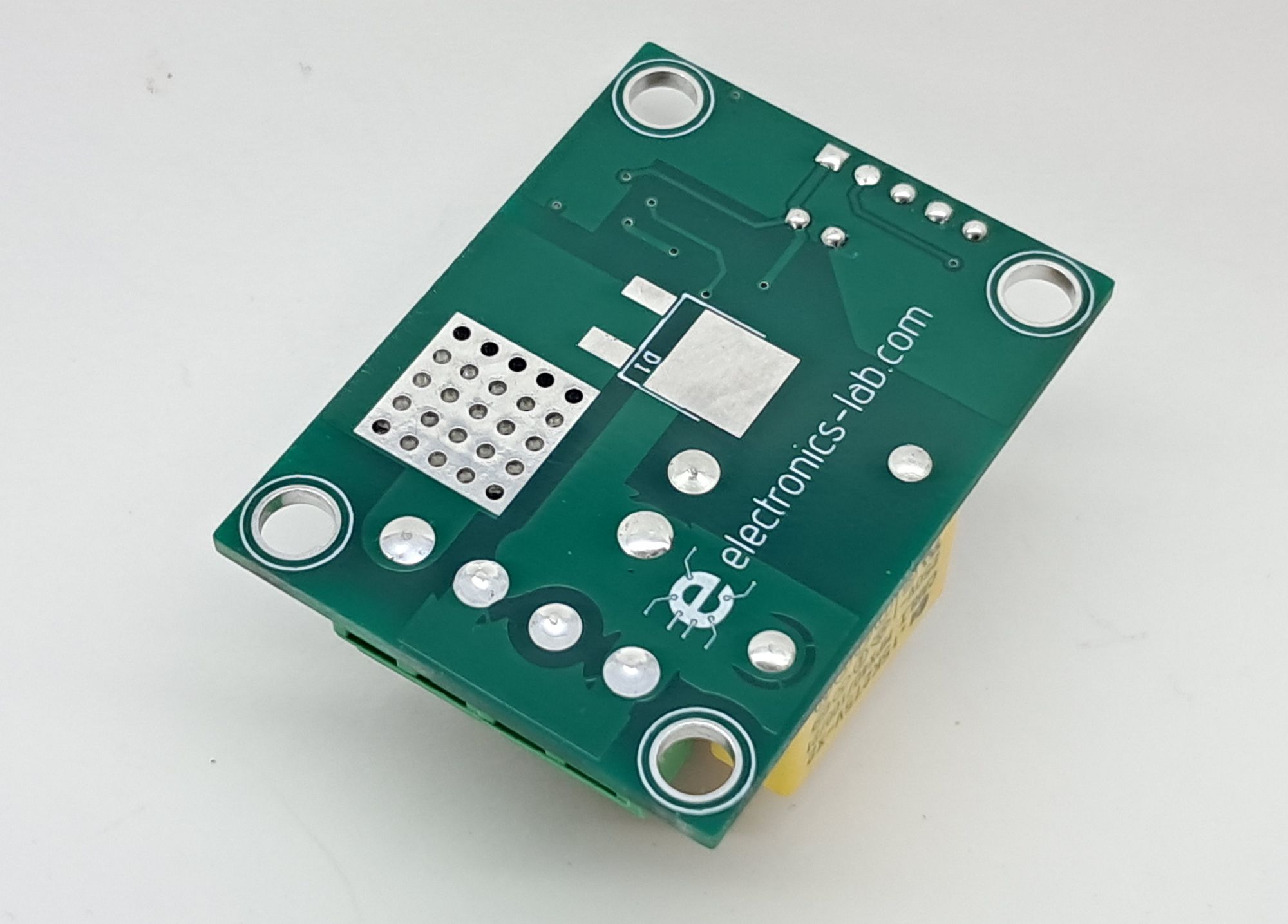
Photos