Precision Digital Current and Power Monitor using INA260
This module is a digital-output monitor (INA260) that measures current, power, and voltage via an I2C/SMBus interface. It includes a precision shunt resistor for high-accuracy, bidirectional measurement across a common-mode voltage range of 0V to 36V.
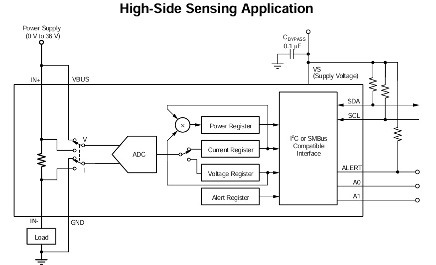
This is a digital-output, current, power, and voltage monitor with an I2C and SMBus™-compatible interface with an integrated precision shunt resistor. It enables high-accuracy current and power measurements and over-current detection at common-mode voltages that can vary from 0 V to 36 V, independent of the supply voltage. Module is a bidirectional, low- or high-side, current-shunt monitor that measures current flowing through the internal current-sensing resistor. The integration of the precision current-sensing resistor provides calibration-equivalent measurement accuracy with ultra-low temperature drift performance and ensures that an optimized Kelvin layout for the sensing resistor is always obtained.
The INA260 features up to 16 programmable addresses on the I2C-compatible interface. The digital interface allows programmable alert thresholds, analog-to-digital converter (ADC) conversion times, and averaging. To facilitate ease of use, an internal multiplier enables direct readouts of current in amperes and power in watts.
Features
- Operates From a 2.7-V to 5.5-V Power Supply
- Precision Integrated Shunt Resistor
- Current Sense Resistance: 2 mΩ
- Tolerance Equivalent to 0.1%
- 15-A Continuous From –40°C to +85°C
- 10 ppm/°C Temperature Coefficient (0°C to +125°C)
- Senses Bus Voltages From 0 V to 36 V
- High-Side or Low-Side Sensing
- Reports Current, Voltage, and Power
- High Accuracy:0.15% System Gain Error (Maximum),5-mA Offset (Maximum)
- Configurable Averaging Options
- 16 Programmable Addresses
- PCB Dimensions 36.20 x 23.34 mm
- 4 x 4MM Mounting Holes
Integrated Shunt Resistor
SDA SCL ALERT A0 A1 The INA260 features a precise, low-drift, current-sensing resistor to allow for precision measurements over the entire specified temperature range of–40°C to +125°C. The integrated current-sensing resistor ensures measurement stability over temperature as well as simplifying printed-circuit board (PCB) layout difficulties common in high precision current sensing measurements. The onboard current-sensing resistor is designed as a 4-wire (or Kelvin) connected resistor that enables accurate measurements through a force-sense connection. The Kelvin connections to the shunt are done internally eliminating many of the parasitic impedances commonly found in typical very-low sensing-resistor level measurements. Although the shunt resistor can be accessed through the IN+ and IN– pins, this resistor is not intended to be used as a stand-alone component. The INA260 is internally calibrated to ensure that the current sensing resistor and current-sensing amplifier are both precisely matched to one another. The INA260 has approximately 4.5 mΩ of total resistance between the IN+ and IN- pins. 2 mΩ of this total package resistance is a precisely-controlled resistance from the Kelvin-connected current-sensing resistor used by the internal analog to digital converter (ADC). The power dissipation requirements of the system and package are based on the total 4.5-mΩ package resistance. The heat dissipated across the package when current flows through the device ultimately determines the maximum current that can be safely handled by the package. The current consumption of the silicon is relatively low, leaving the total package resistance carrying the high load current as the primary contributor to the total power dissipation of the package. The maximum safe-operating current level is set to ensure that the heat dissipated across the package is limited so that no damage to the resistor or the package itself occurs or that the internal junction temperature of the silicon does not exceed a 150°C limit.
ALERT Pin
The INA260 has a single Alert Limit Register (07h), that allows the ALERT pin to be programmed to respond to a single user-defined event or to a Conversion Ready notification if desired. The Mask/Enable Register allows the user to select from one of the five available functions to monitor as well as setting the Conversion Ready bit to control the response of the ALERT pin. Based on the function being monitored, enter a value into the Alert Limit Register to set the corresponding threshold value that asserts the ALERT pin. The ALERT pin allows for one of several available alert functions to be monitored to determine if a user-defined threshold has been exceeded. The five alert functions that can be monitored are: • Shunt Over Current-Limit (OCL) • Shunt Under Current-Limit (UCL) • BusVoltage Over-Limit (BOL) • BusVoltage Under-Limit (BUL) • Power Over-Limit (POL) The ALERT pin is an open-drain output. This pin is asserted when the alert function selected in the Mask/Enable Register exceeds the value programmed into the Alert Limit Register. Only one of these alert functions can be enabled and monitored at a time. If multiple alert functions are enabled, the selected function in the highest significant bit position takes priority and responds to the Alert Limit Register value. For example, if the shunt over and under current limit functions are both selected, the Alert pin asserts when the shunt current exceeds the value in the Alert Limit Register. The Conversion Ready state of the device can also be monitored at the ALERT pin to inform the user when the device has completed the previous conversion and is ready to begin a new conversion. Conversion Ready can be monitored at the ALERT pin along with one of the alert functions. If an alert function and the Conversion Ready are both enabled to be monitored at the ALERT pin, after the ALERT pin is asserted, the Mask/Enable Register must be read following the alert to determine the source of the alert. By reading the Conversion Ready Flag (CVRF, bit 3), and the Alert Function Flag (AFF, bit 4) in the Mask/Enable Register, the source of the alert can be determined. If the Conversion Ready feature is not desired and the CNVR bit is not set, the ALERT pin only responds to an exceeded alert limit based on the alert function enabled.
Communications Bus Overview
The INA260 offers compatibility with both I2C and SMBus interfaces. The I2C and SMBus protocols are essentially compatible with one another. The I2C interface is used throughout this data sheet as the primary example, with SMBus protocol specified only when a difference between the two systems is discussed. Two lines, SCL and SDA, connect the device to the bus. Both SCL and SDA connect to the bus and require external pullup resistors. The device that initiates a data transfer is called a master, and the devices controlled by the master are slaves. The bus must be controlled by a master device that generates the serial clock (SCL), controls the bus access, and generates START and STOP conditions. The SCL pin on the INA260 is an input only and will not stretch the clock by holding the clock line low. To address a specific device, the master initiates a start condition by pulling the data signal line (SDA) from a high to a low logic level while SCL is high. All slaves on the bus shift in the slave address byte on the rising edge of SCL, with the last bit indicating whether a read or write operation is intended. During the ninth clock pulse, the slave being addressed responds to the master by generating an Acknowledge and pulling SDA low. Data transfer is then initiated and eight bits of data are sent, followed by an Acknowledge bit. During data transfer, SDA must remain stable while SCL is high. Any change in SDA while SCL is high is interpreted as a start or stop condition. After all data have been transferred, the master generates a stop condition, indicated by pulling SDA from low to high while SCL is high. The device includes a 28-ms timeout on its interface to prevent locking up the bus.
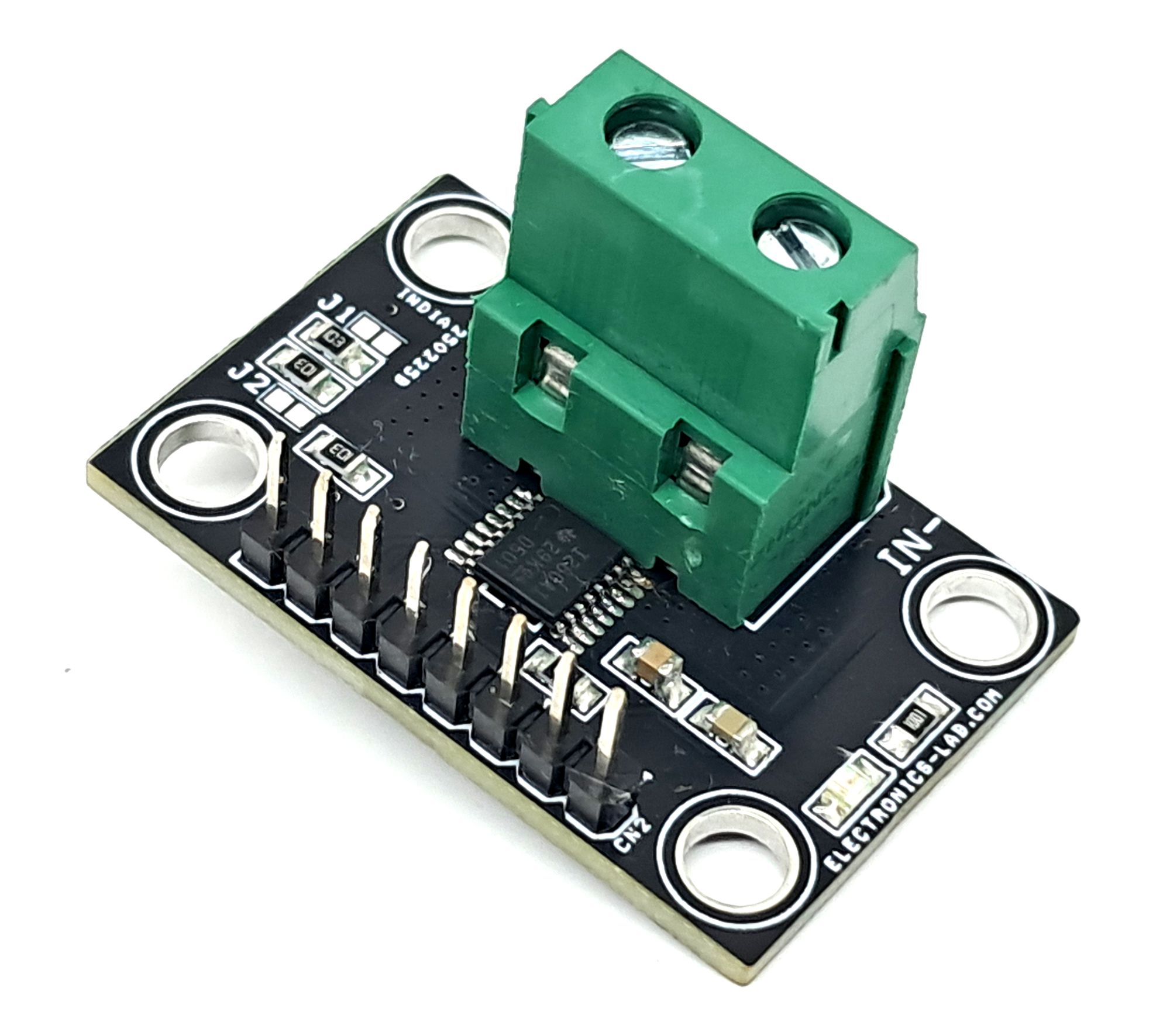
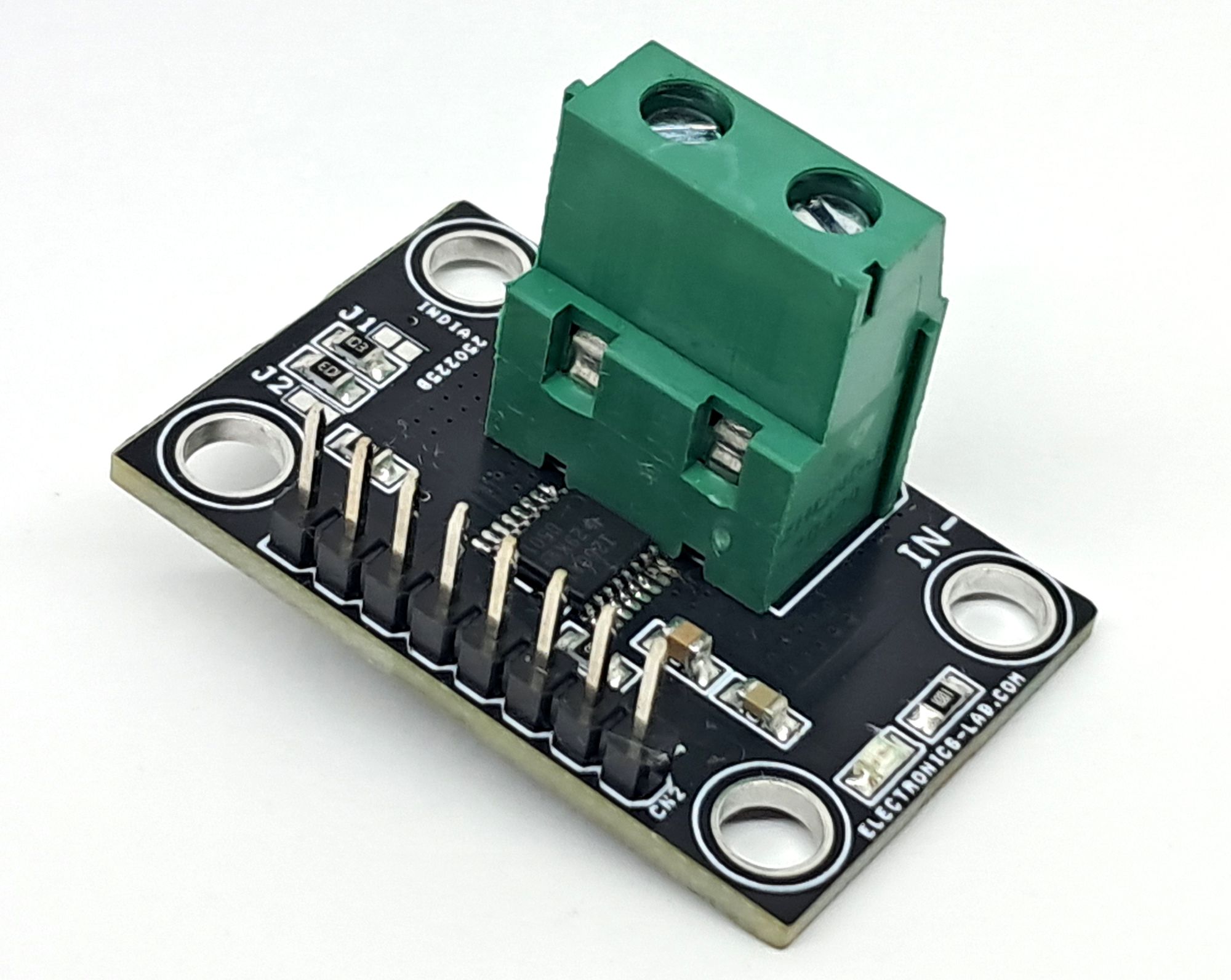
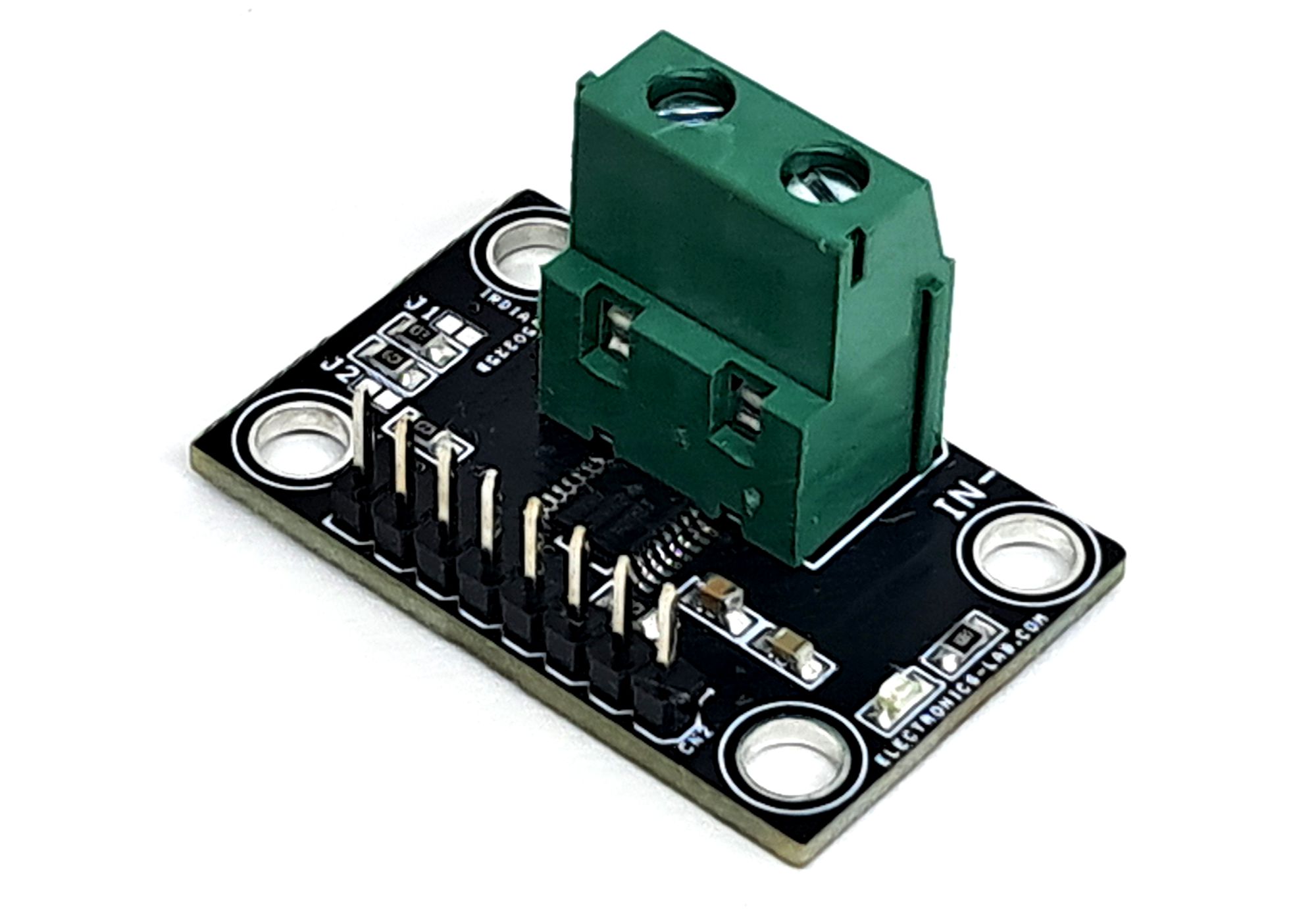
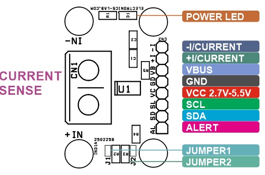
Connections
- CN1: Pin 1 = +IN/Current Sense, Pin 2 = -IN/Current Sense
- CN2: Pin 1 = Alert, Pin 2 = SDA, Pin 3 = SCL, Pin 4 = VCC, Pin 5 = GND, Pin 6 = VBUS, Pin 7 = +IN, Pin 8 = -IN
- Jumper 1, Jumper 2: Solder Type, Address Jumpers
- D1: Power LED
Schematic

Parts List
| NO | QNTY. | REF | DESC. | MANUFACTURER | SUPPLIER | SUPPLIER PART NO |
|---|---|---|---|---|---|---|
| 1 | 1 | CN1 | 2 PIN SCREW TERMINAL PITCH 7.62MM | WURTH | DIGIKEY | 732-10975-ND |
| 2 | 1 | CN2 | 8 PIN MALE HEADER PITCH 2.54MM | WURTH | DIGIKEY | 732-5321-ND |
| 3 | 1 | C1 | 10uF/16V CERAMIC SMD SIZE 0805 | YAGEO/MURATA | DIGIKEY | |
| 4 | 1 | C2 | 100nF/50V CERAMIC SMD SIZE 0805 | YAGEO/MURATA | DIGIKEY | |
| 5 | 1 | D1 | LED RED SMD SIZE 0805 | OSRAM | DIGIKEY | 475-1278-1-ND |
| 6 | 2 | J1,J2 | JUMPER SOLDER TYPE/PCB | |||
| 7 | 1 | R1 | 1K 5% SMD SIZE 0805 | YAGEO/MURATA | DIGIKEY | |
| 8 | 4 | R2,R3,R4,R5 | 10K 5% SMD SIZE 0805 | YAGEO/MURATA | DIGIKEY | |
| 9 | 1 | U1 | INA260 16TSSOP | TI | DIGIKEY | 296-47777-1-ND |
Connections
Application Diagram
Gerber View
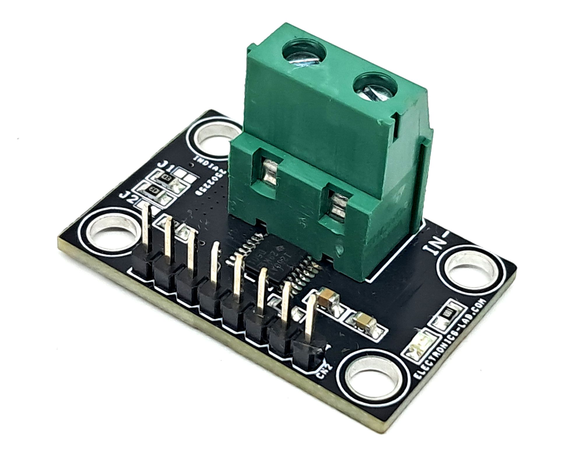
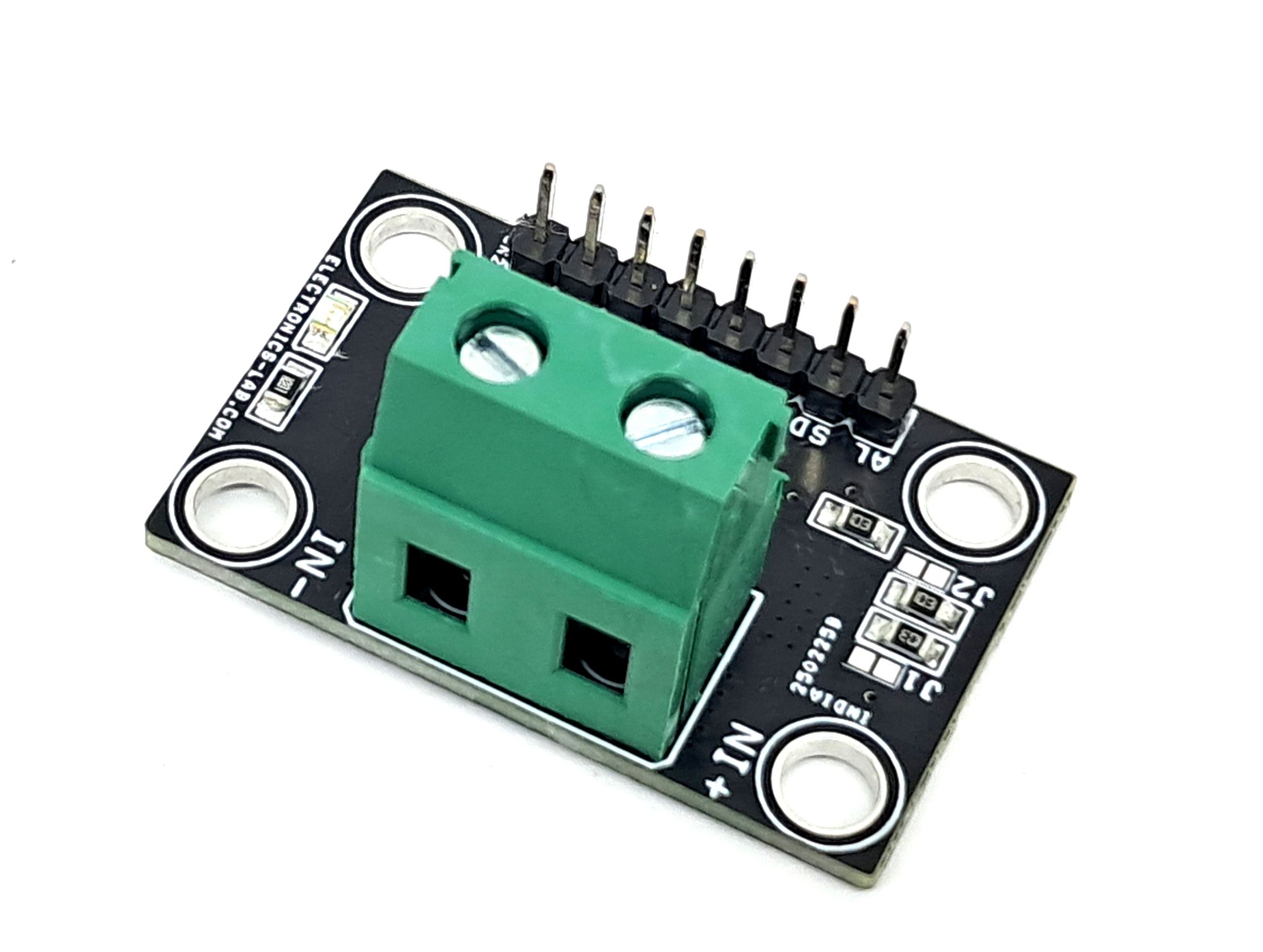
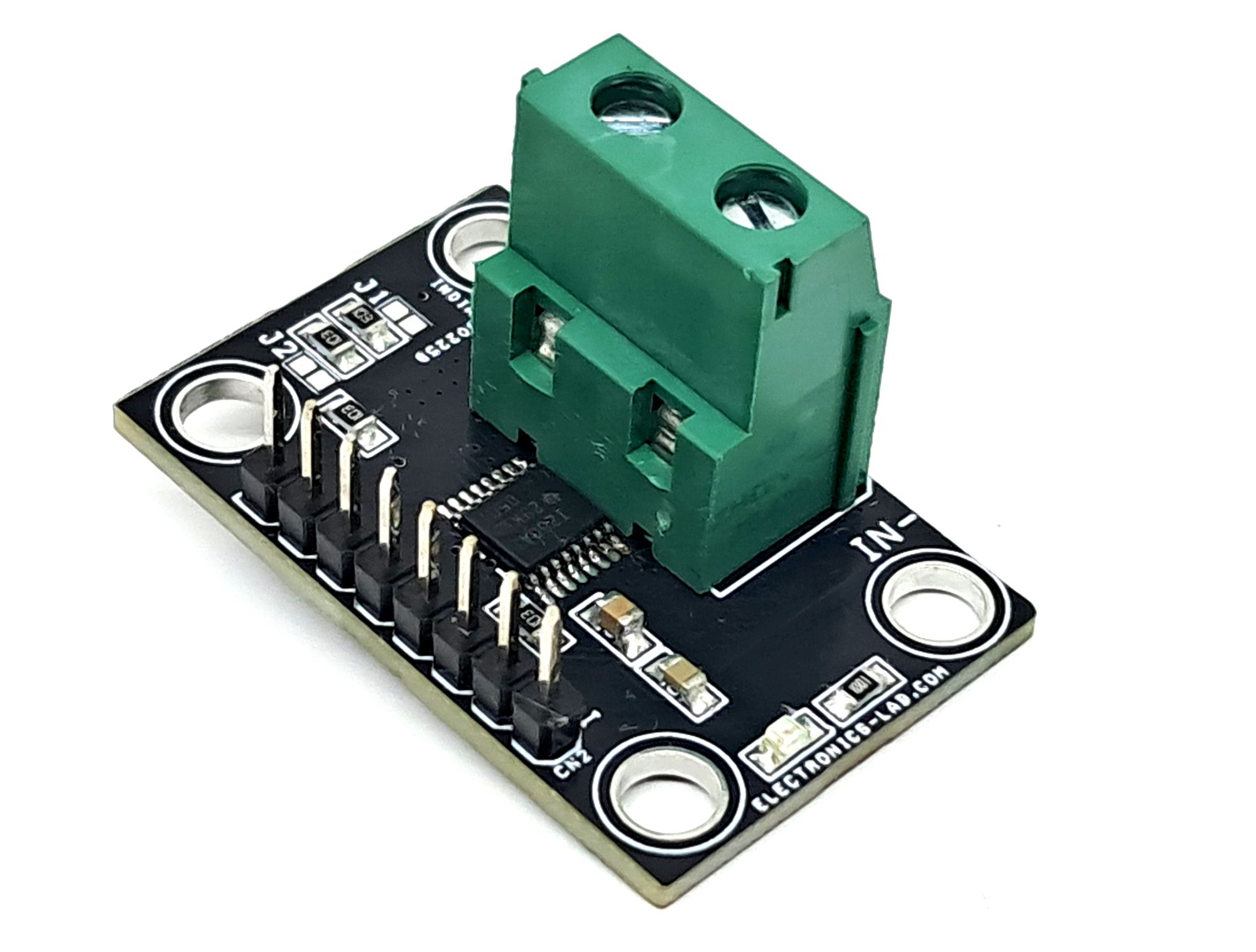
Photos