Solenoid & DC Motor Driver Shield for OLEDUINO v2
OLEDUINO-V2 Shield is able to drive up to 3.7A/24V for motors & solenoids. PWM control with sleep and back-EMF brake modes.
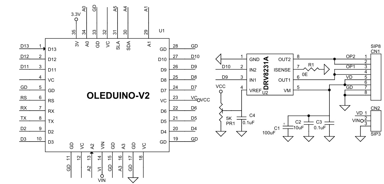
This power driver shield is designed to drive solenoids or brushed DC motors using the OLEDUINO-V2 platform. The driver can handle peak currents of up to 3.7A and supports a DC supply voltage of up to 24Vdc.
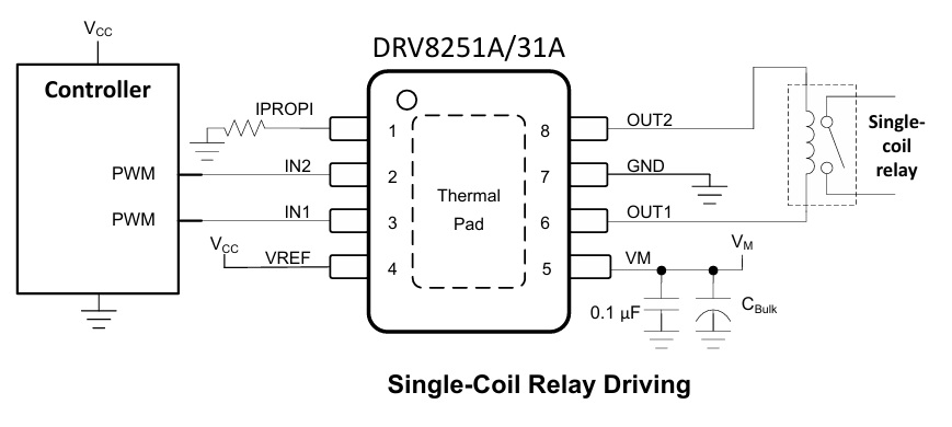
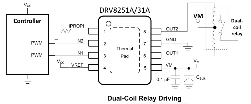
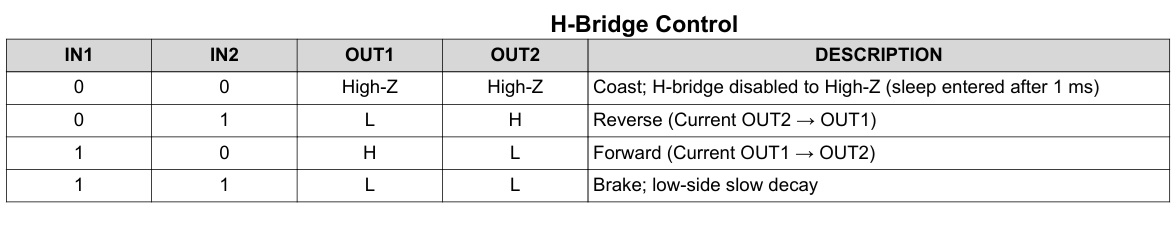
The PWM interface can be used to drive single-coil relays, Dual coil relay, solenoids and DC brushed motor. To actuate a load the driver must supply current in either the forward or reverse state as defined in the PWM control table.
After actuation, the outputs can be disabled (IN1 = IN2 = 0) to place the driver in sleep mode and reduce power consumption. Alternatively, the outputs can be briefly set to brake mode after actuation to suppress back-EMF effects from the relay and prevent current from flowing back into the VM supply node.
When using the DRV8231 device, an external current-sense resistor is required; a 0.22 Ω, 2 W, 1% SMD 2512 resistor is recommended.
Power Supply
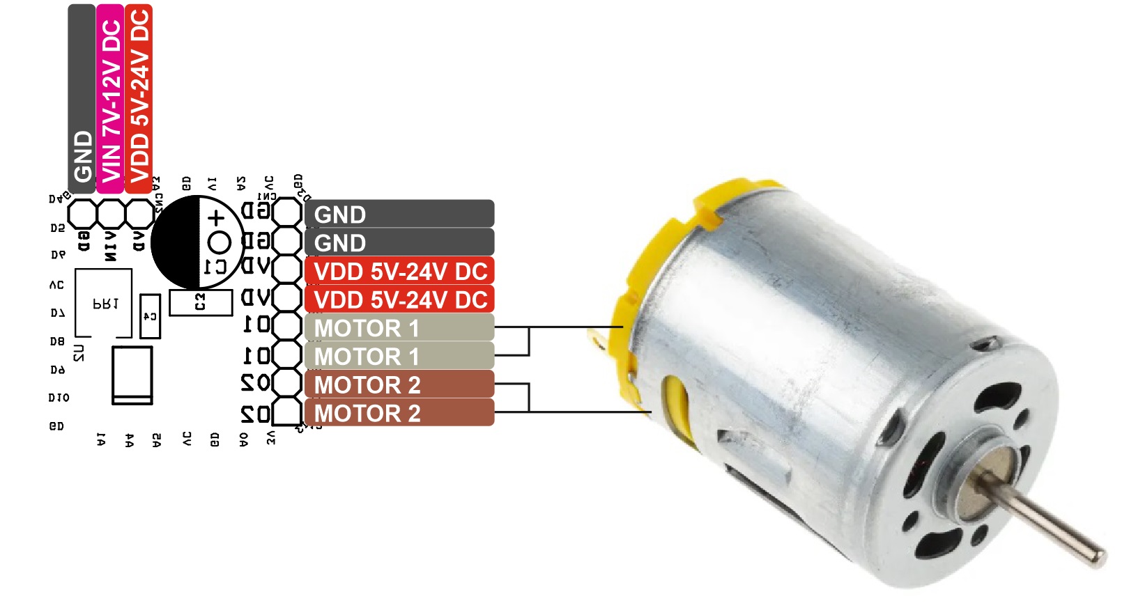
The project requires two power supplies: one for the motor (5 V to 24 V DC) and another for the OLEDUINO-V2 (7 V to 12 V DC). The project can also operate with a single power supply when using a 12 V motor. In this case, install a jumper/shunt between VD and VIN (CN2, Pin 1 and Pin 2). Feed 12V to CN1 Pin 1,2.
Arduino Code
Arduino code (CODE_DRV8231A.zip) is provided to test the shield. Upload the code to the OLEDUINO-V2 and install the shield on the back of the OLEDUINO-V2. Using this code, the motor speed and direction are displayed.
Features
- Load Power Supply 5V to 24V DC (Maximum 33V)
- High output current capability: 3.7-A Peak
- PWM control interface
- Supports 1.8-V, 3.3-V, and 5-V logic inputs
- Integrated IPROPI current sensing for stall detection and current regulation
- Low-power sleep mode
- PCB Dimensions 25.4 x 25.4 mm
The DRV8231A output stage consists of four N-channel MOSFETs designed to drive high current loads. These outputs are controlled by two logic inputs, IN1 and IN2, which are connected to pins D9 and D10 of the Arduino-compatible OLEDUINO-V2 microcontroller.
The inputs can be driven with static logic levels to provide a 100% duty-cycle output, or they can be pulse-width modulated (PWM) to achieve variable motor speed control. When using PWM, switching between drive and brake modes typically provides the best performance.
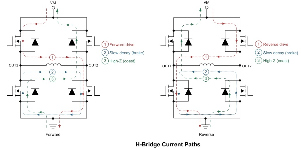
For example, to drive a motor forward at 50% of its maximum RPM, set IN1 = 1 and IN2 = 0 during the drive phase, and IN1 = 1 and IN2 = 1 during the braking phase. Alternatively, the coast mode (IN1 = 0, IN2 = 0) is available for fast current decay.
The schematic illustrates the motor current flow through the H-bridge. The input pins may be powered before the motor supply voltage (VM) is applied.
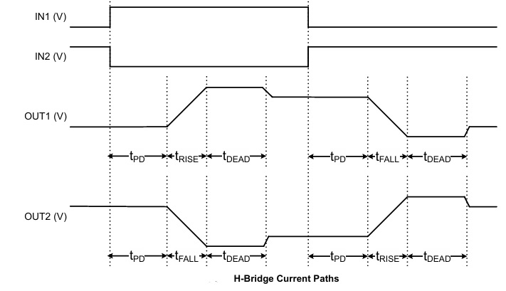
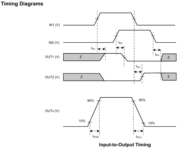
When an output changes from driving high to driving low, or driving low to driving high, dead time is automatically inserted to prevent shoot-through. The tDEAD time is the time in the middle when the output is High-Z. If the output pin is measured during tDEAD, the voltage depends on the direction of current. If the current is leaving the pin, the voltage is a diode drop below ground. If the current is entering the pin, the voltage is a diode drop above VM. This diode is the body diode of the high-side or low-side FET. 1 22 Reverse drive Slow decay (brake) VM 3 3 1 2 Forward drive Slow decay (brake) VM The propagation delay time (tPD) is measured as the time between an input edge to output change. This time accounts for input deglitch time and other internal logic propagation delays. The input deglitch time prevents noise on the input pins from affecting the output state. Additional output slew delay timing accounts for FET turn on or turn off times (tRISE and tFALL).
Current Sense and Regulation (IPROPI)
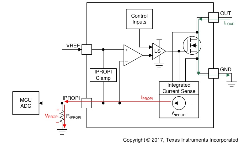
The DRV8231A device integrates current sensing, regulation, and feedback as part of the IPROPI feature. These features allow the device to sense the output current without an external sense resistor or sense circuitry reducing system size, cost, and complexity. This also allows for the device to limit the output current in the case of motor stall or high torque events and give detailed feedback to the controller about the load current through a current proportional output.
Current Sensing
The IPROPI pin outputs an analog current proportional to the current flowing through the low-side power MOSFETs in the H-bridge scaled by AIPROPI. The IPROPI output current can be calculated by Equation 1. The ILSx in Equation 1 is only valid when the current flows from drain to source in the low-side MOSFET. If current flows from source to drain or through the body diode, the value of ILSx for that channel is zero. For instance, if the bridge is in the brake, slow-decay state, then the current out of IPROPI is only proportional to the current in one of the low-side MOSFETs.
IPROPI (μA) = (ILS1 + ILS2) (A) x AIPROPI (μA/A)
The AERR parameter in the Electrical Characteristics table is the error associated with the AIPROPI gain. It indicates the combined effect of offset error added to the IOUT current and gain error. The motor current is measured by an internal current mirror architecture on the low-side FETs which removes the need for an external power sense resistor. The current mirror architecture allows for the motor winding current to be sensed in both the drive and brake low-side slow-decay periods allowing for continuous current monitoring in typical bidirectional brushed DC motor applications. In coast mode, the current is freewheeling and cannot be sensed because it flows from source to drain. However, the current can be sampled by briefly reenabling the driver in either drive or slow-decay modes and measuring the current before switching back to coast mode again.
The IPROPI pin should be connected to an external resistor (RIPROPI) to ground in order to generate a proportional voltage (VIPROPI) on the IPROPI pin with the IIPROPI analog current output. This allows for the load current to be measured as the voltage drop across the RIPROPI resistor with a standard analog to digital converter (ADC). The RIPROPI resistor can be sized based on the expected load current in the application so that the full range of the controller ADC is utilized. Additionally, the DRV8231A device implements an internal IPROPI voltage clamp circuit to limit VIPROPI with respect to VVREF on the VREF pin and protect the external ADC in case of output overcurrent or unexpected high current events. The corresponding IPROPI voltage to the output current can be calculated by Equation 2. VIPROPI (V) = IPROPI (A) x RIPROPI (Ω) (2) The IPROPI output bandwidth is limited by the sense delay time (tDELAY) of the internal current sensing circuit. This time is the delay from the low-side MOSFET enable command (from the INx pins) to the IPROPI output being ready. If the device is alternating between drive and slow-decay (brake) in an H-bridge PWM pattern then the low-side MOSFET sensing the current is continuously on and the sense delay time has no impact to the IPROPI output. If a command on the INx pins disables the low-side MOSFETs (according to the logic tables in Section 8.4.1 data sheet), the IPROPI output will disable with the input logic signal. Although the low-side MOSFETs may still conduct current as they disable according to the device slew rate (noted in the Electrical Characteristics table by tRISE time), IPROPI will not represent the current in the low-side MOSFETs during this turnoff time.
Current Regulatio
The DRV8231A device integrates current regulation using a fixed off-time current chopping scheme. This allows the devices to limit the output current in case of motor stall, high torque, or other high current load events without involvement from the external controller
The current chopping threshold (ITRIP) is set through a combination of the VREF voltage (VVREF) and IPROPI output resistor (RIPROPI). This is done by comparing the voltage drop across the external RIPROPI resistor to VVREF with an internal comparator.
ITRIP (A) x AIPROPI (μA/A) = VVREF (V) / RIPROPI (Ω) (3)
For example, if VVREF = 3.3 V, RIPROPI = 1375 Ω, and AIPROPI = 1500 μA/A, then ITRIP will be approximately 1.6 A.
The fixed off-time current chopping scheme supports up to 100% duty cycle current regulation since the H-bridge automatically enables after the tOFF period and does not require a new control input edge on the INx pins to reset the outputs. When the motor current exceeds the ITRIP threshold, the outputs will enter a current chopping mode with a fixed off time (tOFF). During tOFF, the H-bridge enters a brake/low-side slow decay state (both low-side MOSFETs ON) for tOFF duration after IOUT exceeds ITRIP. After tOFF, the outputs re-enable according to the control inputs if IOUT is less than ITRIP. If IOUT is still greater than ITRIP, the H-bridge enters another period of brake/low-side slow decay for tOFF. If the state of the INx control pins changes during the tOFF time, the remainder of the tOFF time is ignored, and the outputs will again follow the inputs. The ITRIP comparator has both a blanking time (tBLK) and a deglitch time (tDEG). The internal blanking time helps to prevent voltage and current transients during output switching from effecting the current regulation. These transients may be caused by a capacitor inside the motor or on the connections to the motor terminals. The internal deglitch time ensures that transient conditions do not prematurely trigger the current regulation. In certain cases where the transient conditions are longer than the deglitch time, placing a 10-nF capacitor on the IPROPI pin, close to the device, will help filter the transients on IPROPI output so current regulation does not prematurely trigger. The capacitor value can be adjusted as needed, however large capacitor values may slow down the response time of the current regulation circuitry. The internal current regulation and current feedback can be disabled by tying IPROPI to GND and setting the VREF pin voltage greater than GND. If current feedback is required and current regulation is not required, set VVREF and RIPROPI such that VIPROPI never reaches the VVREF threshold. For proper operation of the current regulation circuit, VVREF must be within the range of the VREF pin voltages specified in the Recommended Operating Conditions table.
Overcurrent Protection (OCP)
An analog current limit circuit on each FET limits the current through the FET by limiting the gate drive internally. If this analog current limit persists for longer than the OCP deglitch time (tOCP), all FETs in the H-bridge will disable. The driver re-enables after the OCP retry period (tRETRY) has passed. If the fault condition is still present. Overcurrent conditions are detected independently on both high- and low-side FETs. This means that a short to ground, supply, or across the motor winding will all result in an overcurrent shutdown. Overcurrent protection does not use the current sense circuitry used for current regulation, so it functions regardless of VREF and IPROPI settings.
Thermal Shutdown (TSD)
If the die temperature exceeds safe limits, all FETs in the H-bridge are disabled. After the die temperature has fallen to a safe level, operation automatically resumes.
VM Undervoltage Lockout (UVLO)
Whenever the voltage on the VM pin falls below the UVLO falling threshold voltage, VUVLO, all circuitry in the device is disabled, the output FETS are disabled, and all internal logic is reset. Operation continues when the VVM voltage rises above the UVLO rising threshold
Active Mode
Any fault condition met Disabled See Table 8-4 After the supply voltage on the VM pin has crossed the undervoltage threshold VUVLO, the INx pins are in a state other than IN1 = 0 & IN2 = 0, and tWAKE has elapsed, the device enters active mode. In this mode, the H-bridge, charge pump, and internal logic are active and the device is ready to receive inputs.
Low-Power Sleep Mode
When the IN1 and IN2 pins are both low for time tSLEEP, the DRV8231A device enters a low-power sleep mode. In sleep mode, the outputs remain High-Z and the device draws minimal current from the supply pin (IVMQ). If the device is powered up while all inputs are low, it immediately enters sleep mode. After any of the input pins are set high for longer than the duration of tWAKE, the device becomes fully operational.
Fault Mode Sleep
The DRV8231A device enters a fault mode when a fault is encountered. This is utilized to protect the device and the output load. The device will leave the fault mode and re-enter the active mode when the recovery condition is met.
Stall Detection
Some applications require stall detection to notify the microcontroller of a locked rotor condition. A stall could be caused by one of two things: unintended mechanical blockage or the load reaching an end-stop in a constrained travel path. By using the IPROPI analog current sense feedback of the DRV8231A, the system can implement a simple stall detection scheme. The principle of this stall detection scheme relies on the fact that motor current increases during stall conditions. To implement stall detection, the microcontroller reads the voltage on the IPROPI pin using an ADC and compares it to a stall threshold set in firmware. Alternatively, a comparator peripheral may be used to set this threshold as well.
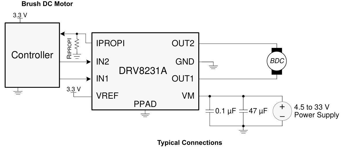
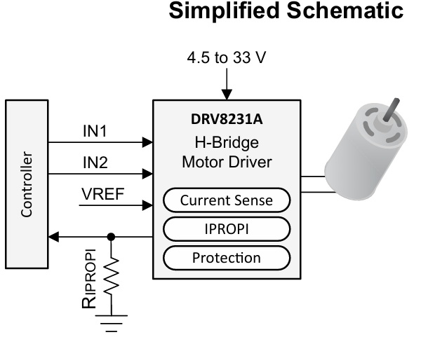
The DRV8231A device is an integrated motor driver with N-channel H-bridge, charge pump, current sense feedback, current regulation, and protection circuitry. The charge pump improves efficiency by supporting N-channel MOSFET half bridges and 100% duty cycle driving.
An internal current mirror architecture on the IPROPI pin implements current sensing and regulation. This eliminates the need for a large power shunt resistor, saving board area and reducing system cost. The IPROPI current-sense output allows a microcontroller to detect motor stall or changes in load conditions. The external voltage reference pin, VREF, determines the threshold of current regulation during start-up and stall events without interaction from a microcontroller.
A low-power sleep mode achieves ultra-low quiescent current draw by shutting down most of the internal circuitry. Internal protection features include supply undervoltage lockout, output overcurrent, and device overtemperature.
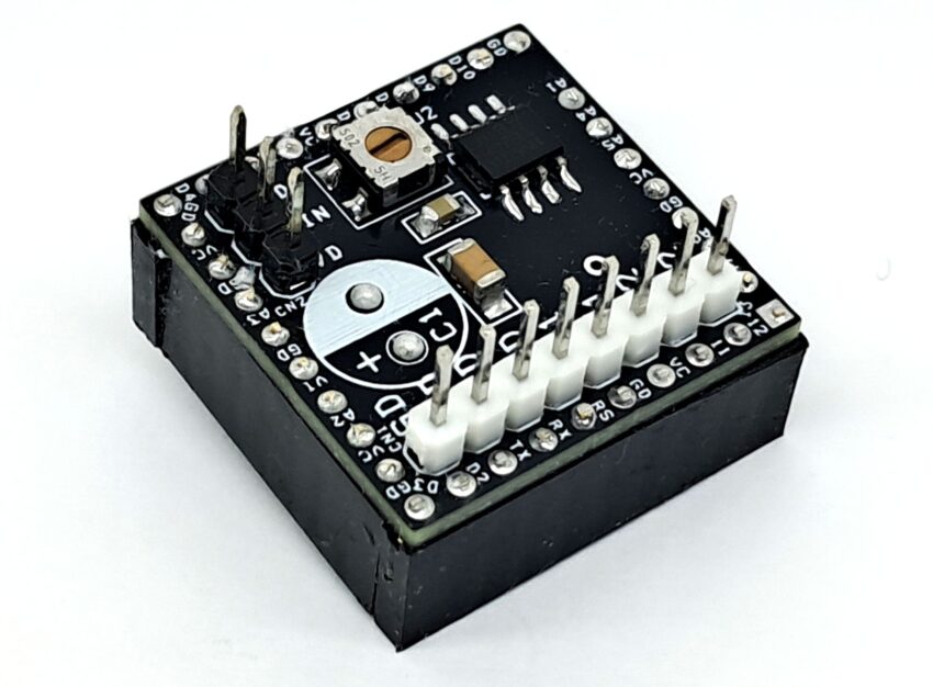
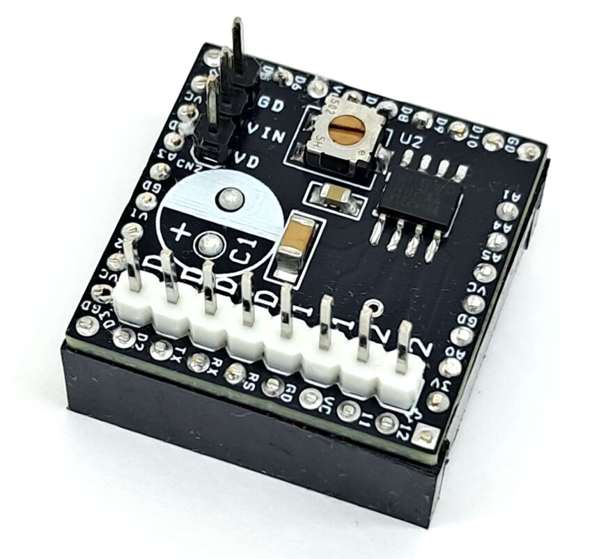
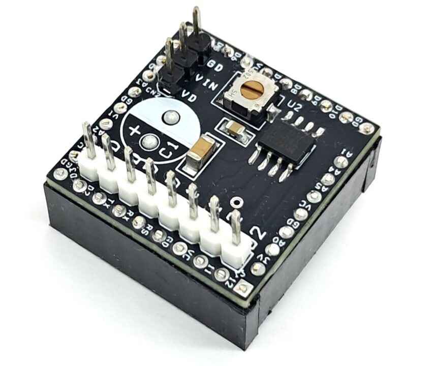
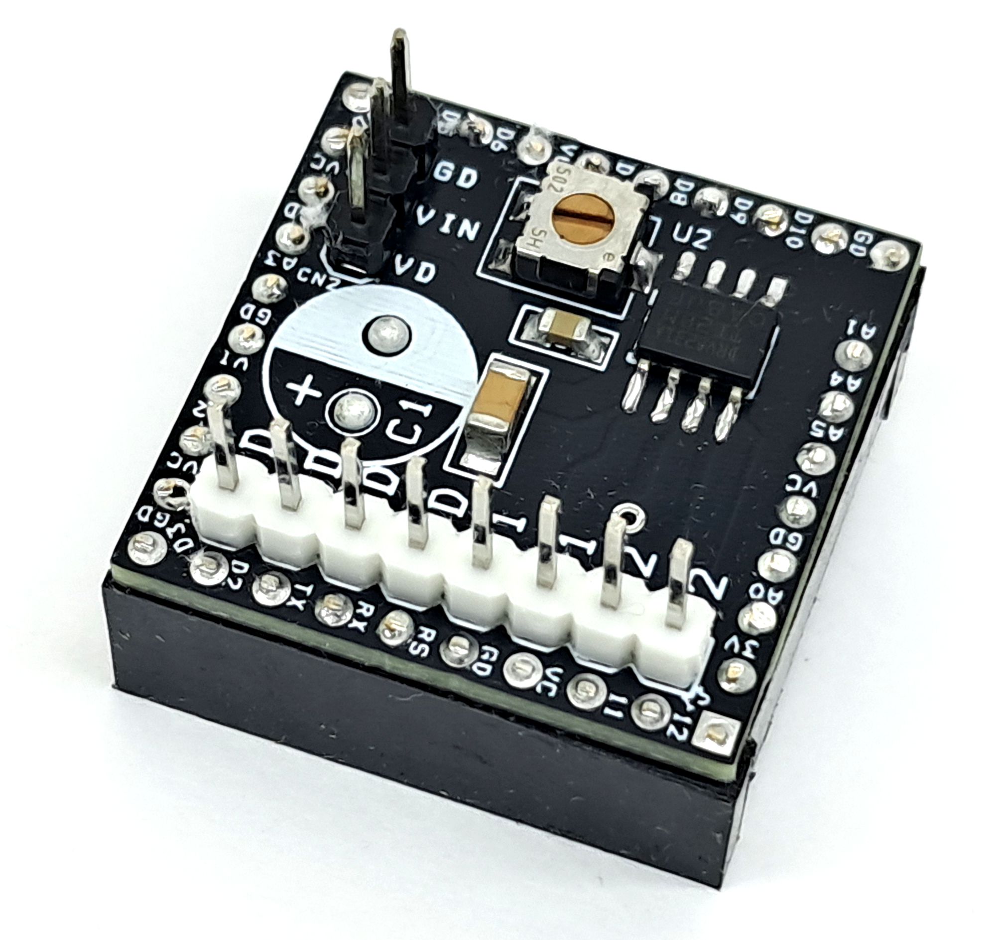
Connections
- CN1: Pin 1,2 = Motor/Output2, Pin 3,4 = Motor/Output1, Pin 5,6 = VDD 5V to 24V DC, Pin 7,8 = GND
- CN2: Pin 1 = VDD 5V-24V DC, Pin 2 = 7V to 12V to OLEDUINO, Pin 3 = GND
- PR1: Current Limit Adjust
Schematic
Parts List
| NO. | QNTY. | REF. | DESC. | MANUFACTURER | SUPPLIER | SUPPLIER PART NO |
|---|---|---|---|---|---|---|
| 1 | 1 | CN1 | 8 PIN MALE HEADER PITCH 2.54MM | WURTH | DIGIKEY | 732-5321-ND |
| 2 | 1 | CN2 | 3 PIN MALE HEADER PITCH 2.54MM | WURTH | DIGIKEY | 732-5316-ND |
| 3 | 1 | C1 | 100uF/35V ELECTROLYTIC 8MM DIA. | PANASONIC | DIGIKEY | P10294-ND |
| 4 | 1 | C3 | 10uF/50V CERAMIC SMD SIZE 0805 | YAGEO/MURATA | DIGIKEY | |
| 5 | 1 | C2 | 0.1uF/50V CERAMIC SMD SIZE 1206 | YAGEO/MURATA | DIGIKEY | |
| 6 | 1 | PR1 | 5K 5MMX4.5MM | NIDEC | DIGIKEY | 563-ST-4ETA502CT-ND |
| 7 | 1 | R1 | 0E SMD SIZE 2512 | YAGEO/MURATA | DIGIKEY | |
| 8 | 2 | U1 | 8 PIN FEMALE HEADER PITCH 2.54MM | WURTH | DIGIKEY | 732-61300811821-ND |
| 9 | 1 | U2 | DRV8231A | TI | DIGIKEY | 296-DRV8231ADDARCT-ND |
| 10 | 1 | C4 | 0.1uF/50V CERAMIC SMD SIZE 0805 | YAGEO/MURATA | DIGIKEY | |
| 11 | 2 | U1 | 10 PIN FEMALE HEADER PITCH 2.54MM | WURTH | DIGIKEY | 732-2859-ND |
Connections
DC Motor Control Diagram
Simplified Schematic Diagram
 H-Bridge Current Path
Single Coil Relay Driving
Dual Coil Relay Driving
Functional Block Diagram

Intergrated Current Path
H-Bridge Current Diagram
Timing Diagram
H-Bridge Logic Truth Table
Gerber View
Photos