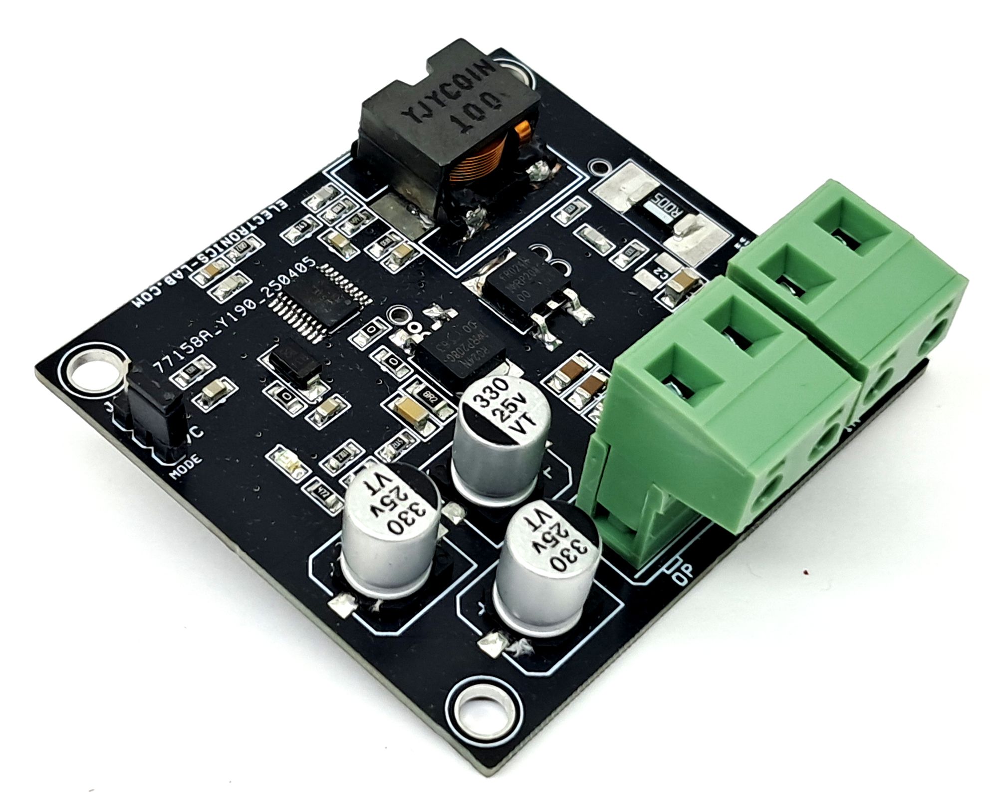
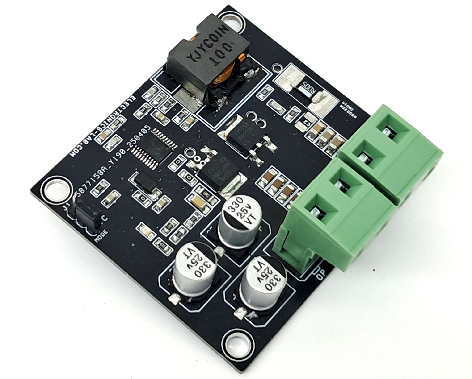
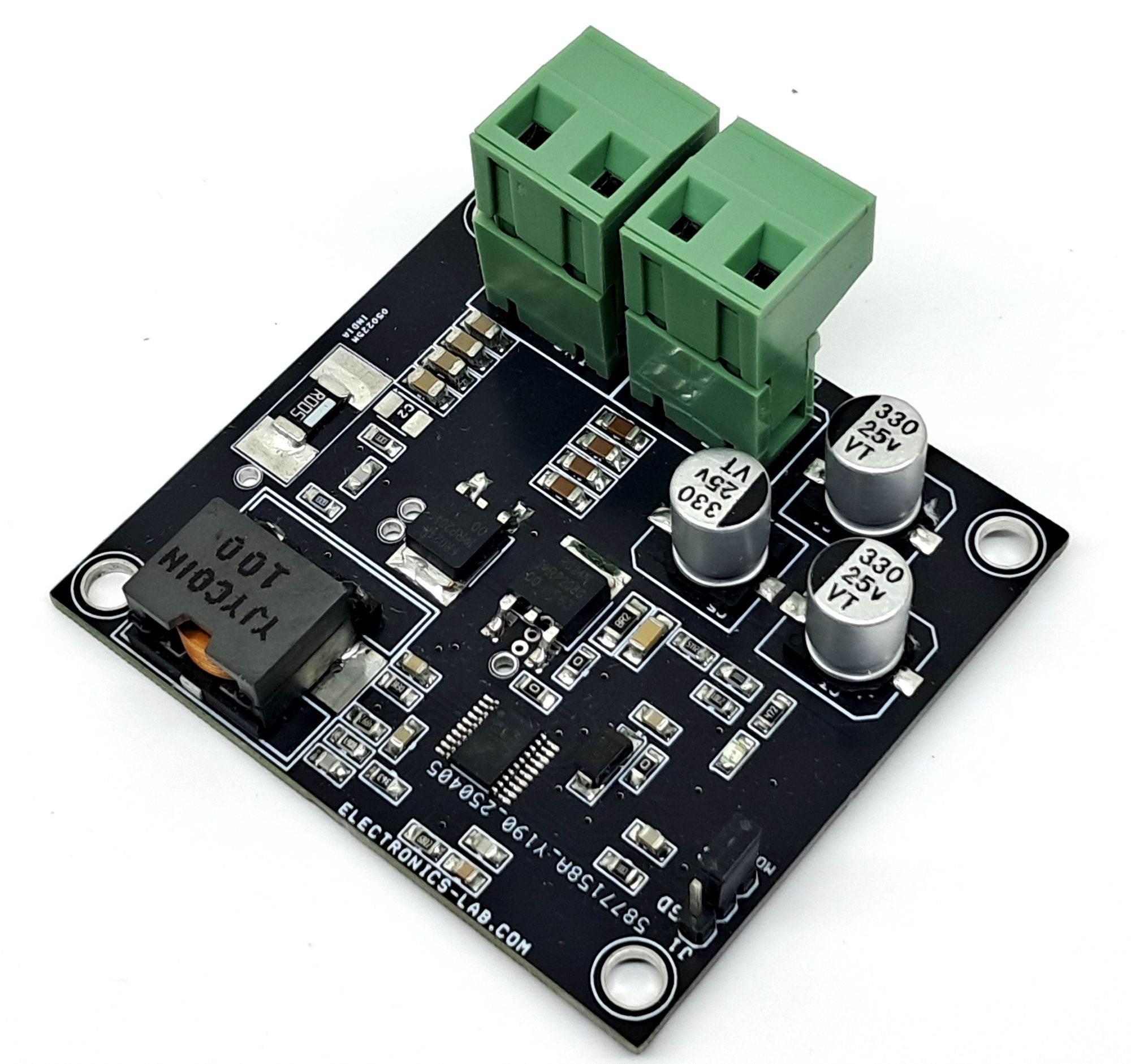
Synchronous Boost Converter 12V Input to 24V Output @ 2A
This project is a synchronous boost converter based on the LM5122 IC. It converts a 12V input to a 24V output capable of delivering up to 2A. It features high-current connectors and a power indicator LED.
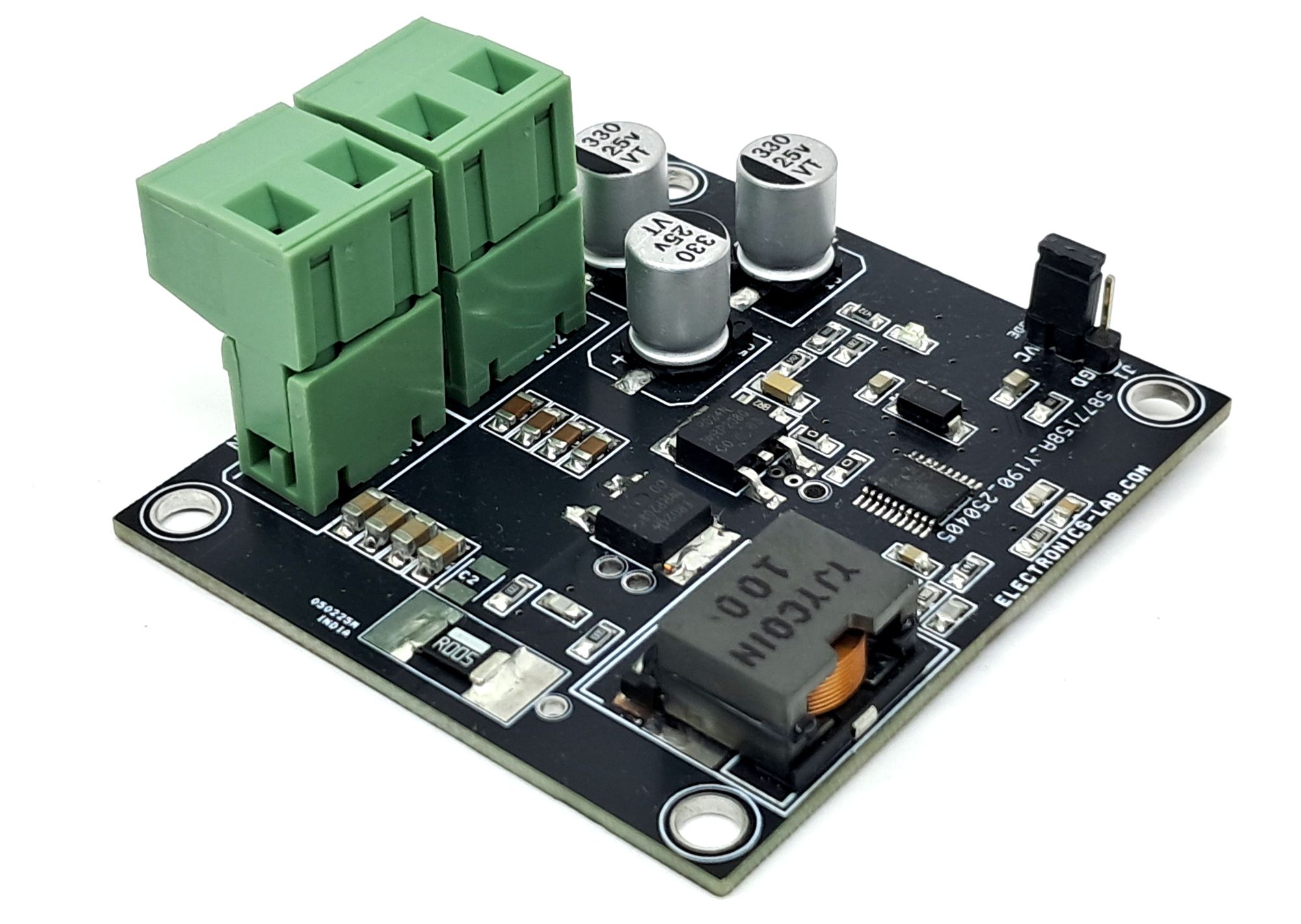
This is a fully functional synchronous boost converter based on the LM5122 controller IC. The project delivers a 24V output at up to 2A from a 12V input. High-current terminal connectors are provided to handle large currents, and an onboard power indicator LED shows the output status.
Features
- Input Supply 12V DC
- Output 24V DC
- Load Current up to 2A
- Switching Frequency 250Khz
- Cycle-by-Cycle Current Limit
- Programmable Line UVLO
- Soft Start
- Thermal Shutdown Protection
- 4 x 4MM Mounting Holes
- PCB Dimensions 62.23 x 56.20 mm
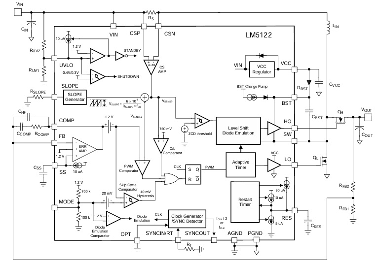
The LM5122 is a multi-phase capable synchronous boost controller intended for high-efficiency synchronous boost regulator applications. The control method is based upon peak-current-mode control. Current-mode control provides inherent line feed forward, cycle-by-cycle current limiting, and ease of loop compensation.
The switching frequency is programmable up to 1 MHz Higher efficiency is achieved by two robust N-channel MOSFET gate drivers with adaptive dead-time control. A user-selectable diode-emulation mode also enables discontinuous-mode operation for improved efficiency at light load conditions.
An internal charge pump allows 100% duty cycle for high-side synchronous switch (bypass operation). A 180° phase shifted clock output enables easy multi-phase interleaved configuration. Additional features include thermal shutdown, frequency synchronization, hiccup-mode current limit, and adjustable line undervoltage lockout.
Thermal Protection
Internal thermal shutdown circuitry is provided to protect the controller in the event the maximum junction temperature is exceeded. When activated, typically at 165°C, the controller is forced into a low-power shutdown mode, disabling the output drivers, disconnection switch and the VCC regulator. This feature is designed to prevent overheating and destroying the device.
MODE Control (Forced-PWM Mode and Diode-Emulation Mode) Jumper J1
A fully synchronous boost regulator implemented with a high-side switch rather than a diode has the capability to sink current from the output in certain conditions such as light load, overvoltage or load transient. The LM5122 can be configured to operate in either forced-PWM mode (FPWM) or diode emulation mode. In FPWM, reverse current flow in high-side N-channel MOSFET switch is allowed, and the inductor current conducts continuously at light or no-load conditions. The benefit of the forced PWM mode is fast light load to heavy load transient response and constant frequency operation at light or no-load conditions. To enable FPWM, connect the MODE pin to VCC or tie to a voltage greater than 1.2 V. In FPWM, reverse current flow is not limited. In diode-emulation mode, current flow in the high-side switch is only permitted in one direction (source to drain). Turn on of the high-side switch is allowed if CSP to CSN voltage is greater than 7 mV rising threshold of zero current detection during low-side switch on-time. If CSP to CSN voltage is less than 6-mV falling threshold of zero current detection during high-side switch on-time, reverse current flow from output to input through the high side N-channel MOSFET switch is prevented and discontinuous conduction mode of operation is enabled by latching off the high-side N-channel MOSFET switch for the remainder of the PWM cycle. A benefit of the diode emulation is lower power loss at light load conditions. During start-up the LM5122 forces diode emulation, for start-up into a pre-biased load, while the SS pin voltage is less than 1.2 V. Forced diode emulation is terminated by a pulse from PWM comparator when SS is greater than 1.2 V. If there are no LO pulses during the soft-start period, a 350-ns one-shot LO pulse is forced at the end of soft start to help charge the boot strap capacitor. Due to the internal current sense delay, configuring the LM5122 for diode emulation mode must be carefully evaluated if the inductor current ripple ratio is high and when operating at very high switching frequency. The transient performance during full load to no load in FPWM mode should also be verified.
MODE Control (Skip-Cycle Mode and Pulse-Skipping Mode)
Light load efficiency of the regulator typically drops as the losses associated with switching and bias currents of the converter become a significant percentage of the total power delivered to the load. In order to increase the light load efficiency, the LM5122 provides two types of light load operation in diode-emulation mode. The skip-cycle mode integrated into the LM5122 controller reduces switching losses and improves efficiency at light-load condition by reducing the average switching frequency. Skip-cycle operation is achieved by the skip cycle comparator. When a light-load condition occurs, the COMP pin voltage naturally decreases, reducing the peak current delivered by the regulator. During COMP voltage falling, the skip-cycle threshold is defined as VMODE–20 mV and during COMP voltage rising, it is defined as VMODE +20 mV. There is 40mV of internal hysteresis in the skip cycle comparator. When the voltage at PWM comparator input falls below VMODE–20 mV, both HO and LO outputs are disabled. The controller continues to skip switching cycles until the voltage at PWM comparator input increases to VMODE + 20 mV, demanding more inductor current. The number of cycles skipped depends upon the load and the response time of the frequency compensation network. The internal hysteresis of skip-cycle comparator helps to produce a long skip cycle interval followed by a short burst of pulses. An internal 700-kΩ pullup and 100-kΩ pulldown resistor sets the MODE pin to 0.15 V as a default. Because the peak current limit threshold is set to 750 mV, the default skip threshold corresponds to approximately 17% of the peak level. In practice the skip level is lower due to the added slope compensation. By adding an external pullup resistor to SLOPE or VCC pin or adding an external pulldown resistor to the ground, the skip cycle threshold can be programmed. Because the skip cycle comparator monitors the PWM comparator input which is proportional to the COMP voltage, skip-cycle operation is not recommended when the bypass operation is required. Conventional pulse-skipping operation can be achieved by connecting the MODE pin to ground. The negative 20-mV offset at the positive input of skip-cycle comparator ensures the skip-cycle comparator does not trigger in normal operation. At light or no-load conditions, the LM5122 skips LO pulses if the pulse width required by the regulator is less than the minimum LO on-time of the device. Pulse skipping appears as a random behaviour as the error amplifier struggles to find an average pulse width for LO in order to maintain regulation at light or no-load conditions.
Hiccup-Mode Overload Protection
If cycle-by-cycle current limit is reached during any cycle, a 30-μA current is sourced into the RES capacitor for the remainder of the clock cycle. If the RES capacitor voltage exceeds the 1.2-V restart threshold, a hiccup mode over load protection sequence is initiated; The SS capacitor is discharged to GND, both LO and HO outputs are disabled, the voltage on the RES capacitor is ramped up and down between 2-V hiccup counter lower threshold and 4-V hiccup counter upper threshold eight times by 10-μA charge and 5-μA discharge currents. After the eighth cycles, the SS capacitor is released and charged by the 10-μA soft-start current again. If a 3-V Zener diode is connected in parallel with the RES capacitor, the regulator enters into the hiccup-mode off mode and then never restarts until UVLO shutdown is cycled. Connect RES pin directly to the AGND when the hiccup mode operation is not used.
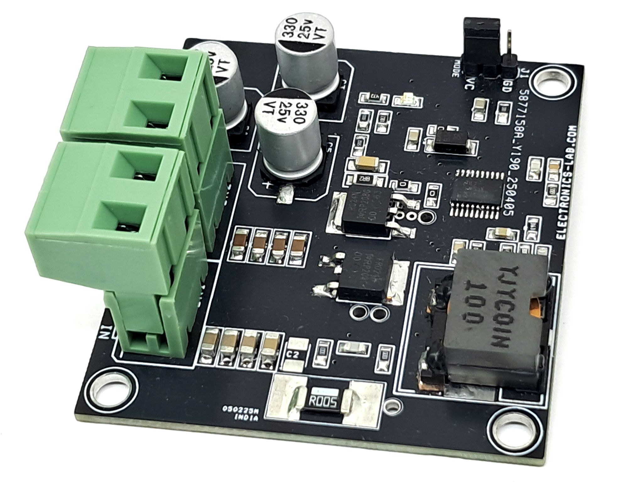
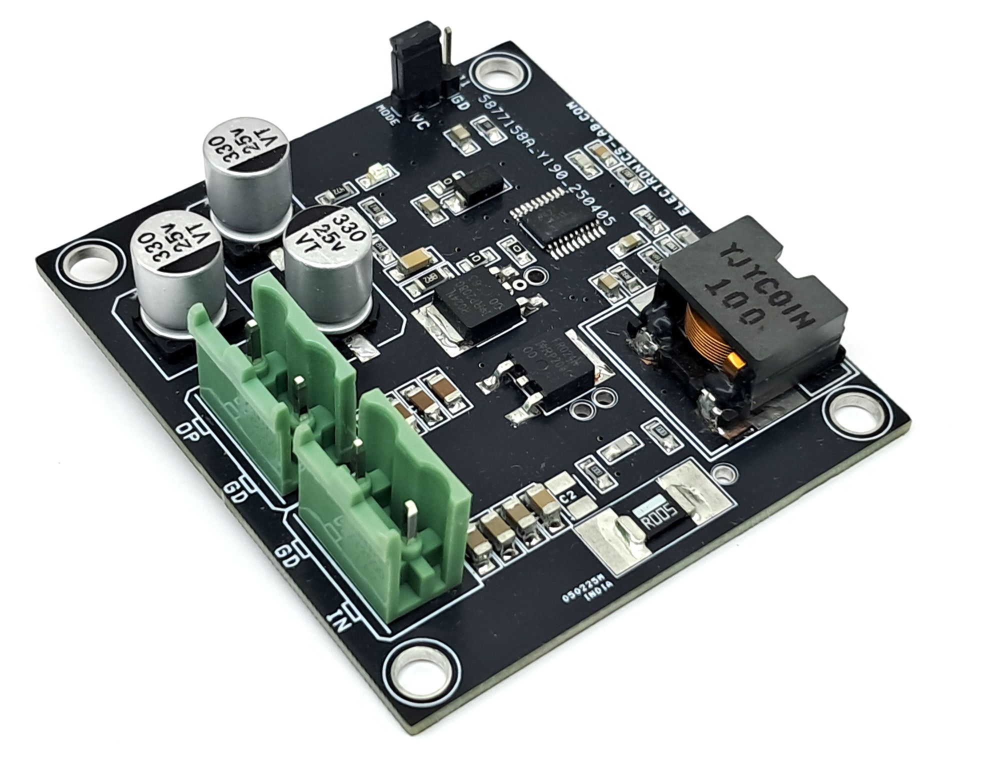
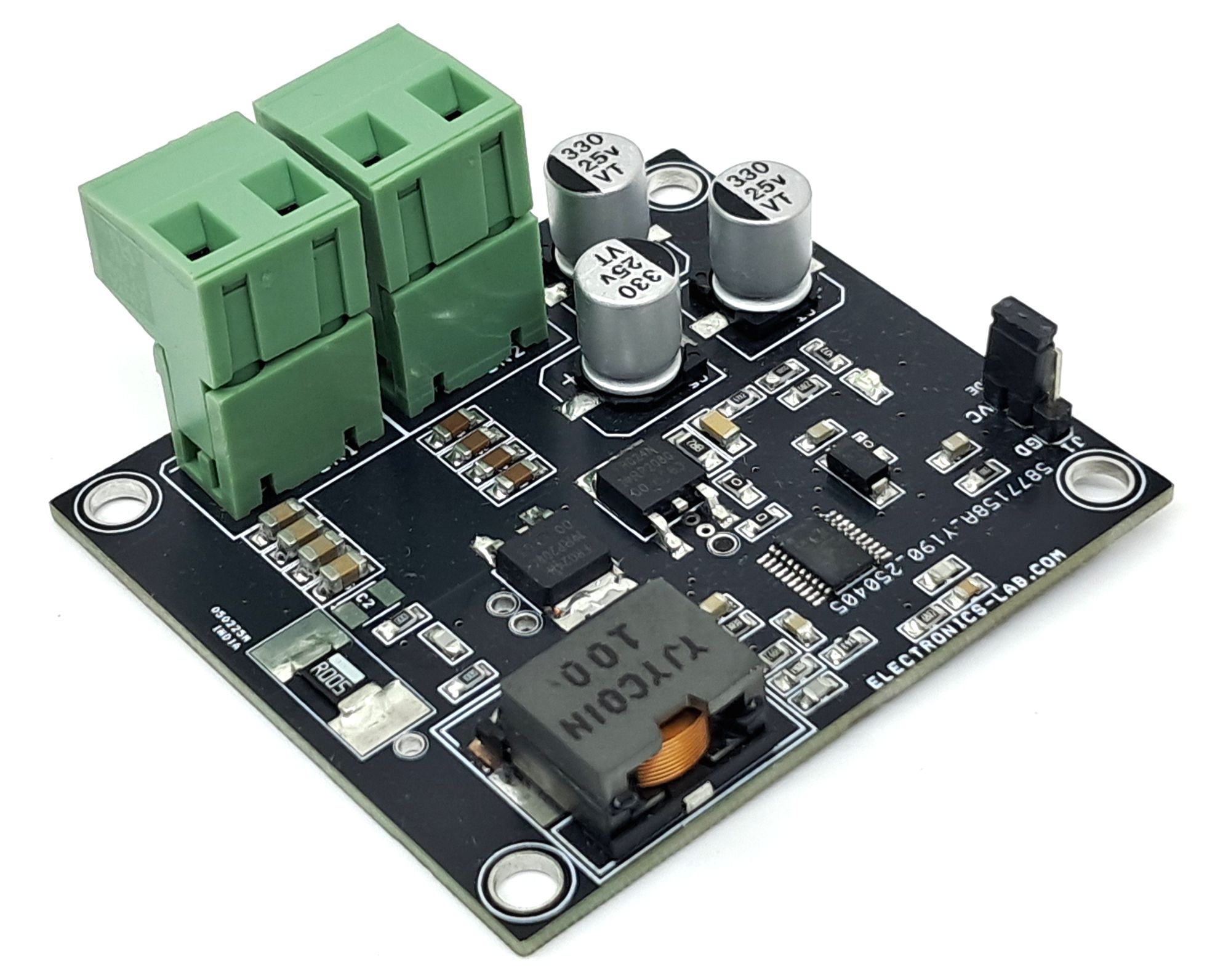
Connections
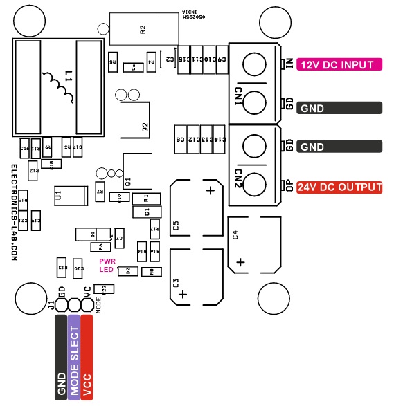
- CN1: Pin 1 = +12V DC Input, Pin 2 = GND
- CN2: Pin 1 = +24V DC Output, Pin 2 = GND
- D2: Power LED
- Jumper J1 Mode Selection: Jumper VCC FPWM, Jumper GND Pulse Skip, Jumper Open Skip Cycle Mode
Schematic
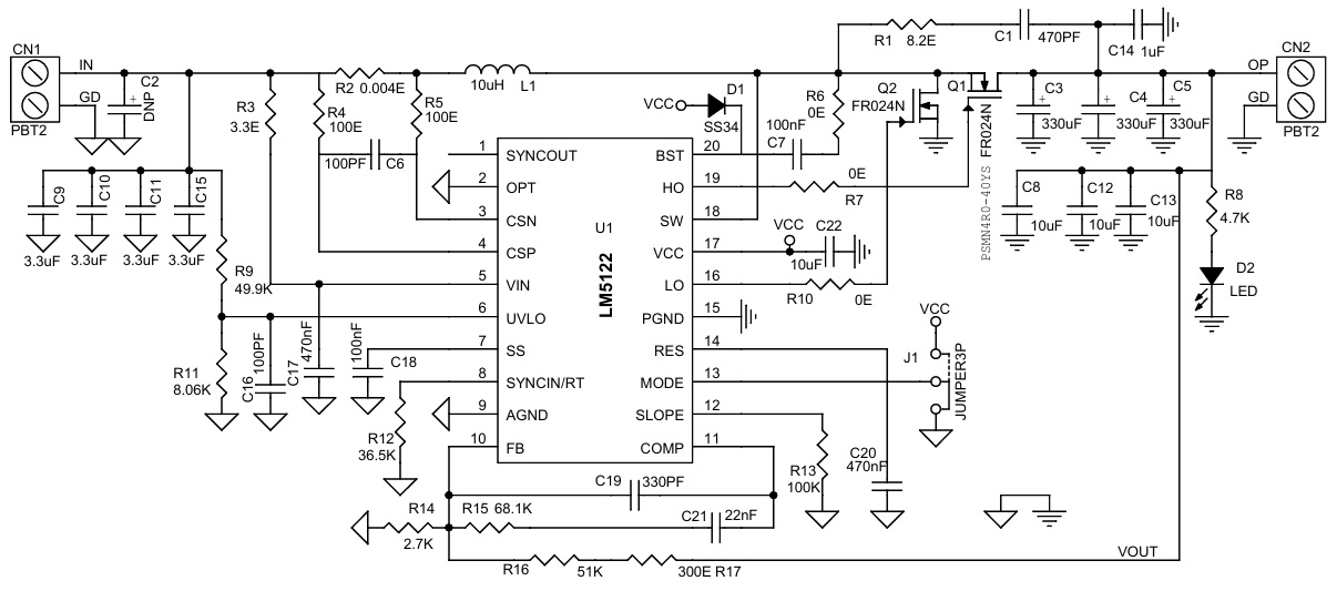
Parts List
| NO | QNTY. | REF | DESC. | MANUFACTURER | SUPPLIER | SUPPLIER PART NO |
|---|---|---|---|---|---|---|
| 1 | 2 | CN1,CN2 | 2 PIN SCREW TERMINAL PITCH 7.62MM | WURTH | DIGIKEY | 732-691254410002-ND |
| 2 | 1 | C1 | 470PF/50V CERAMIC SMD SIZE 1206 | YAGEO/MURATA | DIGIKEY | |
| 3 | 1 | C2 | DNP | |||
| 4 | 3 | C3,C4,C5 | 330uF/35V ELECTROLYTIC | NICHICOM | DIGIKEY | 493-2293-1-ND |
| 5 | 2 | C6,C16 | 100PF/50V CERAMIC SMD SIZE 0805 | YAGEO/MURATA | DIGIKEY | |
| 6 | 2 | C7,C18 | 100nF/50V CERAMIC SMD SIZE 0805 | YAGEO/MURATA | DIGIKEY | |
| 7 | 3 | C8,C12,C13 | 10uF/35V CERAMIC SMD SIZE 1206 | YAGEO/MURATA | DIGIKEY | |
| 8 | 4 | C9,C10,C11,C15 | 3.3uF/35V CERAMIC SMD SIZE 1206 | YAGEO/MURATA | DIGIKEY | |
| 9 | 1 | C14 | 1uF/35V CERAMIC SMD SIZE 1206 | YAGEO/MURATA | DIGIKEY | |
| 10 | 2 | C17,C20 | 470nF/35V CERAMIC SMD SIZE 0805 | YAGEO/MURATA | DIGIKEY | |
| 11 | 1 | C19 | 330PF/35V CERAMIC SMD SIZE 0805 | YAGEO/MURATA | DIGIKEY | |
| 12 | 1 | C21 | 22nF/35V CERAMIC SMD SIZE 0805 | YAGEO/MURATA | DIGIKEY | |
| 13 | 1 | D1 | SS34 SMD | MDD | DIGIKEY | 3372-SS34TR-ND |
| 14 | 1 | D2 | LED RED SMD SIZE 0805 | OSRAM | DIGIKEY | 475-1278-1-ND |
| 15 | 1 | J1 | 3 PIN MALE HEADER PITCH 2.54MM | WURTH | DIGIKEY | 732-5316-ND |
| 16 | 1 | L1 | 10uH/15A 18x18MM | WURTH | DIGIKEY | 732-2167-1-ND |
| 17 | 2 | Q1,Q2 | FR024N DPAK | VISHAY | DIGIKEY | IRFR024-ND |
| 18 | 1 | R1 | 8.2E 5% SMD SIZE 1206 | YAGEO/MURATA | DIGIKEY | |
| 19 | 1 | R2 | 0.004E/3W 1% SMD SIZE 2512 | BOURNS INC | DIGIKEY | CRE2512-FZ-R004E-3CT-ND |
| 20 | 1 | R3 | 3.3E 5% SMD SIZE 0805 | YAGEO/MURATA | DIGIKEY | |
| 21 | 2 | R4,R5 | 100E 5% SMD SIZE 0805 | YAGEO/MURATA | DIGIKEY | |
| 22 | 3 | R6,R7,R10 | 0E SMD SIZE 0805 | YAGEO/MURATA | DIGIKEY | |
| 23 | 1 | R8 | 4.7K 5% SMD SIZE 0805 | YAGEO/MURATA | DIGIKEY | |
| 24 | 1 | R9 | 49.9K 1% SMD SIZE 0805 | YAGEO/MURATA | DIGIKEY | |
| 25 | 1 | R11 | 8.06K 1% SMD SIZE 0805 | YAGEO/MURATA | DIGIKEY | |
| 26 | 1 | R12 | 36.5K 1% SMD SIZE 00805 | YAGEO/MURATA | DIGIKEY | |
| 27 | 1 | R13 | 100K 1% SMD SIZE 0805 | YAGEO/MURATA | DIGIKEY | |
| 28 | 1 | R14 | 2.7K 1% SMD SIZE 0805 | YAGEO/MURATA | DIGIKEY | |
| 29 | 1 | R15 | 68.1K 1% SMD SIZE 0805 | YAGEO/MURATA | DIGIKEY | |
| 30 | 1 | R16 | 51K 1% SMD SIZE 0805 | YAGEO/MURATA | DIGIKEY | |
| 31 | 1 | R17 | 300E 5% SMD SIZE 0805 | YAGEO/MURATA | DIGIKEY | |
| 32 | 1 | U1 | LM5122 | TI | DIGIKEY | 296-LM5122ZPWPTCT-ND |
| 33 | 1 | C22 | 10uF/35V CERAMIC SMD SIZE 0805 | YAGEO/MURATA | DIGIKEY | |
| 34 | 1 | SHUNT | SHUNT FOR JUMPER | SULLINS CONECT | DIGIKEY | S9001-ND |
Connections
Block Diagram
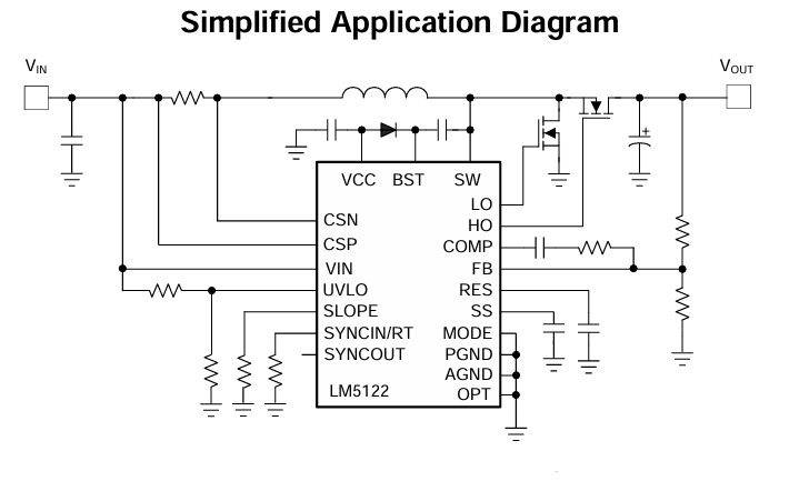
Application Schematic
Gerber View
Photos