Diodes Integrates Sync-Buck Controller With Type-C PD3.1 Source Controller
The APK43070 buck controller targets single-port and multiple-port USB PD charging applications, offering high power efficiency and low standby power in a small footprint.
Designing a USB power delivery (PD) charger typically means pairing a dedicated PD protocol controller with a separate power stage controller: two chips, more board space, and a longer bill of materials. Diodes Incorporated’s new APK43070 takes a different approach by folding both functions into a single device, targeting single- and multiple-port charging applications where board area and component count are ongoing concerns.
Single-Chip Buck Controller With USB PD3.1 Source Controller
The APK43070 is a synchronous buck controller with an integrated USB Type-C PD3.1 source controller. On the power delivery side, it supports a standard power range with a programmable power supply up to 21 V and an extended power range with an adjustable-voltage supply up to 28 V, covering charging power up to 100 W under SPR and up to 140 W under EPR.
Diodes’ new APK43070 comes in a compact 4 mm x 4 mm W-QFN4040-24 package. Image used courtesy of Diodes Incorporated
The buck controller portion is a constant-frequency, synchronous step-down design with integrated drivers for external N-MOSFETs. The switching frequency is configurable to 125 kHz, 250 kHz, 350 kHz, or 400 kHz via a precision resistor on GPIO3. The controller supports duty cycles up to 95% and includes a VIN DC pass-through mode that allows the input rail to feed the output directly when the voltage difference is small enough, reducing unnecessary switching losses.
One practical benefit of combining these two blocks is that, because the buck controller’s high-side and low-side MOSFETs already control the output VBUS, the separate PD output-switch MOSFET normally required per port can be eliminated. In a multi-port system, that’s a meaningful reduction in component count.
Multi-Port Operation Without an External MCU
The APK43070 is built around an I2C interface with a master/slave addressing scheme, allowing up to eight port addresses to share a single bus without requiring a host microcontroller. Each device’s I2C address is set by connecting a 1% precision resistor to the GPIO1 pin, so adding or reconfiguring ports is straightforward.
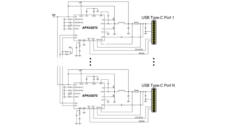
Circuit topology of a multi-port PD3.1 charging application. Image used courtesy of Diodes Incorporated
Power sharing between ports is managed over the I2C bus. An interrupt and wake-up mechanism means slave devices remain in a low-power state until an attach, detach, or fault event occurs, at which point the master is notified to reassign power budgets. This keeps standby consumption low across the full array of ports.
Source PDO power profiles are either selected via a resistor or pre-assigned in firmware, and the chip supports BC1.2, as well as Qualcomm Quick Charge 3.0, 4, 4+, and 5.0, alongside the PD3.1 protocols.
Single-Port and Multiple-Port Charging Applications
The APK43070 includes a full suite of protection functions: overvoltage, undervoltage, overcurrent, and overtemperature, all with auto-recovery. Output current is monitored through a 5 mΩ sense resistor. The device’s high-voltage fabrication process provides VBUS short protection on the CC1, CC2, DP, and DN pins up to 30 V. Moisture detection on the DP/DN pins is also supported, helping flag connector contamination before a fault occurs.
The APK43070 is available in a compact package and is suited for high-power-density chargers, adapters, power strips, and power hubs where space and bill of materials cost are significant design constraints.


