Kyocera Debuts “Ultra-Compact, Ultra-Low Voltage” Clock Oscillator Series
The KC1210A series clock oscillators feature a compact design of 1.25 mm × 1.05 mm × 0.5 mm and a low-voltage operation of 0.9 V, offering reduced power consumption for high-density electronic designs.
Kyocera Corporation has announced the development of the KC1210A series, a new line of clock oscillators designed to address the footprint and power constraints of modern mobile and wearable electronics. The series features a miniaturized form factor and operates at a nominal supply voltage of 0.9 V. These specifications are intended to support the increasing density of components in smartphones, VR headsets, and IoT modules, where board space and battery life are critical design parameters.
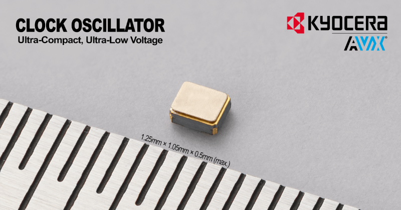
Kyocera’s KC1210A series clock oscillators feature a compact size of just 1.25 mm x 1.05 mm x 0.5 mm. Image used courtesy of Kyocera Corporation
Physical Dimensions and Footprint Reduction
The KC1210A series of clock oscillators is housed in a small package measuring 1.25 mm (length) × 1.05 mm (width) with a maximum height profile of 0.5 mm. According to Kyocera, this design represents a significant reduction in physical volume compared to the company’s previous generation of oscillators. Specifically, the mounting area is approximately 1.31 mm², which, according to Kyocera, is roughly a 60% reduction compared to the earlier KC2016K model (2.0 mm × 1.6 mm).
The volume of the device has been reduced to approximately one-quarter of the KC2016K. This miniaturization is achieved through proprietary element design technology, which enables the crystal element to maintain its performance characteristics despite the reduced physical mass. For engineers designing high-density PCBs, this footprint reduction facilitates tighter component placement, potentially freeing up board space for additional sensors or battery capacity in space-constrained enclosures.
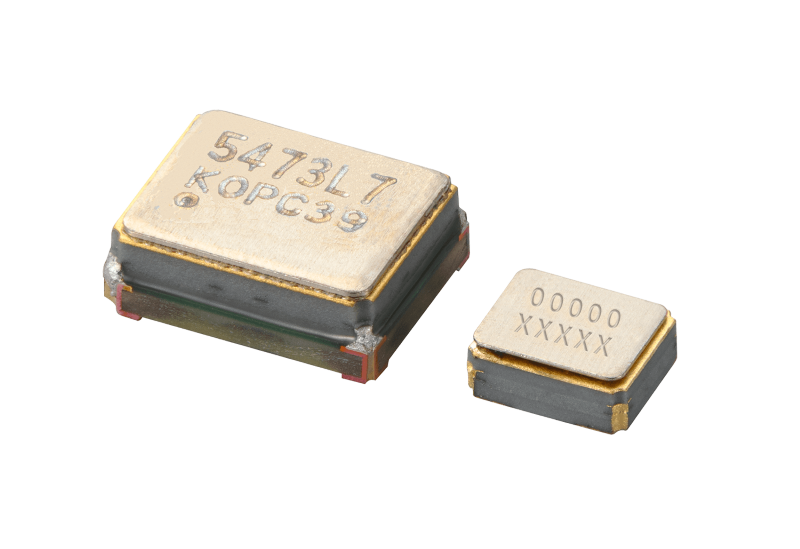
A comparison of Kyocera’s conventional series of clock oscillators, the KC2016K (left), and the newly launched KC1210A (right). Image used courtesy of Kyocera Corporation
Electrical Specifications and Performance
A key technical differentiator for the KC1210A series is its low-voltage operation. The device is specified to operate with a supply voltage ranging from 0.8 V to 1.8 V, with a nominal operating point at 0.9 V. This contrasts with many conventional oscillators that typically require 1.8 V, 2.5 V, or 3.3 V rails. By operating at 0.9 V, the oscillator aligns with the trending lower core voltages of modern low-power microcontrollers and application processors, potentially eliminating the need for level shifters or separate higher-voltage power rails for the clocking subsystem.
Current consumption is specified at a maximum of 3.5 mA when operating at 50 MHz with a 0.9 V supply and a 15 pF load. The output type is CMOS, making it compatible with standard logic families used in embedded systems.

Kyocera has designed the KC1210A series clock oscillators to bring compact energy savings to wearables, IoT devices, and smartphones. Image used courtesy of Adobe Stock
Additionally, the series supports a broad output frequency range from 9.6 MHz to 100 MHz. Frequency tolerance is available in two grades, depending on the operating temperature range: ±25 × 10⁻⁶ (ppm) over the range of -40°C to 85°C and ±50 × 10⁻⁶ (ppm) over the extended range of -40°C to 105°C.
This total frequency tolerance figure includes initial tolerance at 25°C, frequency stability over temperature, supply voltage variation, load capacitance variation, first-year aging at 25°C, and effects from vibration and shock.
Energy-Efficient, High-Density Designs
The release of the KC1210A series serves as a new option for clock generation in ultra-compact designs. By combining a 1.25 mm × 1.05 mm footprint with a 0.9 V operating voltage, the devices directly address the thermal and spatial challenges inherent in next-generation portable electronics. Primary applications include smartphones, virtual reality goggles, smartwatches, and various IoT modules, where minimizing power consumption and PCB area is a priority. The extended temperature range up to 105°C also suggests viability for industrial sensors operating in harsh thermal environments.