Metalenz and STMicroelectronics collaboratively announce the world’s first optical metasurface technology
Metalenz, the fabless semiconductor company, and the Swiss semiconductor manufacturing company STMicroelectronics announced the VL53L8 direct Time-of-Flight (dToF) sensor, a market debut of the meta-optics devices developed through their partnership. The meta-optics technology by Metalenz can replace existing complex and multi-element lenses and provide new functionality.
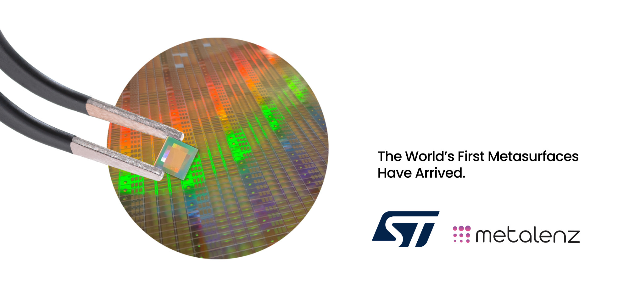
Metalenz, the fabless semiconductor company, and the Swiss semiconductor manufacturing company STMicroelectronics announced the VL53L8 direct Time-of-Flight (dToF) sensor, a market debut of the meta-optics devices developed through their partnership.
The meta-optics technology by Metalenz can replace existing complex and multi-element lenses and provide new functionality. This is achieved by supplying 3D sensor modules that improve performance, power, size, and cost in various consumer, automotive, and industrial applications. The metasurface technology has been made commercially available for the first time now for its use in consumer electronics.
The co-founder and CEO of Metalenz, Rob Devlin, said,
“We have multiple wins that mark the first application of our platform technology, and we are now designing entire systems around its unique functionality. Our meta-optics enable exciting new markets and new sensing capabilities in mobile form factors and at a competitive price.”
The metalens technology by Metalenz is completely planar, unlike traditional curved and molded lenses. The planar metasurface optics are now manufactured on silicon wafers alongside electronics in STMicroelectronics’ front-end semiconductors. While taking up less area, meta-optics collect more light, give several functionalities in a single layer, and enable new forms of sensing in smartphones and other devices. Certain existing optics in ST’s FlightSense ToF modules have been replaced by Metalenz’s flat-lens technology, allowing it to serve in applications like drones, robots, smartphones, and vehicles.
The executive vice president and general manager of ST’s Imaging Sub-Group, Eric Aussedat, said that
“Perfectly complementing ST’s advanced manufacturing capabilities and ToF technology, the introduction of products embedding Metalenz’s game-changing metasurface optics now enables significant power efficiency, optical performance, and module-size optimization that all bring benefit across consumer, industrial, and automotive markets.”
The collaboration between Metalenz IP and ST manufacturing brings together the accuracy and precision of the electronics chip industry to make very precise and repeatable meta-optics. This furthermore unlocks a completely new way to make lenses that combine high quality with large-scale, cost-effective manufacturing.
More information on this revolutionary optical technology can be found on the press release page in the newsroom.


