
Nordic nRF54LC10A – An Ultra-Low-Power Multiprotocol SoC for Cost-Sensitive IoT
This new chip brings Bluetooth Channel Sounding, an Arm Cortex-M33 core, and sub-50 nA hibernation to cost-sensitive trackers and IoT sensors in a tiny 1.9×2.3 mm package.
Nordic Semiconductor has announced the nRF54LC10A, an ultra-low-power multiprotocol SoC designed for space-constrained, cost-sensitive products. The SoC features a 128 MHz Arm Cortex-M33 microcontroller with 1 MB of non-volatile memory (NVM) and 192 KB of RAM. It fully supports Bluetooth Low Energy (LE) with Channel Sounding, as well as IEEE 802.15.4 for Thread, Zigbee, and Matter for simple sensors.
Manufactured on a low-leakage 22nm process node, the nRF54LC10A features sub-50 nA hibernation mode. This is particularly useful for devices like asset trackers and medical tags that ship with batteries already installed, as it ensures shelf current is kept low enough for devices to arrive fully charged after months in storage.
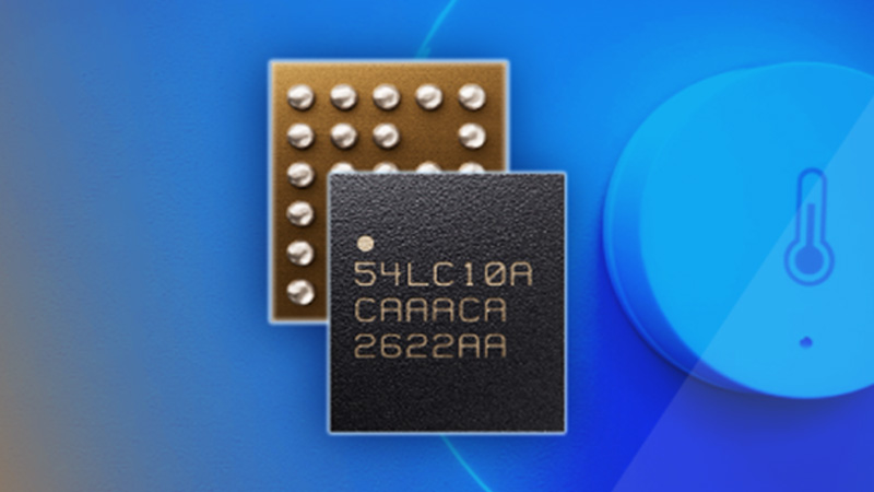
Nordic Semiconductor nRF54LC10A wireless SoC
Nordic nRF54LC10A Key Specifications:
- MCU Core: 128 MHz Arm Cortex-M33 processor with DSP and FPU
- Coprocessor: 128 MHz RISC-V coprocessor for time-critical tasks and SoftPeripherals
- Memory/Storage: 192 KB RAM and 1 MB NVM
- Wireless Connectivity:
- Bluetooth LE with Bluetooth Channel Sounding
- 802.15.4 for Thread, Zigbee, and Matter (simple sensors)
- 2.4 GHz proprietary protocols up to 4 Mbps
- Max TX power: +4 dBm
- Sensitivity: -97 dBm (1 Mbps BLE), -101 dBm (802.15.4)
- Peripherals: 3x SPI/TWI/UART interfaces, ADC (up to 14-bit with oversampling), Global RTC (available in System OFF)
- Security: Arm TrustZone isolation, secure boot, tamper detection, secure storage, and cryptographic engine with side-channel leakage protection
- Power Consumption:
- Radio at 3V: 4.0 mA for RX, 5.8 mA for TX @ 0 dBm
- Sleep mode: 0.5 μA to 1.6 μA (at 3 V)
- Hibernation mode: <50 nA
- Processing efficiency: 239 CoreMark/mA (503 CoreMark total)
- Packages:
- CSP29 (1.93 x 2.29 mm) – 12 GPIOs, 0.35mm pitch
- CSP39 (1.93 x 2.29 mm) – 20 GPIOs, 0.3mm pitch
- QFN48 (6.0 x 6.0 mm) – 31 GPIOs, 0.4mm pitch
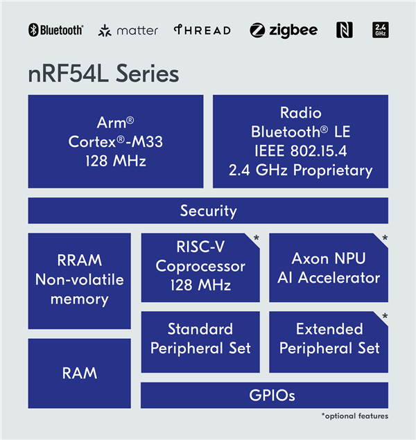
Block diagram of the nRF54L Series architecture and key features
The nRF54LC10A is supported by the nRF Connect SDK and nRF Cloud for device management and remote Firmware-Over-The-Air (FOTA) updates. It also supports Edge AI workloads using Neuton models running on the Cortex-M33 core.
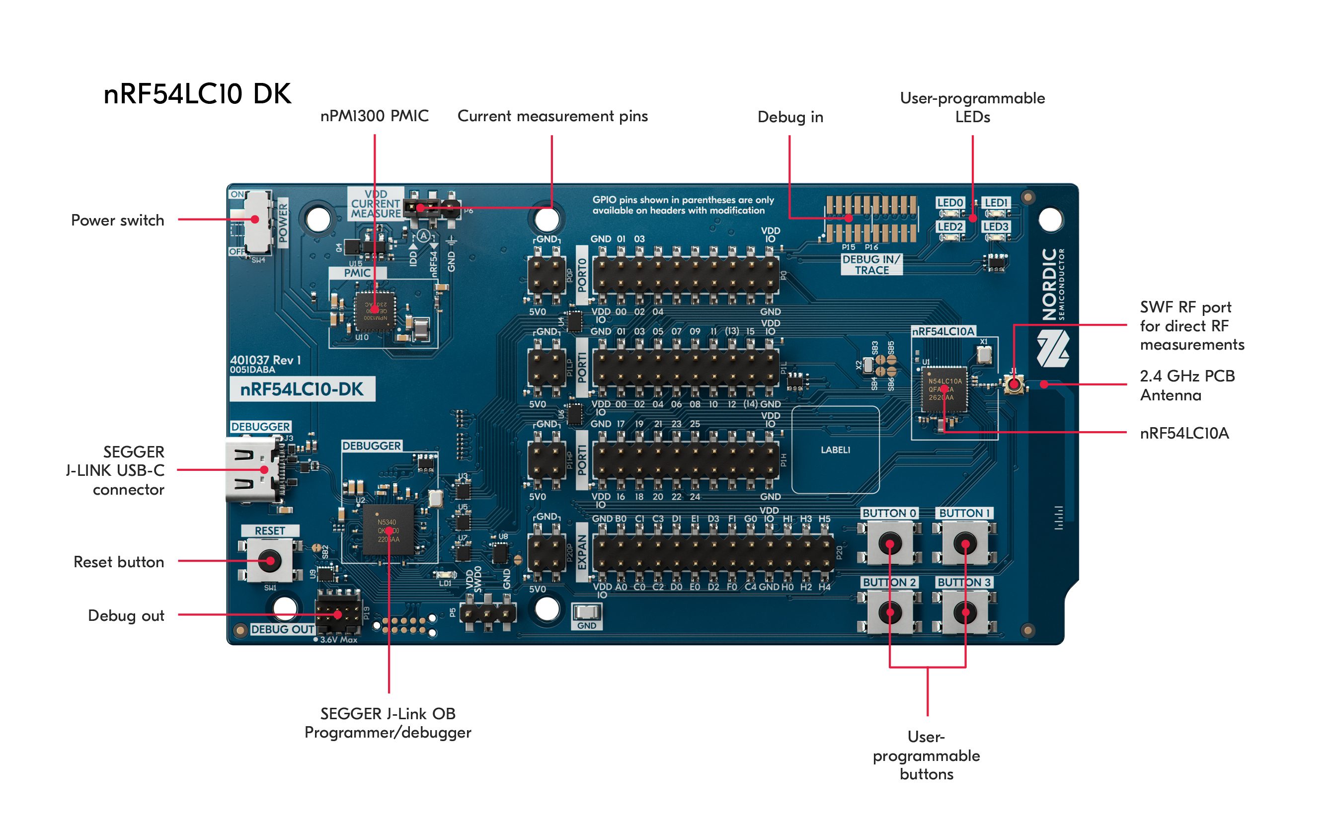
Development kit for the nRF54LC10A with onboard debugger, antenna, buttons, LEDs, and measurement interfaces.
Nordic also offers the nRF54LC10 DK, a development board for developing and testing applications with the nRF54LC10A.
The nRF54LC10A is a lower-memory, lower-peripheral variant of the nRF54L15. While the nRF54L15 offers up to 1.5 MB NVM, 256 KB RAM, and additional peripherals such as NFC, I2S, and PWM, the nRF54LC10A uses 1 MB NVM and 192 KB RAM with a smaller peripheral set while retaining the same multiprotocol wireless support, including Bluetooth LE, Thread, Zigbee, and Matter.
For applications that do not require multiprotocol support or Bluetooth Channel Sounding, Nordic also offers the Bluetooth LE-only nRF54LS05A and nRF54LS05B. Compared with the nRF52 series, Nordic states that the nRF54L series’ 22 nm architecture reduces power consumption by roughly 30–50% in typical Bluetooth LE use cases while providing twice the processing power.
The Nordic nRF54LC10A Ultra-low-power multiprotocol SoC is currently available for early sampling through a project-based early access program. The nRF54LC10 DK development kits are expected to be generally available in Q1 2027, with mass production of the SoCs scheduled to follow in Q2 2027. Interested developers can apply for samples directly on the Nordic Semiconductor product page and on their blog page.
Images used courtesy of Nordic Semiconductor.


