Morse Micro and Gateworks Corporation Introduces Wi-Fi HaLow M.2 Module for Industrial Applications and VeniceFLEX SBC

Wi-Fi HaLow M.2 module

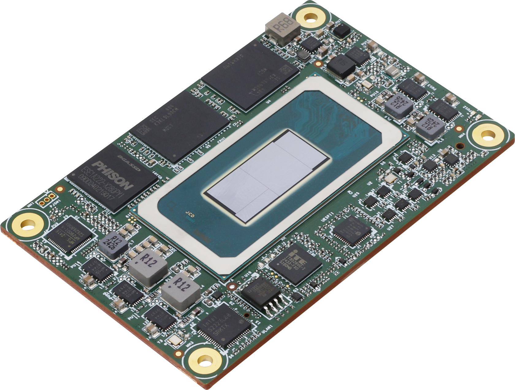
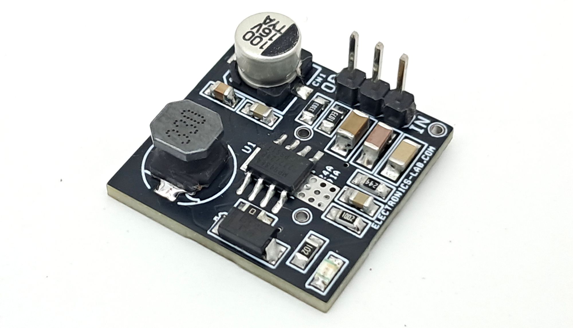
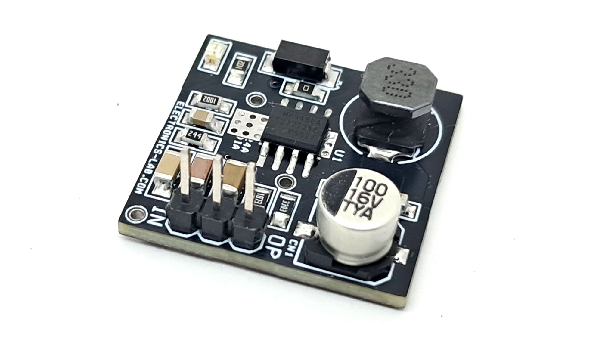
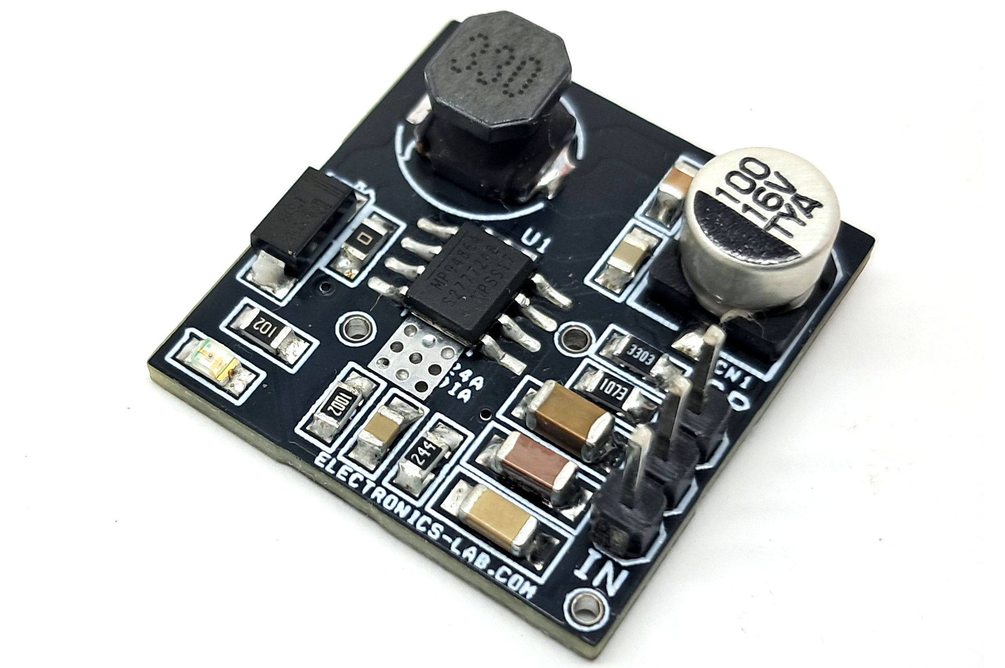
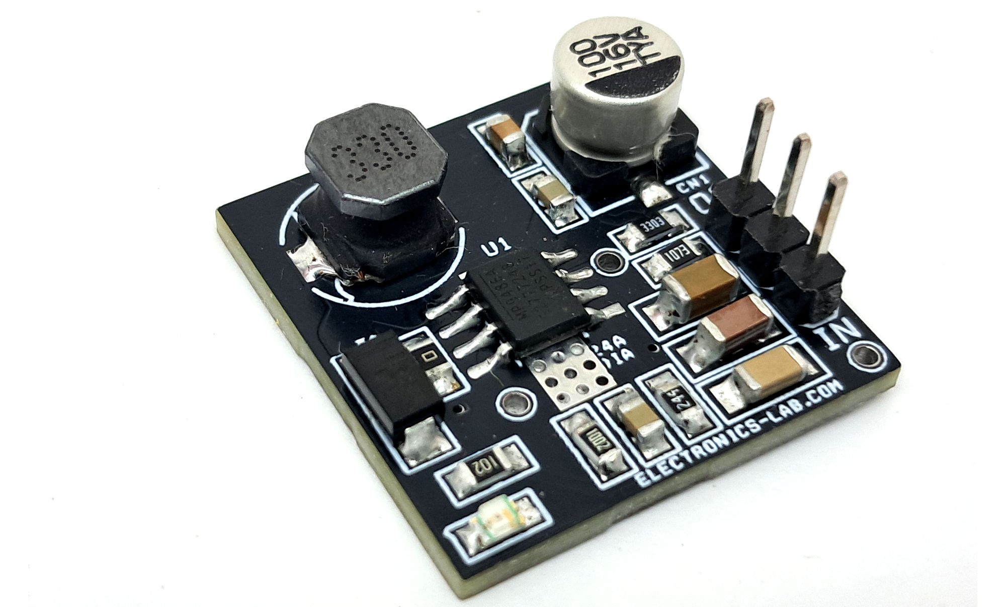
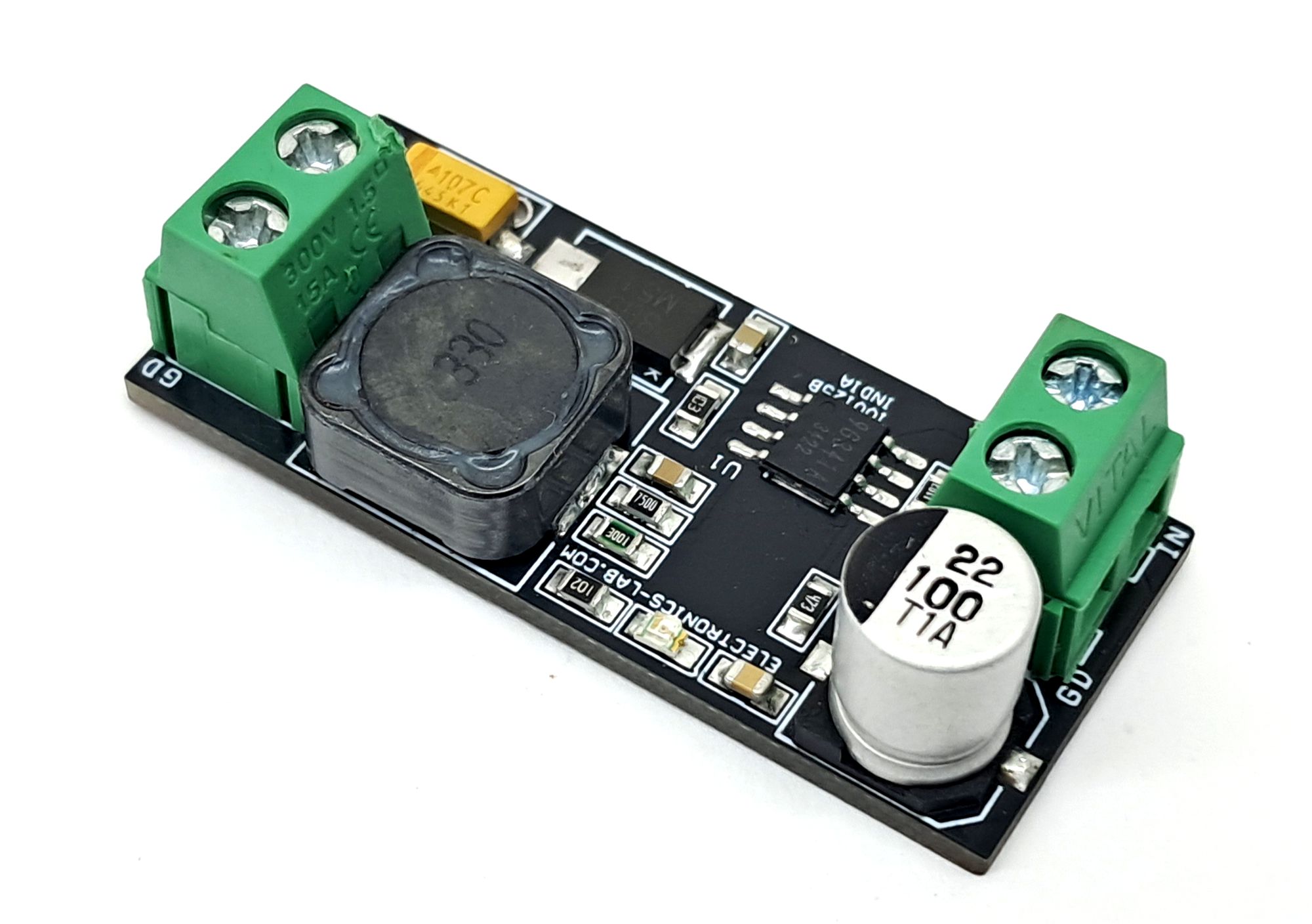
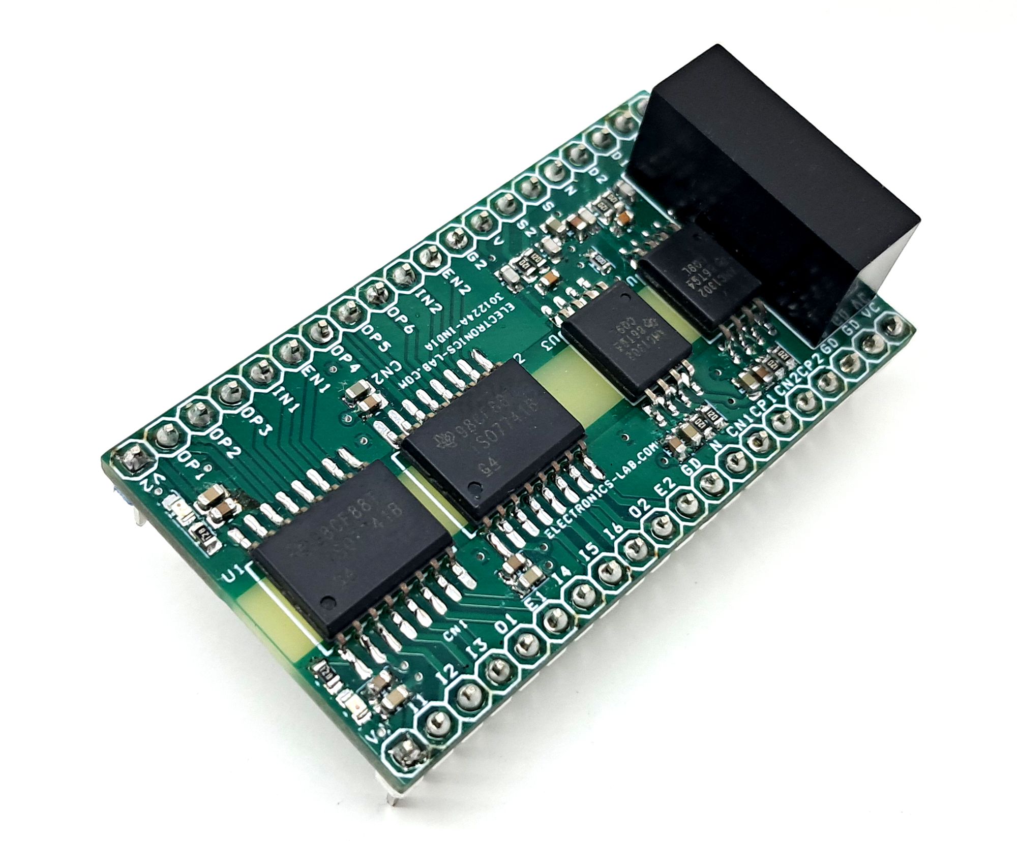
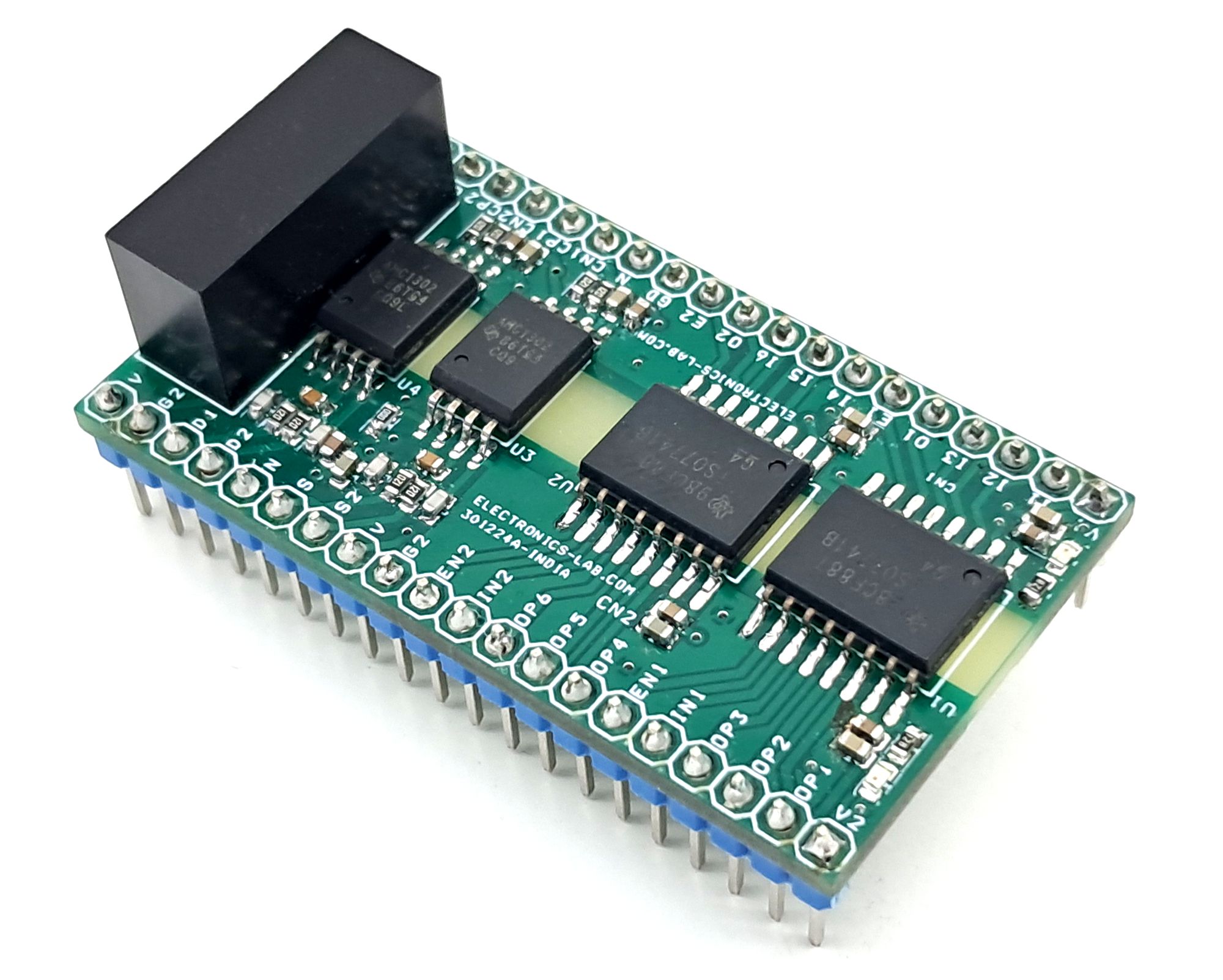
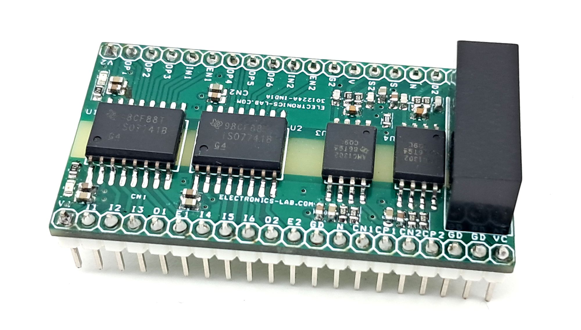
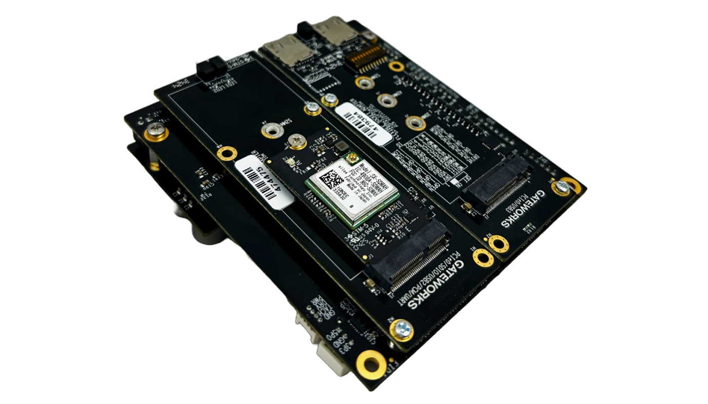
Morse Micro has teamed up with Gateworks Corporation to deliver the GW16159, a rugged, industrial-grade 802.11ah Wi-Fi HaLow M.2 radio module for long-range, low-power wireless communication in IoT applications.

Wi-Fi HaLow M.2 module

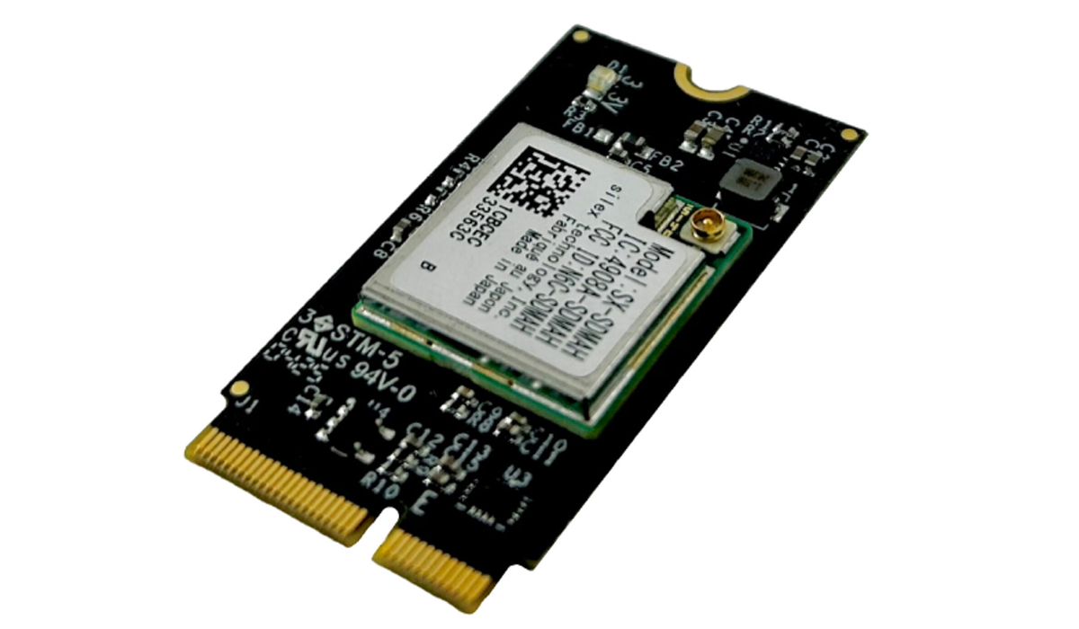
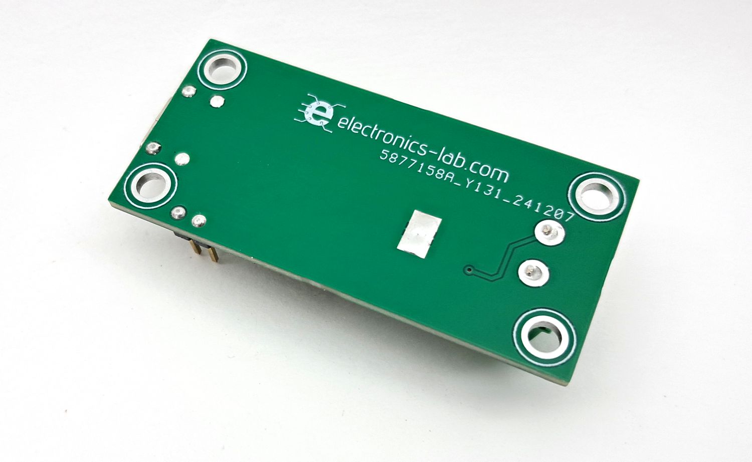
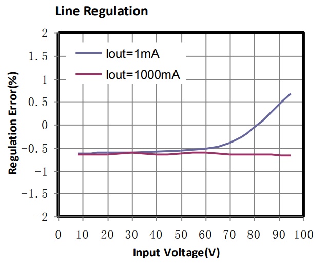
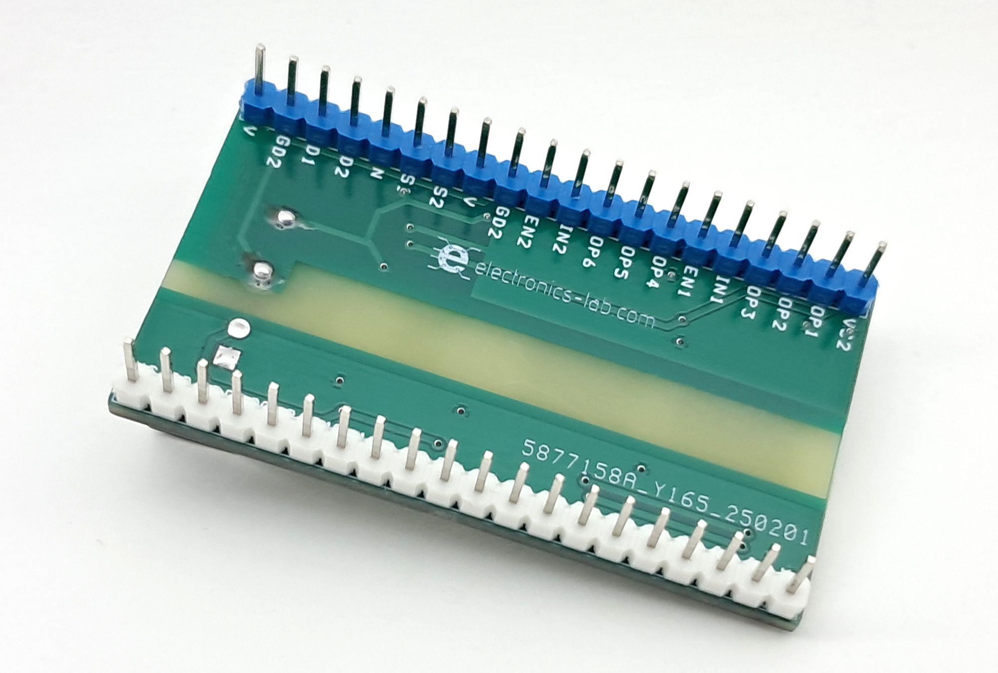
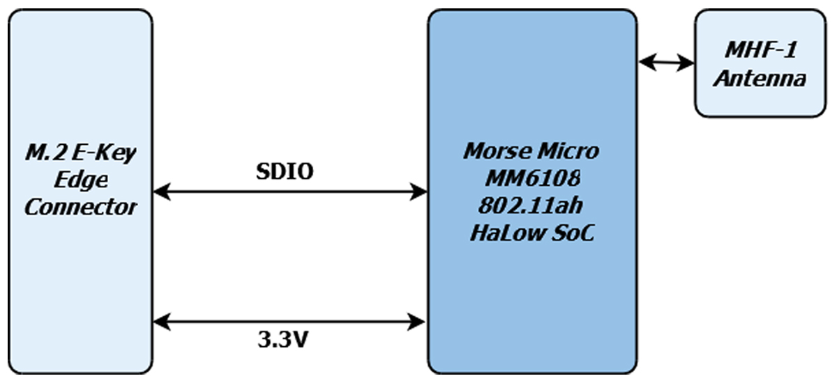
Specifically built for use with Gateworks VeniceFLEX single board computers, it connects via an M.2 E-Key 2242 interface using SDIO signalling—not compatible with standard Venice SBCs. The card features the Silex SX-SDMAH module, powered by the Morse Micro MM6108 SoC, and operates in the 902–928 MHz license-exempt band, offering improved building and foliage penetration compared to traditional Wi-Fi. It supports data rates of up to 32.5 Mbps, various bandwidth options (1/2/4/8 MHz), and multiple wireless modes (AP and station), along with security standards like WPA2-PSK and WPA3.

The radio supports simultaneous GATT client/server, FOTA, and over 100 clients, making it suitable for industrial IoT networks requiring long range (1 km+), low power, and robust performance. It is FCC certified, operates in temperatures from -40°C to +85°C, and supports standard Linux networking tools. A development kit (GW11056) is also available, which includes the GW16159 radio, VeniceFLEX SBC, antenna, and required accessories for quick deployment.

Previously, we have written about Seed Studio’s Mini-PCIe Wi-Fi HaLow Module, which is designed for industrial and embedded applications. You can check it for your reference.

GW16159 802.11ah Wi-Fi HaLow M.2 Module Specifications:

  • Wi-Fi Standard: IEEE 802.11ah (Wi-Fi HaLow)
  • Chipset:
    • Module: Silex SX-SDMAH
    • SoC: Morse Micro MM6108
  • Frequency Band: 902 – 928 MHz (license-exempt)
  • Data Rate: Up to 32.5 Mbps
  • Bandwidth Support: 1 / 2 / 4 / 8 MHz
  • Transmit Power Output: Up to +26.5 dBm
  • Wireless Modes: Access Point (AP) and Station (STA)
  • Security:
    • OPEN
    • WPA2-PSK (AES)
    • WPA3-OWE
    • WPA3-SAE
  • Misc:
    • Simultaneous GATT Server and Client
    • FOTA (Firmware Over-the-Air) support
    • Supports 100+ clients
  • Interface: SDIO Data Bus (compatible only with Gateworks VeniceFLEX SBCs)
  • Antenna Connector: MHF-1
  • Power Supply:
    • Input Voltage: 3.3V via M.2 Edge Connector
    • Operating Current: 0.1A Typical
  • Dimensions: 22.0x42x3.5mm
  • Weight: 0.22oz (6.2g) M.2 E-Key (2242) form factor
  • Operating Temperature: -40°C to +85°C
  • Humidity (non-condensing): 20% to 90%
  • Certification: FCC Certified

Wi-Fi HaLow M.2 module

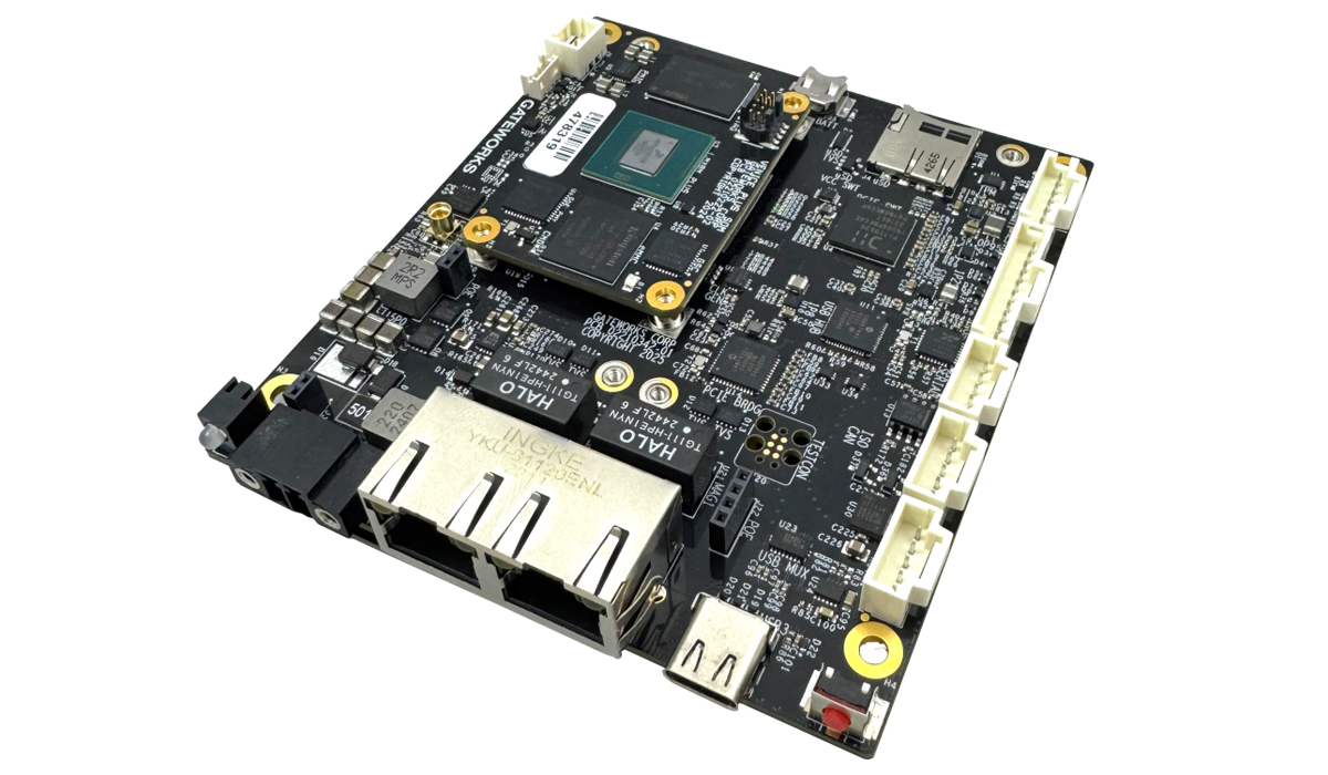
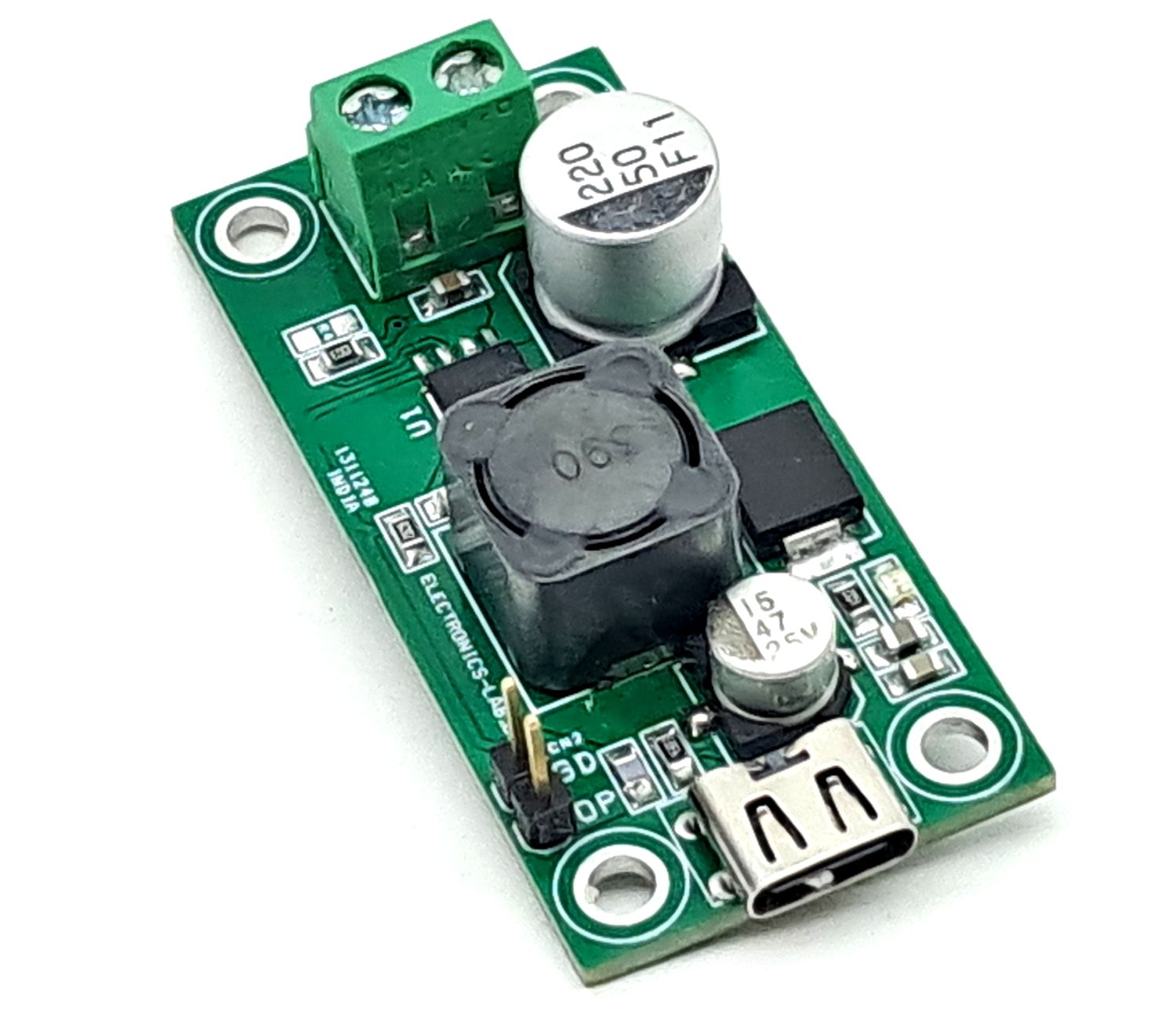
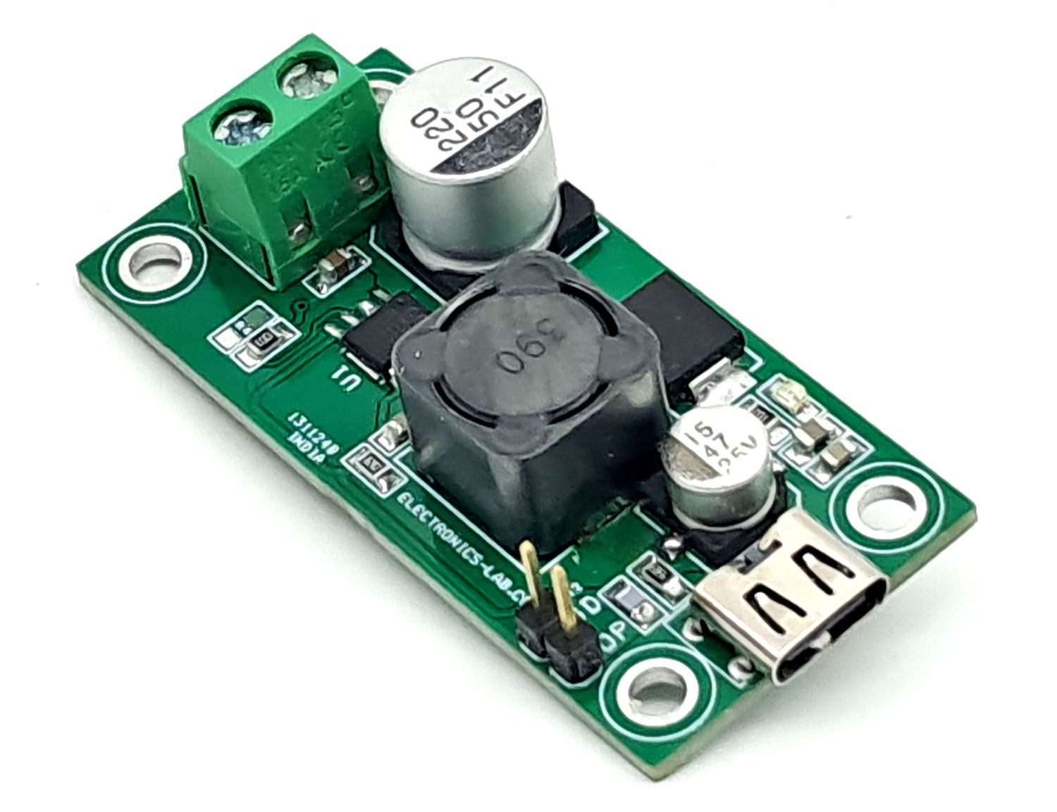
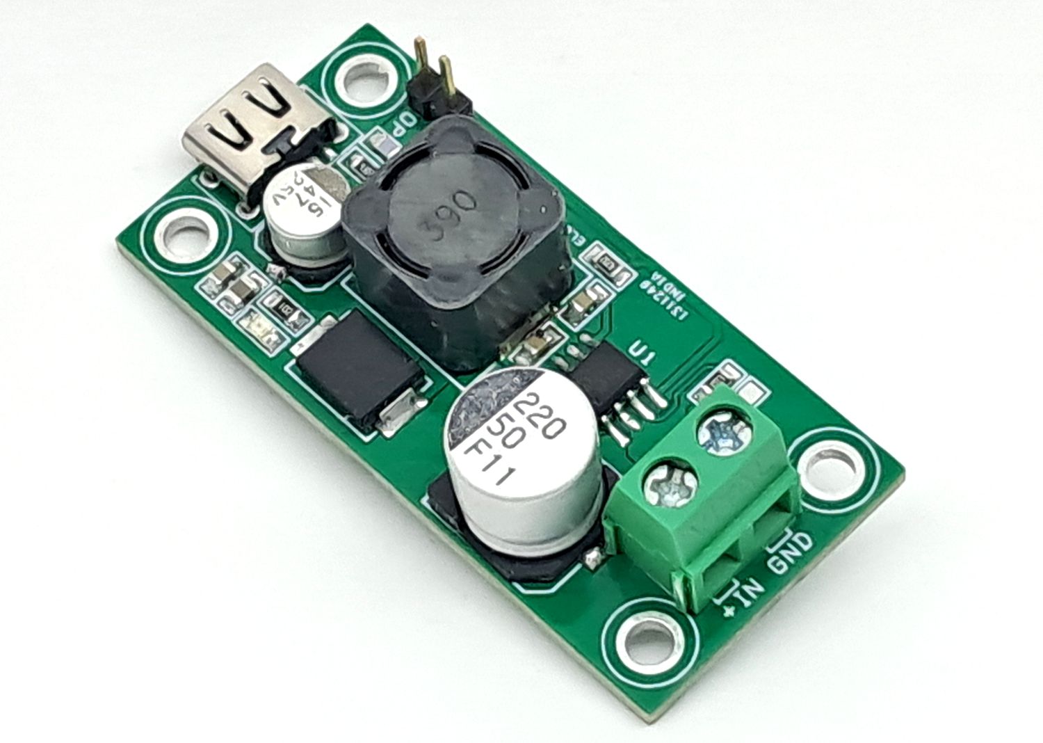
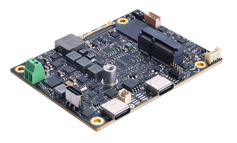
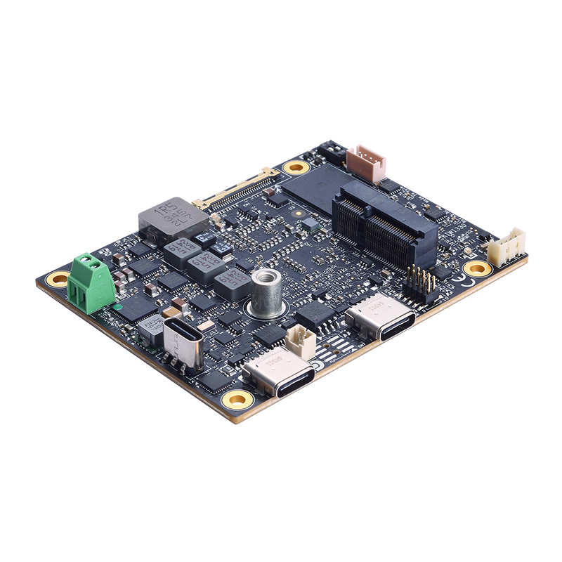
The GW11056 Wi-Fi HaLow Development Kit is an industrial-grade single board computer (SBC) platform designed to evaluate the 802.11ah Wi-Fi HaLow wireless standard using the included GW16159 M.2 card. Built around the Gateworks VeniceFLEX GW8200 SBC. The kit includes key components such as a JTAG adapter, antenna, adapter cables, and a power supply.

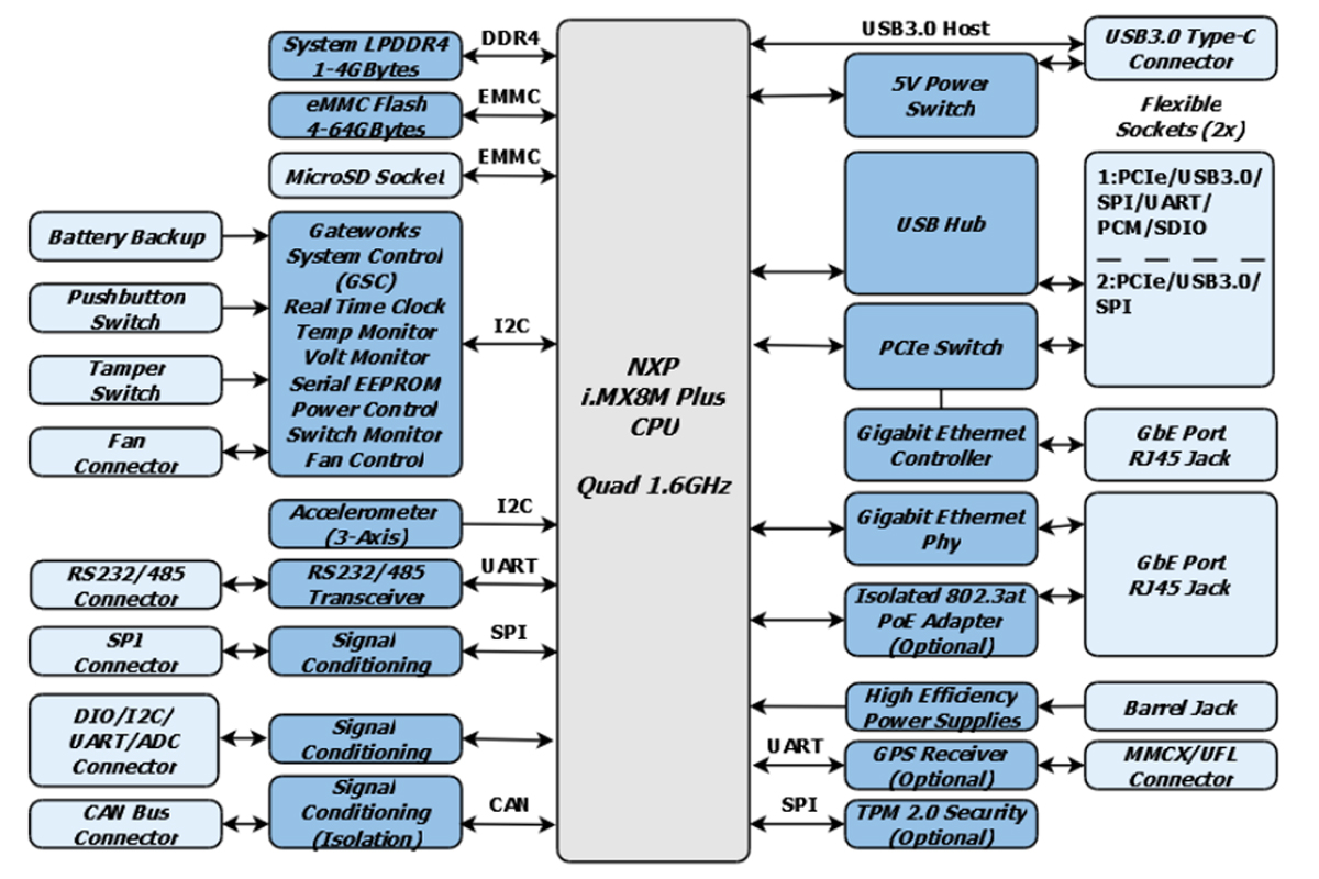
It features an NXP i.MX 8M Plus Quad-Core ARM Cortex-A53 processor, 4GB LPDDR4 RAM, 64GB eMMC flash, and dual Gigabit Ethernet ports with PoE support. It offers flexible expansion via Mini-PCIe and M.2 sockets for additional connectivity like Wi-Fi, cellular, BLE, or NVMe. The system also includes u-blox GPS and operates within a wide industrial temperature range (-40°C to +85°C).

GW8201-S21 SBC Block Diagram

GW11056 Wi-Fi HaLow Development Kit Specifications:

  • SBC: Gateworks GW8201-S21 based on NXP i.MX 8M Plus quad-core Cortex-A53 @ 1.6GHz
  • RAM: 4GB LPDDR4
  • Storage: 64GB eMMC flash
  • Wireless:
    • GW16159 Wi-Fi HaLow (802.11ah) M.2 card included
    • Flexible sockets for additional Wi-Fi, BLE, or cellular modules (Mini-PCIe, M.2)
  • Networking:
    • 2x Gigabit Ethernet ports
    • PoE support via GW168PB0 adapter (802.3at/af, isolated)
    • Dual Isolated CAN bus ports
  • GPS: u-blox GPS module with MMCX antenna connector
  • I/O Interfaces:
    • JTAG adapter for programming and serial console access
    • RS232/RS485 and TTL serial ports
    • I2C and SPI ports
    • Digital I/O and Analog input
  • Expansion:
    • Flexible Mini-PCIe and M.2 sockets for wireless or NVMe modules (15W Available)
      • FSA#1: USB 3.0, PCIe, SPI
      • FSA#2: USB 3.0, PCIe, I2C, SDIO, SPI, UART, PCM
      • GW16FE0: FSA to M.2 E-Key (Wi-Fi)
      • GW16FB0: FSA to M.2 B-Key (Modems)
  • USB: 1× USB Type-C 3.0 Host
  • Security: TPM 2.0 module
  • Misc:
    • RTC with battery backup
    • Watchdog timer
    • Voltage and temperature monitoring
    • Serial Configuration EEPROM
    • 3-axis digital MEMS accelerometer sensor
  • Power:
    • Input Voltage: 8 to 60V DC
    • Operating Current: 163mA Typical @ 24VDC
    • 4W @ 25°C Typical Operating Power
    • Power Through a Dedicated Connector or Ethernet with an optional isolated 802.3af/at Adapter
  • Dimensions: 90 x 100 x 21 mm
  • Weight: 80g
  • Operating Temperature: -40°C to +85°C (industrial grade)
  • Humidity (non-condensing): 20% to 90%

It comes pre-loaded with a Linux Ubuntu​ Board Support Package (Optional: OpenWrt, Yocto, Buildroot support), enabling immediate development and testing.

As per the official announcement, the GW16159 M.2 card and the GW11056 development kit are now available for purchase through Gateworks and its authorised distributors. The GW11056 kit is currently listed on DigiKey with a price of around $1,085.70, while the cost of the GW16159 module has yet to be revealed.

AAEON’s NanoCOM-MTU Hosts 28W Intel Core Ultra CPUs on the COM Express Type 10 Form Factor

The world’s first COM Express Type 10 module to host 28W CPUs from the Intel® Core™ Ultra line, the NanoCOM-MTU represents makes a big statement in a small form factor.

AAEON, a leading provider of Computer-on-Modules, has today announced the NanoCOM-MTU, a COM Express Type 10 CPU Module powered by Intel® Core™ Ultra processors. Available in SKUs equipped with either the Intel® Core™ Ultra 7 Processor 155H or Intel® Core™ Ultra 5 Processor 125H, both 28W, the NanoCOM-MTU offers up to 16 cores and 22 threads on the diminutive 84mm x 55mm form factor.

It is clear from the combination of high CPU performance and relatively low power consumption of its processor selection that the NanoCOM-MTU is catered towards customers that require a small, flexible, and scalable solution. This is particularly apparent in AAEON’s investment into the module’s memory and storage, where despite default SKUs offering 16GB of LPDDR5(X) and 128GB of NVMe, AAEON note there is the option of extending these to 32GB of LPDDR5(X) and 256GB of NVMe, respectively. By default, the NanoCOM-MTU also offers two SATA drives, while additional expansion is available via four PCIe 4.0 slots.

Key Features:

  • Choice of Intel® Core™ Ultra 7 Processor 155H or Intel® Core™ Ultra 5 Processor 125H
  • 16GB LPDDR5X and 128GB NVMe (optional: 32GB of LPDDR5(X) and 256GB of NVMe)
  • -20°C to 70°C temperature range & +9V to 19V power input range
  • OS Support: Windows® 11 (64-bit) and Linux Ubuntu 24.04.1 with Kernel 6.8

The largest advancement outside of the CPUs offered by the module are in its corresponding graphics package. Intel® Arc™ graphics support dual display outputs via both DDI and eDP outputs with resolutions of up to 3840 x 2160 at 60Hz. This configuration, along with the module’s high definition audio interface lends the NanoCOM-MTU to various application areas, with smart healthcare imaging, AI-assisted industrial inspection, and robotics all being suitable.

The NanoCOM-MTU contains a robust I/O, including a LAN port for Intel® Ethernet Controller I226-IT at 2.5GbE and multiple USB ports (eight USB 2.0 and two USB 3.2 Gen 2). Notably, the module also supports two MIPI CSI interfaces. In terms of serial communication, the module hosts two 2-Wire UART, an 8-bit GPIO, SMBus, and I2C, which lend the module to embedded industrial, robotic, and edge computing applications.

With respect to environmental resilience, the NanoCOM-MTU falls in line with the -20°C to 70°C minimum temperature tolerance range instituted for products from its embedded computing business unit in 2024. Meanwhile, the module offers operational stability in the form of a 9V to 19V input range for both ATX and AT power supplies.

The module supports multiple operating systems, including Windows® 11 (64-bit) and Linux Ubuntu 24.04.1 with Kernel 6.8, providing flexibility for developers in different environments.

For more information about the NanoCOM-MTU, please visit the AAEON website, or contact an AAEON representative directly.

48V DC Input DC-DC Converter – 5V USB C-Type Output

This DC-DC converter board is specifically designed as a USB C-Type power source, providing a stable 5V output with a maximum current up to 2A. The converter’s wide input voltage range of 4.5V to 48V ensures flexibility and compatibility with various power sources. Key features of the DC-DC converter include excellent load and line regulation, which enable it to maintain a stable output voltage despite changes in input voltage or load current. Additionally, the converter incorporates robust fault condition protection mechanisms, such as cycle-by-cycle current limiting and thermal shutdown, to prevent damage from overcurrent or overheating.

The circuit operates at a fixed frequency of 100kHz, ensuring efficient and reliable performance. For convenient connection, the board features screw terminals for the input supply and a USB-C connector for the output. An additional 2-pin header connector is also provided for alternative output access. Furthermore, an onboard LED indicator provides visual confirmation of the output status, allowing for easy monitoring and troubleshooting.

Features

  • Input Power 4.5V to 48V
  • Output 5V USB C-Type
  • Output Current Up to 2Amps
  • Operation Frequency 100Khz
  • On Board Output LED
  • Screw Terminal for Power Input
  • USB-C Type Connector for 5V Output
  • 2 Pin Header Connector Output 5V
  • 4X3MM PCB Mounting Holes
  • PCB Dimensions 52.71 x 24.77 mm

The MP2494 is a current-mode buck regulator. That is, the EA output voltage is proportional to the peak inductor current. At the beginning of a cycle SW is off; the EA output voltage is higher than the current sense amplifier output; and the current comparator’s output is low. The rising edge of the 100kHz CLK signal sets the RS Flip-Flop. Its output turns on SW thus connecting the SW pin and inductor to the input supply. The increasing inductor current is sensed and amplified by the Current Sense Amplifier. Ramp compensation is summed to Current Sense Amplifier output and compared to the Error Amplifier output by the Current Comparator. When the Current Sense Amplifier plus Slope Compensation signal exceeds the EA output voltage, the RS Flip-Flop is reset and the MP2494 reverts to its initial SW off state. If the Current Sense Amplifier plus Slope Compensation signal does not exceed the COMP voltage, then the falling edge of the CLK resets the Flip-Flop. The output of the Error Amplifier integrates the voltage difference between the feedback and the 0.8V bandgap reference. The polarity is such that an FB pin voltage lower than 0.8V increases the EA output voltage. Since the EA output voltage is proportional to the peak inductor current, an increase in its voltage increases current delivered to the output. An external Schottky Diode (D1) carries the inductor current when SW is off. Enable Control the MP2494 has an Enable control pin (EN). Drive EN above 1.8V to turn on the MP2494. Drive EN below 0.4V to turn it off. Tie EN to VIN for automatic start up.

Connections

  • CN1 Power Input: Pin 1 4.5V to 48V DC, Pin 2 = GND
  • CN2 Power Output: Pin 1 = 5V DC Output, Pin 2 = GND
  • CN3 USB C-Type: USB C Type 5V Output
  • D2 Output Power LED

Schematic

Parts List

NOQNTYREFDESCMANUFACTURERSUPPLIERSUPPLIER PART NO
11CN12 PIN SCREW TERMINAL PITCH 5.08MMPHOENIXDIGIKEY277-1247-ND
21C1220uF/50V ELEKTROLYTICPANASONICDIGIKEYPCE3921CT-ND
31C22.2uF/50V CERAMIC SMD SIZE 0805YAGEO/MURATADIGIKEY
41C322uF/10V CERMAIC SMD SIZE 0805YAGEO/MURATADIGIKEY
53C4,C7,C8100nF/50V CERAMIC SMD SIZE 0805YAGEO/MURATADIGIKEY
61C547uF/10-25V ELEKCTROLYTIC 6MM DIAWURTHDIGIKEY732-8416-1-ND
71C6150PF/50V CERAMIC SMD SIZE 0805YAGEO/MURATADIGIKEY
81D1MBRS360 SMD DIODE 60V 3AON SEMIDIGIKEYMBRS360T3GOSCT-ND
91D2LED RED SMD SIZE 0805OSRAMDIGIKEY475-1278-1-ND
101L139uH /4.2ABOURNS INCDIGIKEYSRR1210-390MCT-ND
111R1100K 5% SMD SIZE 0805YAGEO/MURATADIGIKEY
121R21K 5% SMD SIZE 0805YAGEO/MURATADIGIKEY
131R3430K 1% SMD SIZE 0805YAGEO/MURATADIGIKEY
141R4DNP
151R582K 1% SMD SIZE 0805YAGEO/MURATADIGIKEY
161U1MP2494 SOIC8MPS INCDIGIKEY1589-1596-1-ND
171CN3USB C-TYPE 6PIN SMDMOLEXDIGIKEY900-2171750001CT-ND
181CN22 PIN MALE HEADER PITCH 2.54MMWURTHDIGIKEY732-5315-ND

Connections

Block Diagram

Gerber View

Photos

Video

MP2494 Datasheet

Buck Converter for E-Scooters – 4.5V to 95V input – 5V output

This high-voltage buck converter is specifically designed for e-scooter and e-bike control power supply applications, but its versatility also makes it suitable for use in solar energy systems, automotive systems, and industrial power supplies. This converter utilizes the MPS9486 chip, a 4.5V-to-95V-input, 1A-output step-down converter that provides efficient power conversion.

The MP9486 chip employs a hysteresis voltage control method, which enables fast response to line or load transients, ensuring stable output voltage. Additionally, it integrates a high-side high-voltage power MOSFET with a current limit exceeding 1.7A, providing reliable and efficient power delivery.

The board is pre-configured for a 5V step-down application, making it an ideal solution for a wide range of applications that require a stable and efficient 5V power supply. With its robust design and high-performance capabilities, this high-voltage buck converter is an excellent choice for various power supply needs.

The output voltage of this board is set to 5V. With an input ranging from 8V (lower input may cause insufficient BST voltage) to 95V, this board can provide a load up to 1A.

Note: Due to the SCP mechanism MP9486 may start up into SCP mode if the load is on during startup and the turn-on threshold of the E-load is below 0.3V. To improve the startup capability, C3’s value should be greater.

Features

  • Input Supply 8V-To-95V Wide input Range
  • Output 5V DC
  • Output Current Up to 1A
  • Hysteretic Control: Simple Compensation
  • Frequency Up to 1Mhz
  • Hiccup mode Short Circuit Protection
  • Thermal Shutdown
  • PCB Dimensions 23.34 x 22.86 mm

Under-Voltage Lockout (UVLO)

Under-voltage lockout (UVLO) is implemented to protect the chip from operating at an insufficient supply voltage. The UVLO rising threshold is about 4V, while its falling threshold is a consistent 3.6V.

Thermal Shutdown

Thermal shutdown is implemented to prevent the chip from operating at exceedingly high temperatures. When the silicon die temperature is higher than its upper threshold, the entire chip shuts down. When the temperature is lower than its lower threshold, the chip is enabled again.

Output Short Protection

The output voltage is well-regulated when VFB is around 200mV. If the output is pulled low in over-current protection (OCP) or is shorted to GND directly, VFB is low, even though the power MOSFET is turned on. The MP9486 regards the low VFB as a failure. The power MOSFET shuts off if the failure time is longer than 10µs.  The MP9486 attempts operation again after a delay of about 300µs.  The power MOSFET current is also accurately sensed via a current sense MOSFET. If the current is over the current limit, the IC is shut down. This offers extra protection under output short conditions

Hysteresis Current Control with Adaptive

Threshold Adjustment the MP9486 operates in a hysteretic voltage control mode to regulate the output voltage. FB is connected to the tap of a resistor divider, which determines the output voltage. The power MOSFET is turned on when the FB voltage (VFB) drops to 185mV and remains on until VFB rises to 215mV. The power MOSFET is turned off when VFB rises to 215mV and remains off until VFB falls to 185mV. The two thresholds of 215mV and 185mV are adjusted adaptively to compensate for all the circuit delays, so the output voltage is regulated with an average 200mV value at FB.

Connections

  • CN1: Pin 1 = 8V To 95V DC Input, Pin 2 = GND, Pin 3 = 5V DC Output
  • D2: Power LED (Output)

Schematic

Parts List

NO.QNTY.REF.DESCMANUFACTUERERSUPPLIER SUPPLIER PART NO
11CN13 PIN MALE HEADER PITCH 2.54MMWURTHDIGIKEY732-5316-ND
22C1,C5100nF/50V CERAMIC SMD SIZE 0805YAGEO/MURATADIGIKEY
31C2100nF/100V CERAMIC SMD SIZE 1206YAGEO/MURATADIGIKEY
41C34.7uF/100V CERAMIC SMD SIZE 1206YAGEO/MURATADIGIKEY
51C41.5uF/100V CERAMIC SMD SIZE 0805YAGEO/MURATADIGIKEY
61C6100uF/10-16V ELEKCTROLYTIC OR TENTLUMWURTHDIGIKEY732-8490-1-ND
71C74.7uF/10V SMD SIZE 08905YAGEO/MURATADIGIKEY
81D1B1100/B OR ES1BDIODE INCDIGIKEYB1100-FDICT-ND
91D2LED SMD SIZE 0805OSRAMDIGIKEY475-1278-1-ND
101L133uH/1.7A 8MMABRACONDIGIKEY535-13623-1-ND
111R110K 1% SMD SIZE 0805YAGEO/MURATADIGIKEY
121R20E 5% SMD SI8ZE 0805YAGEO/MURATADIGIKEY
131R3240K 1% SMD SIZE 0805YAGEO/MURATADIGIKEY
141R4330K 5% SMD SIZE 0805YAGEO/MURATADIGIKEY
151R51K 5% SMD SIZE 0805YAGEO/MURATADIGIKEY
161R6107K 1% SMD SIZE 0805YAGEO/MURATADIGIKEY
171U1MP9486 SOIC8MPS INCDIGIKEY1589-1747-1-ND

Connections

Typical Application

Load Regulation

Line Regulation

Efficiency

Block Diagram

Gerber View

Photos

Video

MPS9486 Datasheet

Buck Converter 12V-76V Input, 5V DC Output

A buck converter board has been developed utilizing the BD9G341AEFJ, a non-synchronous DC/DC converter. This board accepts a wide input voltage range of 12V to 76V DC and generates a regulated 5V DC output. The BD9G341AEFJ features an integrated 150mΩ N-channel MOSFET and a programmable switching frequency, adjustable from 50kHz to 750kHz. On this board, the switching frequency is fixed at 200kHz using resistor R5. To ensure reliable operation, the board incorporates several protection features. A fixed soft-start circuit minimizes inrush current during startup. Additionally, the board includes Under-Voltage Lockout (UVLO), Thermal Shutdown Detection (TSD), Over-Current Protection (OCP), and Over-Voltage Protection (OVP) circuits. The UVLO threshold and hysteresis are configured externally using resistors R1 and R4 connected to the EN (Enable) pin.

Note: A cooling system is necessary when operating at a full load current of 3A to dissipate the heat.

Features

  • Input 12V to 76V DC
  • Output 5V DC
  • Output Current 2A, up to 3A (Read Note)
  • Operating Frequency 200Khz
  • On Board Power LED
  • Precision EN/UVLO Threshold +/-3%
  • Under Voltage Lockout (UVLO), Threshold 11V
  • Soft Start Function (20mS)
  • Over Current Protection (OCP)
  • Thermal Shutdown (TSD)
  • Over Voltage Protection (OVP)
  • Screw Terminals for Power Input and Output
  • PCB Dimensions 45.09 x 19.84 mm

The BD9G341AEFJ is a buck switching regulator with an integrated 150mΩ power MOSFET. Current mode architecture provides fast transient response and a simple phase compensation setup. The operating frequency is programmable from 50kHz to 750kHz. Additional protection features are included, such as Over Current Protection, Thermal shutdown,n and Under voltage lockout.  The under-voltage lockout and hysteresis can be set by an external resistor.

UVLO

This is a Low Voltage Error Prevention Circuit. This prevents internal circuit error during increase of Power Supply Voltage and during decline of Power supply Voltage. It monitors VCC Pin Voltage and internal REG Voltage, When VCC Voltage becomes 11V and below, UVLO turns OFF all Output FET and turns OFF the DC/DC Comparator Output, and the Soft Start Circuit resets. Now this Threshold has Hysteresis of 200mV.

OSC

This block generates inner CLK. The internal oscillator is set with a single resistor connected between this pin and the GND. RT pin connects to 47kohm, frequency is set 200 kHz.

EN Shutdown function.

If the voltage of this pin is below 1.3V, the regulator will be in a low power state. If the voltage of this pin is between 1.3V and 2.4V will be standby mode. If the voltage of this pin is above 2.6V, the regulator is operational. An external voltage divider resistor R1 and R4 used to set under voltage threshold.

OCP Over current protection

If the current of power MOSFET is over 6.0A (typ), this function reduces duty pulse –by- pulse and restricts the over current. If IC detects OCP 2 times sequentially, the device will stop and after 20 msec restart.

TSD (Thermal Shutdown)

This is Thermal Shutdown Detection When it detects an abnormal temperature exceeding Maximum Junction Temperature (Tj=150°C), it turns OFF all Output FETs, and turns OFF the DC/DC Comparator Output. When Temperature falls, and the IC automatically returns

OVP Over voltage protection

Output voltage is monitored with FB terminal, and output FET is turned off when it becomes 120% of set-point voltage.

Connections

  • CN1: Pin 1 = + DC Input 12V-76VDC, Pin 2 = GND
  • CN2: Pin 1 = +5V DC Output, Pin 2 = GND
  • D1: Power LED

Schematic

Parts List

NO.QNTY.REF.DESC.MANUFACTURERSUPPLIERSUPPLIER PART NO
12CN1,CN22 PIN SCREW TERMINAL PITCH 5.08MMPHOENIXDIGIKEY277-1247-ND
21C122uF/100V ELECTROLYTIC 8MMNICHICONDIGIKEY493-6433-1-ND
31C2100nF/100VYAGEO/MURATADIGIKEY
41C3100uF/6.3V TANTLUM SMD SIZE 1210/1411KYOCERADIGIKEY478-13510-1-ND
51C46800PF/50V CERAMIC SMD SIZE 0805YAGEO/MURATADIGIKEY
61C5DNP
71C622uF/10V CERAMIC SMD SIZE 0805YAGEO/MURATADIGIKEY
81D1SS8PH9VISHAYDIGIKEYSS8PH9-M3/87AGICT-ND
91D2LED RED SMD SIZE 0805OSRAMDIGIKEY475-1278-1-ND
101L133uH/4.2A 12MMX12MM 7447709330WURTHDIGIKEY732-1244-1-ND
111R1110K 1% SMD SIZE 0805YAGEO/MURATADIGIKEY
121R23K 1% SMD SIZE 0805YAGEO/MURATADIGIKEY
131R3750E 1% SMD SIZE 0805YAGEO/MURATADIGIKEY
141R427K 1% SMD SIZE 0805YAGEO/MURATADIGIKEY
151R547K 1% SMD SIZE 0890YAGEO/MURATADIGIKEY
161R610K 1% SMD SIZE 0805YAGEO/MURATADIGIKEY
171R71K 5% SMD SIZE 0805YAGEO/MURATADIGIKEY
181U1BD9G341AEFJROHMDIGIKEYBD9G341AEFJ-E2CT-ND

Connections

Gerber View

Photos

Video

BD9G341AEFJ Datasheet

8 Channel Digital – 2 Channel Analog Isolator Module

The project presented here features an 8-channel digital and 2-channel analog isolator. The board is equipped with 6 forward digital isolators and 2 reverse digital isolators, in addition to 2 analog isolators.

The digital isolators boast an impressive 5000 VRMS isolation rating, as per UL1577 standards. Meanwhile, the analog isolators are certified to provide reinforced galvanic isolation of up to 5 kVRMS, adhering to VDE V 0884-11 and UL1577 standards. Furthermore, they support a working voltage of up to 1.5 kVRMS. The digital isolators are capable of supporting data rates of up to 100 Mbps.

Features

  • Power Input 5V DC
  • Level Translation Range: 2.25V to 5.5V
  • 2 x Power LED Low Side and High Side
  • 6 Channel Forward, 2 Channel Reverse Digital Isolator
  • 2 Channel Analog Isolator (Current and Voltage Sense)
  • Analog Output (Differential Signal)
  • 100 Mbps data rate (Digital Isolator)
  • Header Connector provided to access Digital I/Analog and Power Input and Output
  • Robust isolation barrier
  • 100-year projected lifetime at 1500 VRMS working voltage
  • Up to 5000 VRMS isolation rating
  • Up to 12.8 kV surge capability
  • ±100 kV/µs typical CMTI
  • Default output high (Digital)
  • PCB dimensions: 4 51.44 x 28.73 mm

The 8-channel digital isolator

The board consists of 2 x ISO7741 chips, which provide 6 channels of forward digital isolation and 2 channels of reverse digital isolation. Notably, all outputs are normally high, and the ENABLE pins can be used to disable them. By connecting the Enable 1 and Enable 2 pins to GND on their respective sides, all outputs can be put in a LOW state, effectively disabling them. In the event of input power or signal loss, the output will default to a high state. The level translation range for these isolators is between 2.25V and 5.5V. Additionally, they exhibit high electromagnetic immunity, reducing noise and preventing high voltages from traveling to the main unit.

  • Output enables 1. Output pins on side 1 are enabled when EN1 is high or open and in high-impedance state when EN1 is low.
  • Output enables 2. Output pins on side 2 are enabled when EN2 is high or open and in high-impedance state when EN2 is low.

2 Channel Precision, ±50-mV Input, Reinforced Isolated Amplifier (AMC1302)

The board also consists of 2 x channel AMC1302 analog isolated Amplifiers with ±50-mV Inputs; these amplifiers can be used to measure the current as well as voltage. The output is differential and can be directly interfaced to the ADC of the host.

Power Supply

The board features a 5V input, 5V output isolated DC-DC converter, where the input side is connected to the low-side power (host side) and the output is connected to the high-side. The system operates with a 5V power supply on both sides of the isolation barrier. However, if the supply range differs, it is recommended to replace the DC-DC converter to ensure compatibility with the specific power requirements. Additionally, the digital and analog isolators on the board support both 5V and 3.3V supplies on the high-side and low-side, providing flexibility in terms of voltage compatibility

  • Low-Side (Host/Micron troller) Side 5V, High-Side 5V Use B0505S-2WR3 DC-DC Converter (Input 5V, Output 5V)
  • Low-Side (Host/Micron troller) Side 5V, High-Side 3.3V Use B0503S-2WR3 DC-DC Converter (Input 5V, Output 3.3V)
  • Low-Side (Host/Micron troller) Side 3.3V, High-Side 3.3V Use B0303S-2WR3 DC-DC Converter (Input 5V, Output 3.3V)

Analog Input

The differential amplifier input stage of the AMC1302 feeds a second-order, switched-capacitor, feed-forward ΔΣ modulator. The gain of the differential amplifier is set by internal precision resistors with a differential input impedance of RIND. The modulator converts the analog input signal into a bitstream that is transferred across the isolation barrier, as described in the Isolation Channel Signal Transmission section. There are two restrictions on the analog input signals INP and INN. First, if the input voltages VINP or VINN exceed the range specified in the Absolute Maximum Ratings table, the input currents must be limited to the absolute maximum value, because the electrostatic discharge (ESD) protection turns on. In addition, the linearity and parametric performance of the device are ensured only when the analog input voltage remains within the linear full-scale range (VFSR) and within the common-mode input voltage range (VCM) as specified in the Recommended Operating Conditions table.

Analog Output

The AMC1302 offers a differential analog output comprised of the OUTP and OUTN pins. For differential input voltages (VINP – VINN) in the range from –50 mV to 50 mV, the device provides a linear response with a nominal gain of 41. For example, for a differential input voltage of 50 mV, the differential output voltage (VOUTP – VOUTN) is 2.05 V. At zero input (INP shorted to INN), both pins output the same common-mode output voltage VCMout, as specified in the Electrical Characteristics table. For absolute differential input voltages greater than 50 mV but less than 64 mV, the differential output voltage continues to increase in magnitude but with reduced linearity performance. The outputs saturate at a differential output voltage of VCLIPout, as shown in Figure, if the differential input voltage exceeds the VClipping value.

The AMC1302 is a precision, isolated amplifier with an output separated from the input circuitry by an isolation barrier that is highly resistant to magnetic interference. This barrier is certified to provide reinforced galvanic isolation of up to 5 kVRMS according to VDE V 0884-11 and UL1577, and supports a working voltage of up to 1.5 kVRMS. The isolation barrier separates parts of the system that operate on different common-mode voltage levels and protects the low-voltage side from hazardous voltages and damage. The input of the AMC1302 is optimized for direct connection to a low-impedance shunt resistor or other low-impedance voltage source with low signal levels.  The excellent DC accuracy and low temperature drift supports accurate current control in PFC stages, DC/DC converters, AC-motor and servo drives over the extended industrial temperature range from –40°C to +125°C

The ISO7741 device is a high-performance, quad-channel digital isolator with 5000 VRMS isolation ratings per UL 1577. This family includes devices with reinforced insulation ratings according to VDE, CSA, TUV, and CQC. The ISO7741B device is designed for applications that require basic insulation ratings only. The ISO7741 device provides high electromagnetic immunity and low emissions at low power consumption while isolating CMOS or LVCMOS digital I/Os. Each isolation channel has a logic input and output buffer separated by a double capacitive silicon dioxide (SiO2) insulation barrier. These devices come with enable pins which can be used to put the respective outputs in high impedance for multi-master driving applications and to reduce power consumption. The ISO7741 device has three forward and one reverse-direction channel.

Connections

  • CN1: Pin1= V1 5V DC Input, Pin 2 = Digital Input 1, Pin 3 = Digital Input 2, Pin 4 = Digital Input 3, Pin 5 = Digital Output 1L, Pin 6 = Enable 1L, Pin 7 = Digital Input 4, Pin 8 = Digital Input 5, Pin 9 = Digital Input 6, Pin 10 = Digital Output 2L, Pin 11 = Enable L2, Pin 12= GD-L, Pin 13 = NC, Pin 14 = CN1, Pin15= CP1, Pin 16 = CN2, Pin 17 = CP2, Pin 18 GD-L, Pin 19 = GD-L, Pin 20 = VC 5V DC Input
  • CN2: Pin 1 = V2 5V DC, Pin 2 = Digital Output 1H, Pin 3 = Digital Output 2H, Pin 4 = Digital Output 3H, Pin 5 = Digital Input 1H, Pin 6 = Enable 1H, Pin 7 = Digital Output 4H, Pin 8 = Digital Output 5H, Pin 9 = Digital Output 6H, Pin 10 = Input 2H, Pin 11=Enable 2H, Pin 12 = GD-H, Pin 13=V 5V DC, Pin 14 = VINP-S2, Pin 15 = VINN-S1, Pin 16=NC, Pin 17 =VINP-D2, Pin 18 = VINN-D1, Pin 19=GD-H, Pin 20 = V 5V DC
  • D1: Power LED V1 (Digital Isolator Low-Side)
  • D2: Power LED V2 (Digital Isolator High-Side)

Schematic

Parts List

NO.QNTY.REF.DESC.MANUFACTURINGSUPPLIER SUPPLIER PART NO
12CN1,CN2SIP20WURTHDIGIKEY732-5329-ND
27C1,C3,C5,C7,C10,C15,C2010uF/10V CERAMIC SMD SIZE 0603YAGEO/MURATADIGIKEY
37C2,C4,C6,C8,C11,C16,C19100nF/10V CERAMIC SMD SIZE 0603YAGEO/MURATADIGIKEY
42C9,C1410nF/10V CERAMIC SMD SIZE 0603YAGEO/MURATADIGIKEY
54C12,C13,C17,C18DNP
62D1,D2LED RED SMD SIZE 0603DIGIKEY5962-XL-1608SURC-06TR-ND
72R1,R21K 5% SMD SIZE 0605YAGEO/MURATADIGIKEY
84R3,R6,R8,R1110E 5% SMD SIZE 0603YAGEO/MURATADIGIKEY
95R4,R5,R7,R9,R100E SMD SIZE 0603YAGEO/MURATADIGIKEY
102U1,U2ISO7741DWRTIDIGIKEY296-47781-1-ND
112U3,U4AMC1302TIDIGIKEY296-50923-1-ND
121U5B0505S-2WR3 DC-DC CONVERTER 5V IN, 5V OUTMORNSUNDIGIKEY2725-B0505S-2WR3-ND

Connections

Diagrams


Gerber View

Photos

Video

ISO7741 Datasheet

Axiomtek Launches KIWI330: Ultra-Compact 1.6″ SBC with LPDDR5, NVMe, and Type-C DisplayPort for Edge AIoT

Axiomtek – a world-renowned leader relentlessly devoted to the research, development, and manufacture of innovative, highly efficient, and reliable industrial computer products – is pleased to introduce the KIWI330, an ultra-compact 1.6” embedded board built to accelerate AIoT development and streamline device integration. Powered by the Intel® processor N50, the KIWI330 is equipped with 4GB of onboard LPDDR5 memory and a 64GB NVMe SSD, delivering energy-efficient performance in an ultra-small form factor — ideal for space-constrained applications. With its high integration, flexible expansion capabilities, and consistent industrial-grade quality, the KIWI330 is the perfect solution for developers building the next generation of compact AIoT systems.

“The KIWI330 is purpose-built for developers who require performance, modularity, and compactness in a single reliable embedded board,” said Irene Su, Product Manager of the IDS Division at Axiomtek. “With powerful computing capabilities, USB Type-C expandability, and flexible MIO module support, the KIWI330 significantly shortens development cycles and time to market.”

Advanced Features of KIWI330

  • Ultra-compact 1.6-inch embedded board
  • Intel® processor N50 onboard
  • Onboard 4GB LPDDR5 memory
  • Onboard 64GB NVMe SSD storage
  • Supports M.2 Key E socket for wireless modules or AI accelerators
  • Supports eDP for high-resolution display applications
  • Supports operating system: Linux, Windows®

Despite its small footprint, the KIWI330 offers rich connectivity, including two USB 3.2 Type-C ports — one horizontal with DisplayPort support — and an M.2 Key E 2230 slot for wireless modules or AI accelerators. and an M.2 Key E 2230 slot for wireless modules or AI accelerators. The board also supports eDP for high-resolution embedded display applications. For system integrators with diverse application needs, the KIWI330 also supports optional MIO expansion modules, enabling effortless addition of COM, LAN, or GPIO ports while maintaining a compact system design.

The integrated LPDDR5 memory and NVMe SSD provide high-speed performance and energy efficiency, eliminating the need for external storage modules. With comprehensive middleware support, hardware monitoring capabilities, and compatibility with both Windows® and Linux®, the KIWI330 is well-suited for a wide range of embedded applications, including robotics, smart devices, industrial automation, edge AI computing, and intelligent gateway solutions.

The 1.6″ SBC KIWI330 is available now. For more product information or pricing, please visit our global website at www.axiomtek.com or contact one of our sales representatives at info@axiomtek.com.tw.

Radxa eMMC/UFS Module Reader Lets You Flash Storage via USB 3.0 Adapter

eMMC UFS module reader

The eMMC/UFS Module Reader from Radxa is a compact and versatile USB 3.0 adapter designed to read and write data from eMMC and UFS storage modules, specifically tailored for development boards like the Radxa ROCK series. It enables easy flashing, backup, or data recovery by connecting the storage module to a standard PC via USB. The reader supports both eMMC 5.1 and UFS 2.1 modules and is backwards compatible with older versions.

eMMC UFS module reader

A USB 3.0 Type-C port for fast data transfer is featured, and a switch is included to easily switch between eMMC and UFS modes, making it handy for developers and testers. This module is really helpful for embedded projects, and you can flash or debug OS images without turning on the board. It’s easy to use, works with many systems, and is a good add-on if you’re using Radxa boards or something like that.

eMMC/UFS Module Reader Specifications:

  • Interface: USB 3.0 Type-C
  • Supported Storage Modules:
    • eMMC (up to eMMC 5.1)
    • UFS (up to UFS 2.1)
  • Mode Switch: Manual toggle between eMMC and UFS modes
  • Other: Designed for developers and users of Radxa SBCs such as ROCK 5B, ROCK 3, etc.
  • Dimensions: Compact form factor (not specified)

The company also mention, this adapter also supports modules used in boards like PINE64 and Odroid. It uses a dual-lock connector for steady, repeated use and works without any drivers on Windows, Linux, macOS, and HarmonyOS. It supports advanced modes like eMMC HS400 and UFS HS-Gear3B, enabling it to work well with various systems and providing low-level access.

Radxa UFS Module

The company also offers a UFS Module, a high-speed storage module designed for use with Radxa single-board computers (SBCs) that support UFS (Universal Flash Storage). Faster data transfer and better performance are offered compared to traditional eMMC storage. It comes in different sizes, from 64GB up to 1TB, and there’s also a version that can handle tough conditions, like really hot or cold temperatures, for outdoor or rough use.

It’s built with UFS 3.1 technology, comes in multiple storage capacities and connects directly to the SBC through a dedicated interface, making it suitable for booting operating systems, running applications, or storing large files. This UFS module is mainly used in embedded systems, development boards, and performance-focused projects where fast storage is important.

Radxa UFS Module Specifications:

  • Storage Type: Universal Flash Storage (UFS) 2.1
  • Capacities: Available in 64GB, 128GB, 256GB, 512GB, and 1TB
  • Interface: UFS connector compatible with Radxa boards (e.g. ROCK 5 series)
  • Performance:
    • Sequential Read: Up to 850 MB/s
    • Sequential Write: Up to 250 MB/s
  • Power:
    • Operating Voltage: 3.3V
    • Power Consumption: Low power usage during operation and idle
  • Dimensions: Custom compact Form Factor for Radxa SBCs
  • Boot Support: Can be used as bootable storage
eMMC UFS module reader
Hardware Connection

Radxa UFS Module is the pair with this UFS/eMMC Module Reader. It features a compact form factor, low power usage, and supports high-speed read/write operations. That makes it ideal for developers who need reliable and efficient storage for testing or final deployment.

Radxa says these modules aren’t tied to any specific chip and can work with boards using Allwinner, Rockchip, MediaTek, or Qualcomm. They also fit well with Radxa boards like the ROCK 4D, CM4 IO, Cubie A7A, and even the upcoming Dragon Q6A.

At the time of writing, AliExpress lists the eMMC/UFS Module Reader for about $14.22. The UFS Module starts at $11.35 to $31.45 for up to the 256 GB variant. More information of the Radxa eMMC/UFS Combo Module Reader is available on the documentation website.

GL.iNet GL-BE9300 tri-band WiFi 7 router ships with 5x 2.5GbE ports, OpenWrt, and VPN support

GL.iNet Flint 3 (GL-BE9300) is a budget-friendly tri-band WiFi 7 BE9300 router designed for advanced home and small office networking, offering fast wireless performance and multiple high-speed wired connections. The most interesting thing is that it integrates features typically found in premium routers, like support for VPNs, load balancing, and failover.

Powered by a 1.5 GHz Qualcomm quad-core processor, the router includes 1GB DDR4 RAM, 8GB eMMC storage, and runs a customized OpenWrt v23.05 system. It supports tri-band WiFi 7 (2.4GHz @ 688Mbps, 5GHz @ 2882Mbps, 6GHz @ 5765Mbps), five 2.5GbE ports (one WAN, one WAN/LAN, and three LAN), and a USB 3.0 port for tethering or cellular dongles. VPN support includes WireGuard and OpenVPN-DCO with up to 680Mbps throughput. Additional features include AdGuard Home, ZeroTier, Tailscale, cloud access via GoodCloud and AstroWarp, and a dual-color LED. It operates within 0–40°C and ships with the required accessories, making it ideal for users needing reliable, high-throughput wired and wireless networking.

GL.iNet Flint 3 (GL-BE9300) tri-band router specifications:

  • Processor
    •  Qualcomm quad-core processor @ 1.5GHz (likely IPQ5332)
  • Memory
    •  1GB DDR4
  • Storage
    •  8GB eMMC flash
  • Wireless:
    • Tri-band WiFi 7 (802.11be)
    • 2.4GHz up to 688Mbps
    • 5GHz up to 2882Mbps
    • 6GHz up to 5765Mbps
    • 4x foldable external antennas
  • Ethernet:
    • 1x 2.5GbE WAN port
    • 1x 2.5GbE WAN/LAN port
    • 3x 2.5GbE LAN ports
  • USB
    • 1x USB 3.0 Type-A
  • VPN support
    • WireGuard and OpenVPN-DCO up to 680Mbps
  • Misc:
    • Reset button, dual-color LED
  • Power
    • 12V/4A via 5.5mm x 2.1mm barrel jack
    • <25W typical, <37.2W with USB load
  • Dimensions
    •  240 x 157 x 74mm
  • Operating temperature
    • 0°C to 40°C
  • Storage temperature
    •  -20°C to 70°C
  • Weight
    • 848g
  • Certifications
    • CE, FCC, RCM, MIC, RoHS, IC, WEEE, CP65

The Flint 3 runs a customized version of OpenWrt v23.05 with Linux kernel 5.4.213, and comes with Admin Panel v4.7, a web-based interface used across recent GL.iNet routers. The system supports over 5,000 OpenWrt plugins for advanced network customization and includes native support for WireGuard and OpenVPN-DCO (server/client modes) with speeds up to 680 Mbps. Additional features include AdGuard Home for ad-blocking, AstroWarp and GoodCloud for remote device management, Tailscale and ZeroTier for secure mesh networking, and built-in support for USB smartphone tethering and cellular dongles. The firmware also supports failover, load balancing, and multiple WAN modes (Ethernet, USB, Repeater, Cellular).

The GL.iNet Flint 3 (GL-BE9300) package includes the tri-band WiFi 7 router itself, a 12V/4A power adapter, an Ethernet cable, a user manual or quick start guide, a warranty card, and a regional plug adapter (such as US, EU, or UK type) to suit different power outlet standards.

The Flint 3 is available for pre-order from $119 to $159, with shipping expected by mid-July. Its $229.90 MSRP puts it in competition with the $179.99 TP-Link Archer BE550 (with coupon).

HiHope WS63E Board Supports New NearLink Protocol with SparkLink Low Energy (SLE) for Next-Gen Wireless Connectivity

The HiHope_NearLink_DK_WS63E_V03 is a compact $7 development board built around the HiSilicon NearLink WS63E SoC with Wi-Fi 6, Bluetooth LE 5.2, and SparkLink Low Energy (SLE). It targets Smart Home and AIoT applications where low power consumption and strong wireless connectivity are essential. The board is compatible with OpenHarmony OS and can be programmed using Hispark Studio.

The SoC integrates a 240 MHz 32-bit CPU, 606KB SRAM, and 4MB flash. Wireless support includes Wi-Fi 6 (2.4 GHz) with WPA3, BLE 4.0–5.2 with mesh and multicast, and SLE 1.0 offering up to 12 Mbps data rate. Security features include AES, RSA, ECC, SHA256, hardware RNG, and secure boot via eFuse. The board also includes SPI, I2C, I2S, UART, ADC, PWM, and GPIO headers, USB-C for power and programming, and support for external antennas. Applications span wearables, smart appliances, industrial senso.

HiHope_NearLink_DK_WS63E_V03 specifications:

  • SoC – HiSilicon NearLink WS63E
    • 32-bit processor clocked up to 240 MHz
    • 606KB internal SRAM, 300KB ROM
    • 4MB integrated Flash memory
  • Wireless connectivity (2.4GHz)
    • Wi-Fi 6 (802.11b/g/n/ax) with 20/40MHz (n) and 20MHz (ax) support
    • Peak data rates: 150 Mbps (HT40), 114.7 Mbps (HE20)
    • Supports WPA/WPA2/WPA3 security, WPS 2.0
    • Modes: Station, Access Point (up to 6 clients), Sniffer
    • Built-in RF front-end: PA, LNA, TX/RX switch, balun
    • Bluetooth LE 4.0–5.2 with Mesh, multicast, and Gateway features
    • PHY rates: 125Kbps to 2Mbps; up to +20 dBm TX power
    • SparkLink Low Energy (SLE) 1.0 with 1/2/4 MHz bandwidth and up to 12 Mbps air rate
    • SLE Gateway mode, Polar coding support
  • Antennas
    • Onboard PCB antenna
    • Two u.FL connectors for optional external SLE and radar antennas
  • USB
    • USB Type-C port for power and programming
  • Expansion
    • 12-pin and 16-pin headers
    • Interfaces: SPI, I²C, I²S, UART, ADC, PWM, GPIO
  • Security
    • Hardware acceleration for AES-128/256, SHA-256, HMAC, RSA, ECC
    • DTLS/TLS crypto offloading
    • TRNG (True Random Number Generator)
    • Chinese crypto support: SM2, SM3, SM4
    • eFuse for secure boot and device ID
    • MPU for memory region isolation
  • Miscellaneous
    • Reset and user buttons
    • Tri-color status LED, power indicator
    • 5V power input
  • Dimensions – 53 x 22.8 mm
  • Operating Temperature: -40°C to +85°C

The board is listed on the HiHope website, though the page is currently empty. I found the board Youyeetoo’s website and ther are also on Documentation is available on Youyeetoo’s Google Drive. It supports programming via the Hispark Studio compiler with an OpenHarmony-based OS, and an SDK and firmware tools are provided.

The HiHope_NearLink_DK_WS63E_V03 board supports software development through the Hispark Studio compiler and is compatible with an OpenHarmony-based operating system, offering efficient, secure, and real-time performance. Developers can use the dedicated SDK for building applications, and firmware updates or flashing can be done via UART. Additional resources, including setup guides and example code, are available on platforms like the CSDN blog.

NearLink is a China-developed wireless standard designed to improve on Bluetooth and Wi-Fi for IoT. It offers low power, low latency, and high bandwidth. Its core protocol, SparkLink, comes in two types: SparkLink Low Energy (SLE) for low-power devices like wearables, and SparkLink Basic(SLB) for high-speed uses like industrial control and video.

The HiHope_NearLink_DK_WS63E_V03, or as Youyeetoo calls it, HH-D02 NearLink dev board, can be purchased from the Youyeetoo store for $7.10.

TOP PCB Companies