0-30V Laboratory Power Supply
This project is based on the 0-30 VDC Stabilized Power Supply with Current Control 0.002-3 A and a new PCB layout is introduced here. It's a stabilized power supply with variable output voltage in the range 0-30Vdc (33Vdc peak) - and variable current 3A and is ideal for your laboratory power supply.
This project is based on the 0-30 VDC Stabilized Power Supply with Current Control 0.002-3 A and a new PCB layout is introduced here. It’s a stabilized power supply with variable output voltage in the range 0-30Vdc (33Vdc peak) – and variable current 3A and is ideal for your laboratory power supply.
Description
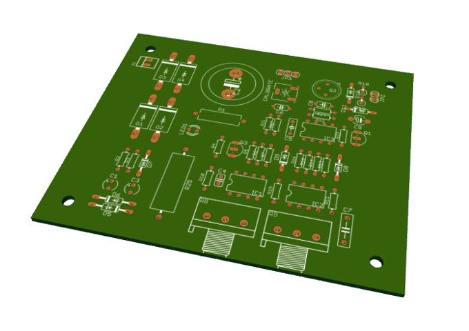
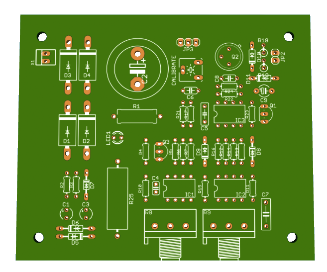
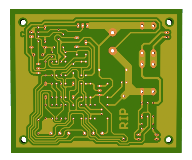
Schematic and PCB are designed in Eagle software and the source files are available on the links at the bottom of the page. The PCB design has connectors for 2N3055 transistor, input and output voltage. Also on-board potentiometers are added.
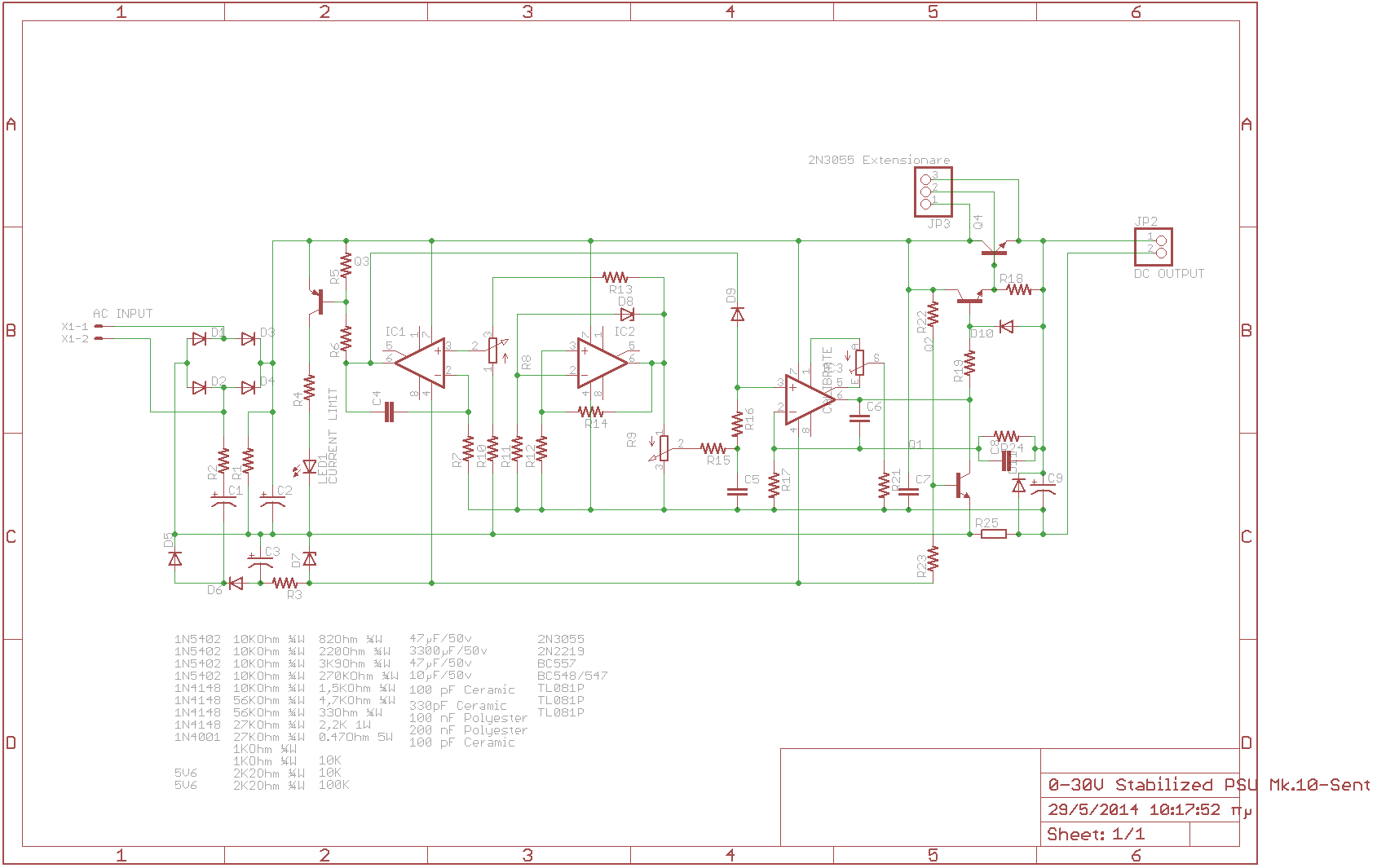
Schematic
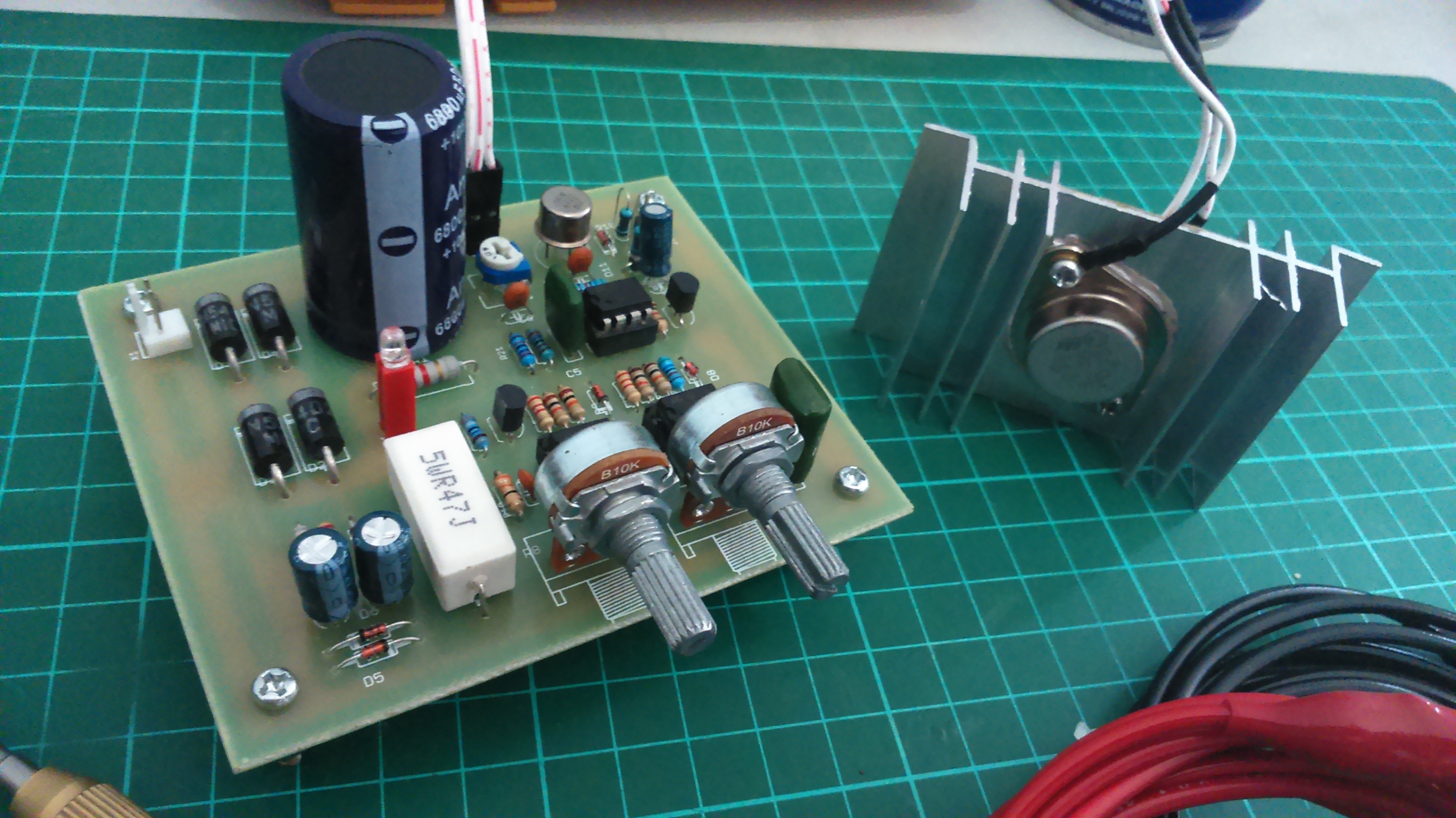
Photos
Gerber does not open.eagle drawing incorrect.please PCB PDF
What is the problem with Eagle files?
sir the dimensions shown are incorrect eg: 3300uf capacitor position is marked as c2 actually it is c1.could you provide correct layout?
Please download the Eagle design files to check for the parts list. The part list listed here has some errors
Thank you very much, okay, okay, I got
Gerber does not open.eagle drawing incorrect.please PCB PDF
Can anyone provide me proteus schematic file
and the list of parties to know the value with respect to the location
Thank you
Hi there,
What’s the PCB designing software you used in designing this board?
thanks
It’s designed on Cadsoft Eagle and PCB files are rendered on http://mayhewlabs.com/3dpcb
Sir
Required power supply kit please send price
We are sorry, we don’t sell kits.
Excellent webpage with very good photos and design too.
Does this modified circuit is working?? Still no part’s list
how can get it ??? anyone ??
Hi friend, this power supply has short-circuit protection?
best regards.
This PSU has output current regulation so the current can’t be more than the specified one
Please define design of parts.for example what is the amount of R1,R6,R14,R17…..??
Please download the Eagle files and open them, then click on the components values to see each part’s value.
A B C D E F G H I
id value quantit package componen
y ts
1 1N5402 4 DO201-15 D1 D2 D3 D4
2 1N4148 2 DO35-10 D5 D6 3 2 2K 1W 1 P061315 R1
4 82Ohm 1 2047 R2
录W
5 47碌F5 2 TT2D4 C1 C3
0v
6 3300碌 1 EB20D C2
F50v
7 220Ohm 1 2047 R3
录W
8 5V6 2 DO34Z7 D7 D8
9 BC54854 1 TO92-EBC Q1
7
10 2N2219 1 TO5 Q2
11 BC557* 1 TO92-EBC Q3
12 CURRENT 1 LED3MM LED1
LIMIT
13 3K9Ohm 1 2047 R4
录W
14 2K2Ohm 2 2047 R5 R16
录W
15 10KOhm 5 2047 R6 R7 R12 R14 R22
录W
16 TL081 3 DIL08 IC1 IC2 IC3
17 330pF 1 C025-024 C4
Ceramic X044
18 10K 2 3RP1610N R8 R9
19 33Ohm 1 2047 R10
录W
20 2N3055 1 TO3A Q4
21 4 7KOhm 1 2047 R11
录W
22 56KOhm 2 2047 R13 R24
录W
23 27KOhm 2 2047 R15 R17
录W
24 100 nF 1 C050-025 C5
Polyest X075
er
25 1N4148 2 DO35-7 D9 D10 26 1KOhm 2 02072V R18 R19
录W
27 100 pF 2 C050-024 C6 C8
Ceramic X044
28 100K 1 CA6V CALIBRAT
E
29 270KOhm 1 2047 R21
录W
30 200 nF 1 C075-032 C7
Polyest X103
er
31 1 5KOhm 1 2047 R23
录W
32 10碌F5 1 E5-4 C9
0v
33 0.47Ohm 1 VTA54 R25
5W
34 1N4001 1 DO35-7 D11 35 DC 1 1X02 JP2
OUTPUT
36 2N3055 1 1X03 JP3
Extensi
onare
37 AC 1 22-23-20 X1
INPUT 21
Sir from where did you these values..could you provide the source please
Hi there!
Is it possible to use 12VAC as input voltage as well or do I have to change all the values of the components?
Best regards!
Can any one plzz send me the snapshot of part list .
I haven’t eagle
1. You can buy a chinese kit which is exact copy of this project on ebay !
2. One reader warned about exceeding the AMR of the TL081 op-amps and suggested regulating the positive voltage for them to 29V. This will limit the output voltage to 29 – 2*Vbe. To overcome this one can use a LT1007 from Linear Technology (AMR=44V V- to V+ ) for the last op-amp and feed it from the unregulated positive rail.However the output zeroing arrangement will be different.
It will be simpler if you use ic 723. It has a 7.2 volts reference voltage. You can connect any npn transistor and 2N3055 power trasistor. Only precaution is that adujust base resistor to keep transistor in linear region i.e. do not allow them to go in to saturation. Ihad made 100s of them in 1972 i.esome 45 years ago. You canalso do the same thing with 7805 3A voltage regulator whose common pin is connected to output of op amp. The op will be a voltage follower mode. The input is given by a simple potentiometer.
Sir, can I know the AC Input values. is it 240V AC? or you need a transformer secondary as input.
How I can display on front panel a value of current limit? Any ideas?
you can buy a amp/volt meter on Ebay nealy 2$
Hello everybody
I have a few questions
What is the components value.
example R1 value ? or R2 value ???
Thank you all
I found it
R1 = 2,2 KOhm 1W
R2 = 82 Ohm 1/4W
R3 = 220 Ohm 1/4W
R4 = 4,7 KOhm 1/4W
R5, R6, R13, R20, R21 = 10 KOhm 1/4W
R7 = 0,47 Ohm 5W
R8, R11 = 27 KOhm 1/4W
R9, R19 = 2,2 KOhm 1/4W
R10 = 270 KOhm 1/4W
R12, R18 = 56KOhm 1/4W
R14 = 1,5 KOhm 1/4W
R15, R16 = 1 KOhm 1/4W
R17 = 33 Ohm 1/4W
R22 = 3,9 KOhm 1/4W
RV1 = 100K trimmer
P1, P2 = 10KOhm linear pontesiometer
C1 = 3300 uF/50V electrolytic
C2, C3 = 47uF/50V electrolytic
C4 = 100nF polyester
C5 = 200nF polyester
C6 = 100pF ceramic
C7 = 10uF/50V electrolytic
C8 = 330pF ceramic
C9 = 100pF ceramic
D1, D2, D3, D4 = 1N5402,3,4 diode 2A – RAX GI837U
D5, D6 = 1N4148
D7, D8 = 5,6V Zener
D9, D10 = 1N4148
D11 = 1N4001 diode 1A
Q1 = BC548, NPN transistor or BC547
Q2 = 2N2219 NPN transistor
Q3 = BC557, PNP transistor or BC327
Q4 = 2N3055 NPN power transistor
U1, U2, U3 = TL081, operational amplifier
D12 = LED diode
Wrong, it is an old revision. In the new part numbers do not match.
Excellent webpage with very good photos and design too.
Does this modified circuit is working?? Still no part’s list
how can get it ??? anyone ??
In the new part numbers do not match.
Could someone please put the list of components and their respective number in the PCB? Thank you!
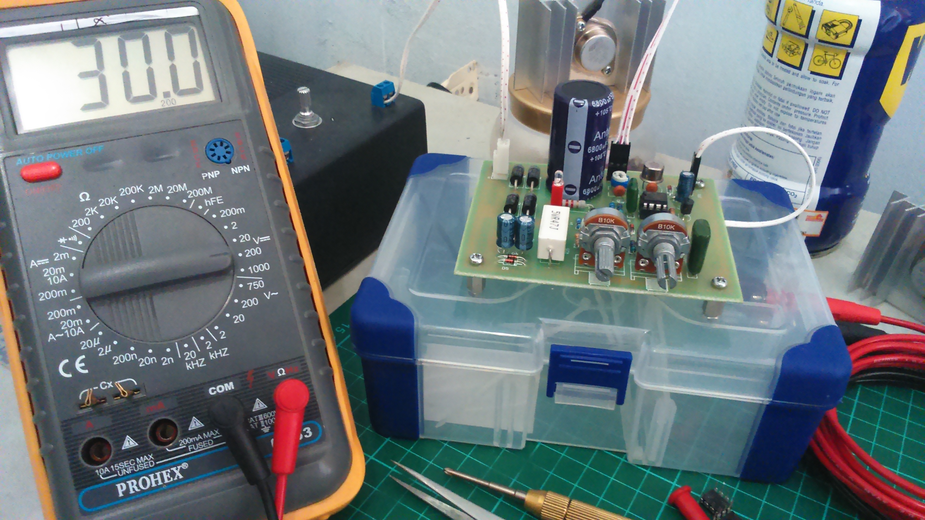
I built it
I use AC 24v transformer and i can measure voltage on filter cap 33v dc , all TL081 very very hot
TL081 using maximum 30v
somethings wrong
final situation
parts are correct
but still does not work 🙂
Part Value
C1 47µF/50v
C2 3300µF/50v
C3 47µF/50v
C4 330pF Ceramic
C5 100 nF Polyester
C6 100 pF Ceramic
C7 200 nF Polyester
C8 100 pF Ceramic
C9 10µF/50v
Calibrate 100K Trimmer
D1 1N5402
D2 1N5402
D3 1N5402
D4 1N5402
D5 1N4148
D6 1N4148
D7 5V6 Zener Diode
D8 5V6 Zener Diode
D9 1N4148
D10 1N4148
D11 1N4001
IC1 TL081P
IC2 TL081P
IC3 TL081P
JP2 DC OUTPUT
JP3 2N3055 Extensionare
LED1 CURRENT LIMIT LED 3mm
Q1 BC548/547
Q2 2N2219
Q3 BC557
Q4 2N3055
R1 2,2K 1W
R2 82Ohm ¼W
R3 220Ohm ¼W
R4 3K9Ohm ¼W
R5 2K2Ohm ¼W
R6 10KOhm ¼W
R7 10KOhm ¼W
R8 10K Potentiometer
R9 10K Potentiometer
R10 33Ohm ¼W
R11 4,7KOhm ¼W
R12 10KOhm ¼W
R13 56KOhm ¼W
R14 10KOhm ¼W
R15 27KOhm ¼W
R16 2K2Ohm ¼W
R17 27KOhm ¼W
R18 1KOhm ¼W
R19 1KOhm ¼W
R21 270KOhm ¼W
R22 10KOhm ¼W
R23 1,5KOhm ¼W
R24 56KOhm ¼W
R25 0.47Ohm 5W
X1 AC INPUT
The only thing I know is that the C1 is 3300uF it is the filter capacitor . With this error I suspect that other components can also be wrong. Owner of this project, please help us !!!!
It is a filter capacitor, I used 6800uF instead, higher value caps helps eliminate ripple provided with correct voltage rating , don’t hesitate to play a little bit upgrading the value of this cap, since we never knew the output quality of the transformer used, one could find a very unpleasant step-downed output due to electrical disturbance, that is, some sufficient filtering procedure needed to eliminate the ripple
Resistor R16 pcb connection short cut pcb parth
Has anyone found an alternative to the TL082 as 33.9 volts is a little close to the chips max supply for comfort… not to mention some manufacturers quote a max supply of 30 volts (+/- 15)…
Hello
watch the video
same project but chinese version
same ic TL081 different zener diode 5.1v
This is a new copy of the original unreliable project. It has the parts list all messed up and it has a new pcb with some high current traces too thin. Many of its parts are overloaded. If a 24VAC transformer is used and it produces 25V when this project has no load then the TL081 opamps have a total supply of 39.6V (positive 34V plus negative 5.6V) but 36V is their maximum allowed voltage. I could not find what is the transformer in this copy but it was 24CAC/3A in the original which has a voltage too low for this circuit to produce 30V at 3A and this little transformer will be overloaded since it must pass 35.3V x 3A= 105.9VA instead of 24V x 3A= 72VA which is too low.
There are long threads in the forum where we fixed its errors by using 44V opamps, a newer more powerful driver transistor, additional output transistors each with current-sharing emitter resistors, many larger resistors for them to survive the heat, a much larger main filter capacitor and a higher voltage and higher current transformer. A few pcb designs have been made. The improved version works very well and is reliable.
can you give the link to the latest version with all of the updates that you mentioned?
id value quantity package components
1 1N5402 4 DO201-15 D1,D2,D3,D4
2 1N4148 2 DO35-10 D5,D6
3 2,2K 1W 1 P061315 R1
4 82Ohm 录W 1 02047 R2
5 47碌F50v 2 TT2D4 C1,C3
6 3300碌F50v 1 EB20D C2
7 220Ohm 录W 1 02047 R3
8 5V6 2 DO34Z7 D7,D8
9 BC548547 1 TO92-EBC Q1
10 2N2219 1 TO5 Q2
11 BC557* 1 TO92-EBC Q3
12 CURRENT LIMIT 1 LED3MM LED1
13 3K9Ohm 录W 1 02047 R4
14 2K2Ohm 录W 2 02047 R5,R16
15 10KOhm 录W 5 02047 R6,R7,R12,R14,R22
16 TL081 3 DIL08 IC1,IC2,IC3
17 330pF Ceramic 1 C025-024X044 C4
18 10K 2 3RP1610N R8,R9
19 33Ohm 录W 1 02047 R10
20 2N3055 1 TO3A Q4
21 4,7KOhm 录W 1 02047 R11
22 56KOhm 录W 2 02047 R13,R24
23 27KOhm 录W 2 02047 R15,R17
24 100 nF Polyester 1 C050-025X075 C5
25 1N4148 2 DO35-7 D9,D10
26 1KOhm 录W 2 02072V R18,R19
27 100 pF Ceramic 2 C050-024X044 C6,C8
28 100K 1 CA6V CALIBRATE
29 270KOhm 录W 1 02047 R21
30 200 nF Polyester 1 C075-032X103 C7
31 1,5KOhm 录W 1 02047 R23
32 10碌F50v 1 E5-4 C9
33 0.47Ohm 5W 1 VTA54 R25
34 1N4001 1 DO35-7 D11
35 DC OUTPUT 1 1X02 JP2
36 2N3055 Extensionare 1 1X03 JP3
37 AC INPUT 1 22-23-2021 X1
and finaly it works
now problem output is max 24v 1,6 amp
can you help me with the list of components in order to implement it as it can work and please reply as soon as you can
https://www.electronics-lab.com/project/0-30-vdc-stabilized-power-supply-with-current-control-0-002-3-a/ you can find correct part this site
and also you have to disconnect R16 short on pcb
Caution! This PCB is poorly designed. Look at the scheme for R25-shunt resistance. On the left side is bonded directly to the rectifier bridge, on the right to the output terminal of 0V. This connection can be loaded with a maximum output current of 3A. Now find this connection on the PCB and look at how thin it is and how it runs. Connection is done very wrong. Use ticker wire and connect it to bottom pin of R25, other end of wire connect to output pin 0V_GND. Second tick wire connect on Emitter of 2N3055 and other end on positive output pin. This is it, hope it help’s to someone. Use tick wires also from AC input to bridge (D1-D4).
Tick and Ticker shoud be “thick” and “thicker”. Sorry 🙂
I don’t trust this power supply and the circuit i have build ed this power supply 2 x in the past and what i have found was that the Voltage adjustment worked fine adjusting from 0V – 30V but when you use the Current limiter over 2 amps it blows the output transistor 2N3055 every single time and yes before somebody asks I did use a very big heat sink to no avail so i would rather the say the amps rating for this power supply is 2 Amps and not 3 Amps as Stated
I do not know why the unreliable original project was replaced by this copy that has the same problems and added more problems instead of using the version that we fixed in the forum.
What is the link to the forum where this power supply’s where fixed as there seems to be so many forums about this project it’s not even funny maybe Electronics Lab is jus continuelly putting up this faulty power supply just to generate traffic thru their webpage to keep some paying advertisers happy please supplycthe correct midified circuit as well as the correct modified pcb and the correct transformer specs and part specs if you are unable to do so please remove this stupid aeticle of a power supply which doesent work as promised at stip fooling people in wasting their money and time in this not well thought thru project. I wasted a lit of money time and effort building this fake and error ridden circuit i would have been better off buying a power supply in a shop
There is a topic here: https://electronics-lab.com/community/index.php?/topic/40835-0-30v-0-3a-latest-data/ trying to summarize the fixes of this power supply.
Yet another observation :). Look on ground pin 4 of IC”.Why it is connected to right side of R25 (shent)? There is happening a voltage drop of output current. That voltage drop is info for calculating and comparing of that current and not for powering off IC2. So, R11,R12,4-IC2,R9,C5,R17 and C7 should be connected to real ground coming from C2 (left side R25). BTW R21 and upper trimmer has no point here. I didnt build any of this PS. If I will, I will buy one from Banggood and rearrange it. Actually that PS is that bad, it is just old design and fully good for home lab.
Meaned IC2…