Pull-up Resistors
Pull-up Resistors Pull-up resistors are used to avoid self-biasing or floating digital inputs. The pull-up resistor connects the digital input to the correct biasing level and eliminates the uncertainty caused by a floating input.
Pull-up Resistors
Pull-up resistors are used to avoid self-biasing or floating digital inputs. The pull-up resistor connects the digital input to the correct biasing level and eliminates the uncertainty caused by a floating input. A floating input creates a no input condition and may cause random biasing leading to incorrect logic or decision.
A logic gate is a basic building block of a digital circuit and they constitute complex Integrated Circuits (IC’s) and microcontrollers etc. having multiple inputs and outputs connected to external circuitry. These logic inputs and outputs can have only two states that are “0” and “1” or “LOW” and “HIGH”, respectively. These logic states represent two different voltage levels such as a logic “0” by a 0 Volts and logic “1” by a +5 Volts. These logic states are differentiated by different voltage levels or ranges depending upon the type of logic family. Any voltage below a certain level may lead to a “0” state and, on the other hand, any voltage above a certain level may lead to a “1” state.
The digital logic circuits make decisions based on only these two states and a voltage outside of differentiable logic levels could lead to uncertainty and the state of logic “0” or “1” cannot be sensed correctly. Such a condition could falsely trigger a digital circuit or logic gate.
Consider the following digital circuit, the recognizable voltage states for this digital gate are 0V and +5V for logic “LOW” and “HIGH”, respectively. The “X” & “Y” inputs of the digital circuit are connected to the ground (0V) through respective switches namely “a” &”‘b”. When the switch “a” is in close (ON) position then input “X” is connected to ground (0V) which is the correct voltage stage for logic “LOW”. Similarly, the closing of the switch “b” leads to the “LOW” logic state as well.
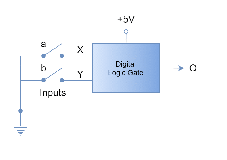
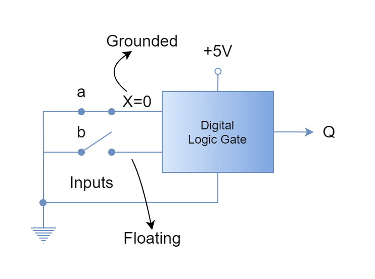
However, when switch ‘a’ is open (OFF) then there is no voltage connected to the input “X” and an expected state would be a logic “HIGH”. But for achieving a logic “HIGH”, the input needs to be connected to +5V which does not seem to be a case here. The input “X” is said to be in the floating condition as it is not effectively connected to any voltage level. Apparently, such a condition may cause input “X” to a have “LOW” logic state but expectations were to have a “HIGH” logic state. Consequently, leading to a false decision at the output “Q”. Moreover, such a floating input is prone to the slightest interferences, and noises could make input change state. The worst could be leading to random shifting of states or oscillation.
The uncertainty, false-triggering, or oscillation in digital circuits due to floating or unused inputs can be prevented by connecting them to a certain voltage level appropriate to the circuit. The tying of inputs defines the logic states in different controlling states of inputs such as seen above in the open switch state where it was unused. In digital circuits, many digital gates or their inputs remain unused and require tying up or down using pull-up or pull-down, respectively. A number of unused inputs prescribing to the same logic state or condition can be tied together using a single pull-up or down resistor.
A pull-up resistor is used to connect an input of the “AND” or “NAND” gate to VCC. Whereas, a pull-down resistor is used to connect the input of the “OR” or ”NOR” gate to the Ground.
Why Pull-up Resistor?
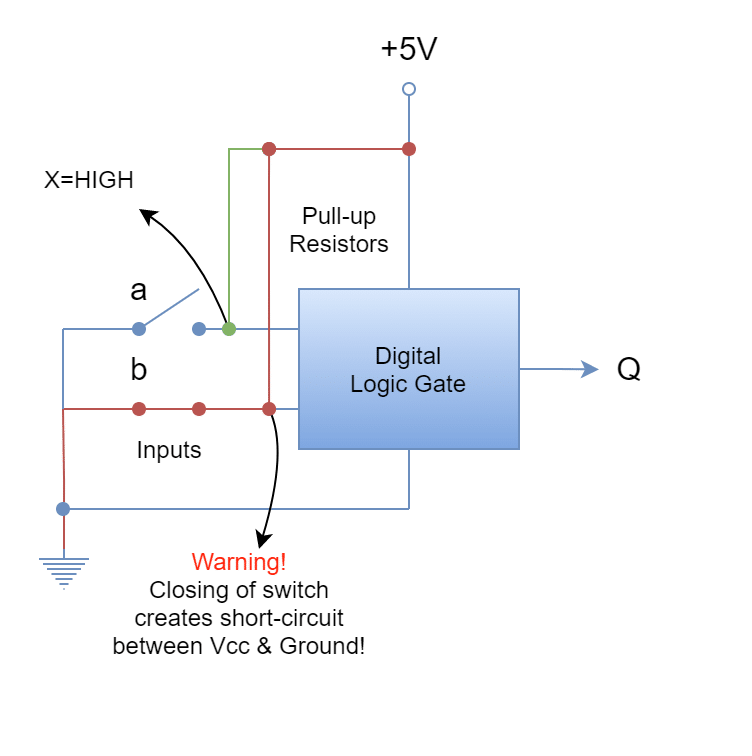
Consider the following diagram of a two-switches case wherein instead of a floating state a second state is achieved by connecting inputs to +5V (a logic “HIGH” voltage level). Now, when switches are open, a logic “HIGH” state is present at the inputs. However, the closing of any switch would short-circuit the +5V with the Ground (0V) and causing an excessive current to flow. This could fry up the digital gate, input, and/ or circuity if there is no short-circuit protection is present. Instead, a pull-up resistor can be used between input and +5V to overcome this issue. The value of the pull-up resistor should be selected in such a way that when pulled-up allows a sufficient voltage drop to bring input voltage to logic “0”.
Pull-up Resistor Application
In the following figure, a suitable pull-up resistor is used to pull up each input of the digital circuit. When any of the switches are open (OFF) then the respective input is connected to +5V via this pull-up resistor. The current flowing into the input is very small and, as such, causes a negligible voltage drop across the pull-up resistor. Eventually, a full +5V (nearly) gets applied at the input to bring the logic “HIGH” condition.
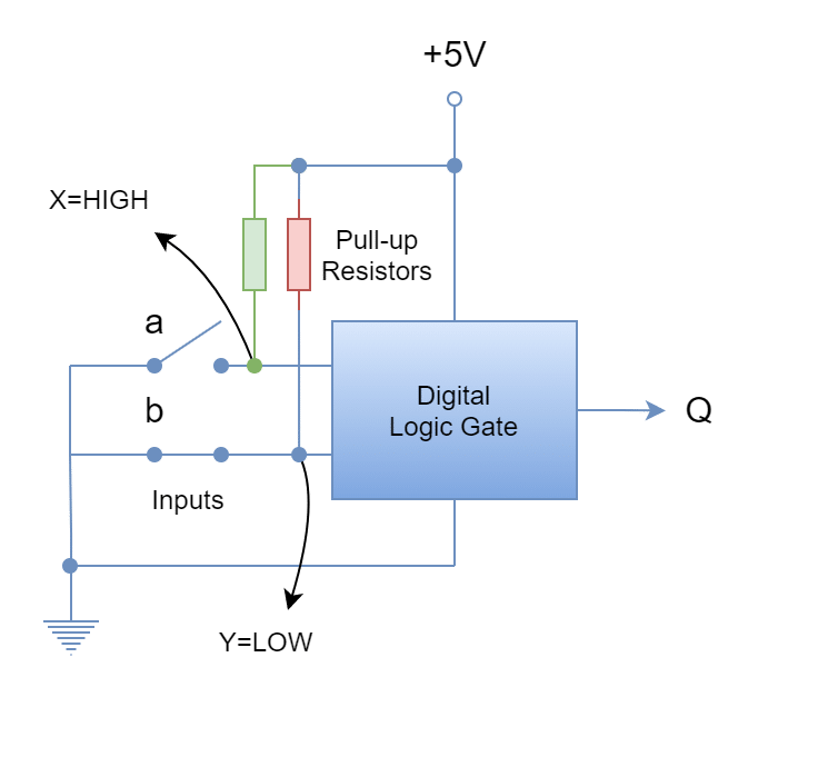
Upon closing of any switch, the input is effectively connected to ground (0V) and a firm logic “LOW” condition is sensed by the logic gate/ circuit. However, this time, the VCC and Ground are not shorted due to the insertion of a pull-up resistor and a very little current flow through it. Now, both logic “HIGH” and “LOW” states are effectively achieved in the digital circuit using pull-up resistors. The output (Q) of the digital circuit will reflect the true picture of input states which was initially misleading due to floating inputs.
Calculation of Pull-up Resistor Value
As discussed in previous articles, the logic gates are characterized not only by the operating voltage but also by their current sinking and sourcing capabilities. Besides the two distinct voltage states presenting logic states “0” & “1”, there are maximum and minimum voltages defining voltage ranges for each state. In the following diagram, the voltage ranges for logic “HIGH” and “LOW” states are shown which are separated by an intermediate state.
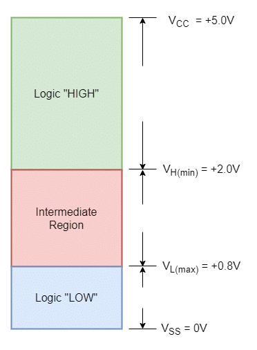
It is obvious from the figure that the input needs to have at least 2V to be considered as a logic “HIGH” and, on the other hand, an input should remain below (maximum) a 0.8V to be sensed as a logic “LOW”. In short for a TTL 74LS family, the logic “HIGH” state ranges from 2.0V to 5.0V and the logic “LOW” state from 0.8V to 0V.
The current flow between input and output of logic gates is dependent on the input logic level i.e. “0” or “1”. The logic “0” level makes the input as current-source as the current flows from input to logic “LOW”. Whereas, a logic “1” makes the input as current-sink and the current now flows towards the input from logic “HIGH”. When an input is at logic “HIGH” then the input acts as a ground and the current flow is considered positive (TTL74LS series have a typical value of 20uA). Likewise, at the logic “LOW” state, the current flows out of the TTL input and is considered negative having a value of -400uA for the TTL74S logic series.
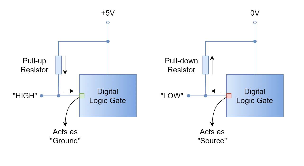
When an input is pulled high it acts as a current sink and positive current flows into it. The TTL74S logic series has a rated positive current of 20uA and a minimum voltage threshold for a logic “1” of 2.0V. In the calculation of the pull-up resistor, the minimum voltage threshold is used to remain on the safest side.
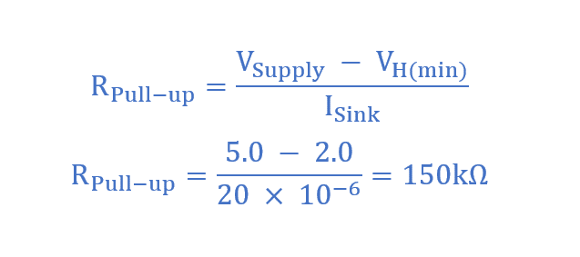
The resistance value obtained above is the maximum value which will ensure a maximum voltage drop of 3V at a minimum 20uA sink current. The voltage is usually kept close to the upper limit of voltage (close to +5V) and this is done by reducing the pull-up resistance value. However, such a close margin can be easily overcome due to resistance tolerance or change in supply voltage, etc. Moreover, the power dissipation is more in low-value pull-up resistance due to an increase in current which should be avoided in any case. The suitable resistance value for a pull-up resistance ranges from 10kΩ to 100kΩ.
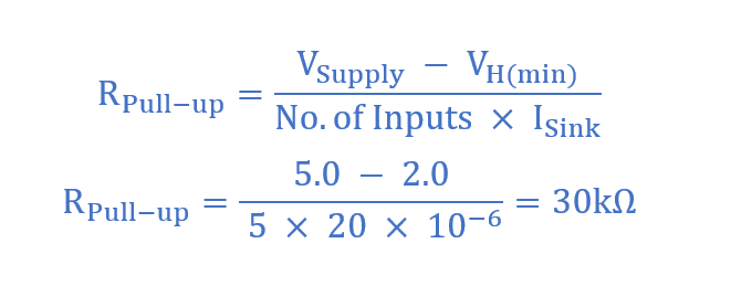
In a similar way, a number of inputs can be tied together using a single pull-up resistance rather than using pull-up resistance at each input, separately. In such a case, the current flowing through single pull-up resistance will number of inputs times the minimum positive (sink) current. In the following calculation, a pull-up resistance value is determined through which five inputs will be pulled up.
Pull-down Resistors
Just like a pull-up resistor, the pull-down resistor ties the input with an effective voltage level. However, contrary to a pull-up resistor, a pull-down resistor connects the input of a logic gate with the Ground (0V) or logic “0” state. The input becomes a current source and supplies current through a pull-down resistor towards the ground. The resistive value of a pull-down resistor for a TTL logic gate is more critical compared to the one used with a similar CMOS gate. It is because of TTL’s high current sourcing capability when its input is in a “LOW” state. The value of the pull-down resistor can be calculated in a similar fashion described above for a pull-up resistor. The TTL 74LS logic series requires a maximum of 0.8V in order to sense it as logic “0” and can deliver a minimum source current of 400uA. The pull-down resistor can be calculated using these parameters as follow:
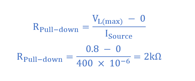
This is the maximum pull-down resistor which ensures that voltage drop would be sufficient enough at the input to be sensed as logic “LOW”. Further increase in the pull-down resistor value will increase the voltage drop across the resistor and a voltage above 0.8V would be sensed as a logic “HIGH”. The good practice is to keep at least a 0.4V drop across the pull-down resistor.
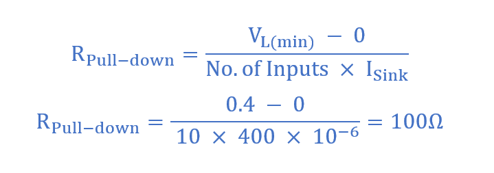
A number of unused inputs can be connected together with a single pull-down resistor. A sample calculation for a fan-in of 10 is shown below:
The input can be pulled down without using a resistor but is often avoided to avoid excessive current flow or power loss. The pull-down resistor limits the source current flowing towards the ground.
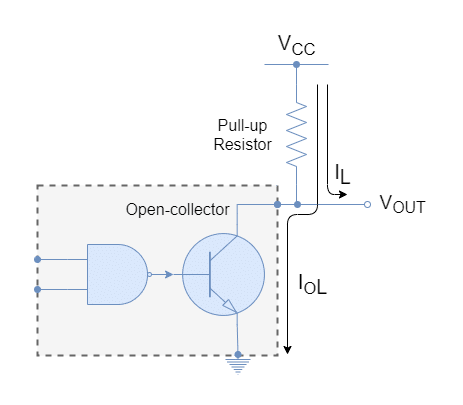
Open-collector Outputs
The outputs of the logic gates are connected with other logic gates which may belong to the same or different logic family. If the output is connected to the same logic family such as TTL to TTL or CMOS to CMOS etc. then logic voltage levels match to produce a coherent result. However, when a connection between two different logic families is required or a load is to be connected to a different voltage level then a logic gate with open-collector output is used. The logic gates are manufactured with the open-collector circuitry at the output of the logic gate. The open-collector output is then derived from desired voltage level using a pull-up resistor. In contrary to the aforementioned pull-up or pull-down which were connected to the logic gate’s input, this pull-up is connected to the output of a logic gate. The term open-collector is used for TTL devices whereas open-drain for CMOS devices.
The open-collector or open-drain outputs are mostly used in inverters, drivers, or buffers where the output is connected to a different voltage level or to deliver high output current which may not be possible using normal logic outputs. For example, driving high current LEDs, relays, DC and servo motors, etc.
In the following figure, the open-collector output of a TTL 74LS01 is shown. In the absence of a pull-up resistor, it is eminent that the output of the logic gate will be either be connected to the ground when “HIGH” or floating when “LOW”. In order to avoid a floating condition, it is necessary to use a pull-up resistor at the output of an open-collector output. The pull-up resistor pulls the output to “HIGH” when the transistor is “OFF” and, upon switching to “ON”, the output becomes “LOW”.
Calculation of Open-Collector Pull-up Resistor Value
The value of the open-collector pull-up resistor depends upon the load which is driven through it and the current-sinking capability of the open-collector (transistor). When the transistor is in an “ON” state then current flows through the transistor and the value of the pull-up resistor must not exceed the current handling rating of the transistor. On the other hand, the load is supplied through this pull-up resistor when the transistor is in the “OFF” state. In this state, the pull-up resistor value should allow the required load current.
The output voltage levels are required to remain under permissible limits in order to be recognized as logic “LOW” or “HIGH”. For TTL 74LS logic family devices, the minimum “HIGH” logic voltage is 2.7V and the maximum “LOW” logic voltage is 0.5V. In short, the outputs of TTL 74LS devices are considered as logic “LOW” within 0 to 0.5 Volts and as logic “HIGH” within 2.7 to 5.0 Volts.
Consider the following calculation as an example for TTL NAND open-collector (74LS01):
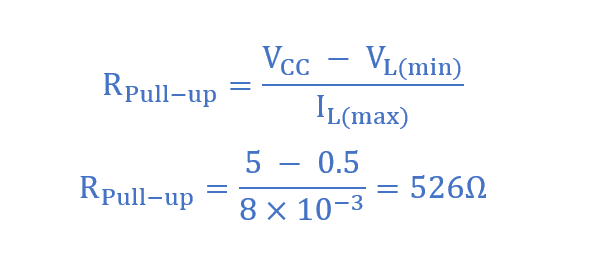
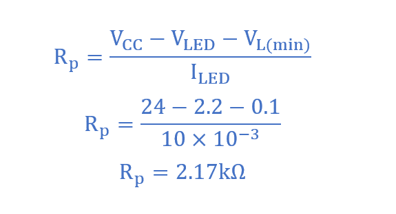
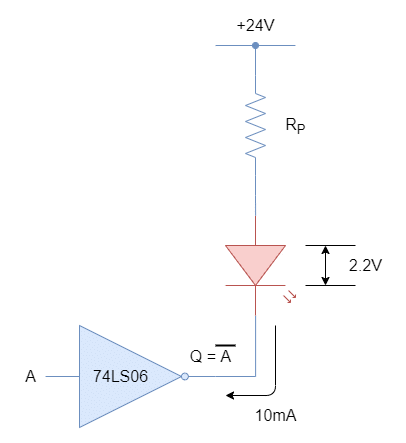
This is the minimum resistance required to limit the current to 8mA which is the maximum current at the logic “LOW” state. In a similar way, the pull-up resistor value can be calculated through which an external load is connected. The external load usually requires high voltage or current and, for this purpose, normally hex inverter buffers are used. The TTL 74LS06 Hex Inverter Buffer uses 5V for biasing but its open-collector can support up to 30 Volts and a maximum of 40mA current at logic “LOW” level.
In the following example, a LED is driven from a 24 Volt supply using a 74LS06 Hex Inverter Buffer. The LED requires 10mA current at a 2.2V voltage drop. The 74LS06 Hex Buffer requires at least 0.1V at the input to sense the “LOW” state. The current limiting resistor value:
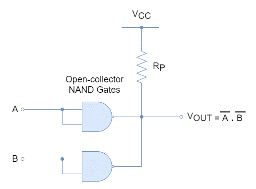
Wired AND Logic
The open-collector outputs can be connected together through a single pull-up resistor. These open-collector outputs tied together forms the Wired AND logic because the outputs are AND’ed together just like they were connected to an AND gate.
Conclusion
- The open-circuits/ floating inputs of digital logic gates may get self-bias leading to false triggering, random switching, or oscillation about logic states.
- The pull-up or pull-down resistance is used to tie up a floating input to an effective logic level voltage.
- The pull-up resistance ties up the inputs of AND and NAND gates with logic “HIGH” voltage.
- The pull-down resistance ties the inputs of OR and NOR gates with the logic “LOW” voltage.
- The logic states of “HIGH” and “LOW” levels are distinguished by two different voltage levels. For example, the TTL 74LS series used Ground (0) voltage as logic “LOW” and +5V as logic “HIGH” level.
- Besides two distinctive voltages states, there are ranges of voltages that contribute to deciding logic levels. Like, TTL 74LHS Series, has a range from 0 to 0.8V for logic “LOW” and from 2.8 to 5.0V for logic “HIGH”.
- The pull-up or down resistance value depends on the logic state of the input. At logic “LOW”, the input becomes a source (positive current) and a sink (negative current), otherwise (logic “HIGH).
- The value of pull-down resistance is more critical compared to pull-up resistance because of low input voltage and high current.
- The pull-up resistance usually ranges from 1kΩ to 100kΩ and mostly 10kΩ resistance is used in digital circuits. Whereas, the pull-down resistance ranges from 50Ω to 1kΩ.
- The pull-up resistances are also used in conjunction with open open-collector (TTL) or open-drain (CMOS) outputs to drive outputs to desired logic voltage.
- The open-collector or open-drain outputs are also used for loads requiring high currents such as relays, DC motors or LEDs, etc.
- Multiple open-collector outputs connected together through an external pull-up resistance forms a Wired AND Logic.


