Dual-Channel Synchronous Rectification Controller Tackles LLC Applications
Diodes Incorporated’s APR3492 is a new MOSFET driver for LLC resonant converters that features forward voltage regulation, fast turn-off, and a configurable light-load mode.
Diodes Incorporated has introduced the APR3492, a dual-channel secondary-side MOSFET driver for synchronous rectification in LLC resonant converters. Packaged in a standard SO-8, the device targets server and PC power supplies, notebook adapters, and LCD/LED TV applications where efficiency across a range of load conditions is a key design concern.
Diodes’ APR3492, available in a SO-8 (standard) package. Image used courtesy of Diodes Incorporated
The APR3492 Synchronous Rectification Controller
The APR3492 dual-channel MOSFET driver monitors the drain-source voltage of each SR channel in real time. When secondary-side current begins flowing through the body diode, and VDS falls below the −200 mV turn-on threshold, the IC drives the corresponding DRISR output after a 100 ns (typ.) turn-on delay, transferring conduction from the body diode to the MOSFET.
To guard against false turn-off events caused by parasitic ringing on the drain-source voltage immediately after switch-on, the APR3492 enforces a minimum on-time of 1.1 μs. During this window, the normal 30 mV turn-off threshold is masked; a secondary 100 mV threshold remains active to ensure the channel can still be turned off under abnormal conditions.
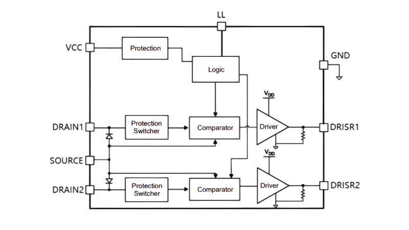
Functional block diagram of the APR3492. Image used courtesy of Diodes Incorporated
Forward Voltage Regulation and Fast Turn-Off
A notable feature of the APR3492 is its forward voltage regulation function. As the secondary-side current decreases toward the end of each conduction interval, the drain-source voltage drop decreases accordingly. Once VDS reaches the −45 mV VON_REG level, the IC begins sinking current from the DRISR pin, gradually reducing the gate drive voltage. This increases the MOSFET’s RDS(ON) and maintains VDS at approximately −45 mV.
The practical effect is that the gate voltage is already at a low level by the time the 30 mV turn-off threshold is reached, meaning there is less gate charge to remove and the MOSFET switches off more quickly. The turn-off propagation delay is specified at 70 ns (typ.), with a maximum of 90 ns.
Once a channel turns off, a 0.4 μs turn-off blanking window prevents re-triggering from residual drain-node noise. An anti-cross-conduction function also keeps one channel’s drive signal inactive until the opposite channel fully turns off.
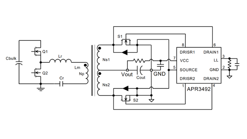
Typical applications circuit of the APR3492. Image used courtesy of Diodes Incorporated
Light Load and Smart Blanking
At light loads, the SR MOSFET on-time shortens. If the measured on-time stays below the configurable tLL_EN threshold for 1 ms, the APR3492 enters light-load mode and latches off the drive signals entirely. The quiescent current then drops to a typical 175 μA. The IC continues monitoring the body diode on-time and resumes normal SR operation as soon as it exceeds the tLL_EX exit threshold. The tLL_EN entry threshold is set via an external resistor, allowing designers to control where the transition occurs.
The device also includes a smart blanking function to handle burst and skip modes used by some LLC controllers at light load. If the interval between two consecutive DRISR1 falling edges is shorter than 3.5 μs, subsequent drive signals are suppressed for 10 μs to inhibit false SR turn-on during LC oscillation periods.


