
IBM Unveils Sub-1 Nanometer Chip With New Nanostack Architecture
A new three-dimensional transistor design pushes logic scaling past the 1-nm barrier, promising sizable gains in speed and efficiency.
IBM has introduced a transistor architecture that extends logic scaling below the 1-nanometer node, a threshold long treated as a practical limit for silicon processing. The new design, called nanostack, produced a chip built at the 0.7-nm, or 7-angstrom, node that packs nearly 100 billion transistors onto a die roughly the size of a fingernail—almost double the density of the 2-nm chip IBM introduced in 2021. Published results project the chip could deliver up to 50 percent more performance or 70 percent greater energy efficiency compared with IBM’s 2-nm node, gains aimed at workloads spanning generative AI, cloud infrastructure, and next-generation electronic devices.
A Three-Dimensional Departure From Nanosheet Design
Nanostack extends nanosheet technology, IBM’s current leading-edge architecture, into a third dimension. Rather than placing transistors side by side on a single plane, the design vertically stacks and staggers them, relying on 3D sequential integration to fit more transistors into the same footprint. Each stacked layer can also draw on a different combination of materials, letting engineers tune the performance and power characteristics of individual transistors independently rather than treating the whole die as a single optimization target.
Confirming the Architecture Works
IBM validated the nanostack approach through several experiments, including ultra-thin dielectric bonding during CMOS integration, the demonstration of dual-channel engineering, and the operation of a functional CMOS inverter with expected switching performance. Together, the results indicate the architecture is physically manufacturable and capable of supporting real computation, not just serving as a theoretical construct. Separately, research presented at VLSI 2026 showed the nanostack structure enabling 40 percent scaling in SRAM, a result that points toward denser on-chip memory for data-hungry AI accelerators.
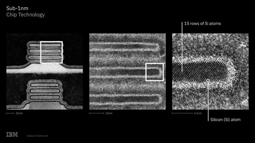
IBM’s nanostack architecture at three magnifications, culminating in a resolved lattice showing individual silicon atoms. Image used courtesy of IBM
A Manufacturing Path Rooted in Albany
IBM and its partners are developing the technology at a semiconductor research facility in Albany, New York, which will soon house a High Numerical Aperture Extreme Ultraviolet (High NA EUV) lithography tool built by ASML for ultra-precise circuit printing. Lam Research, Tokyo Electron, and SCREEN Semiconductor Solutions have worked alongside IBM to refine High NA EUV processes and tools, a collaboration that has already produced functional devices. IBM expects nanostack to reach production within roughly five years and views the architecture as the basis for at least another decade of scaling.
Taken together, nanostack marks one of the more substantial structural shifts in transistor design in recent memory, moving the industry from stacking materials to stacking entire devices. Engineers working on data center silicon, AI accelerators, and power-conscious embedded systems have reason to watch how this architecture matures, since the promised density and efficiency gains could ripple into everything from cloud servers to the next generation of edge hardware. It’s still early, with production still being years away, but the underlying physics appears sound, and that alone makes nanostack worth following as the sub-1-nm era gets underway.


