Onsemi Develops Vertical Gallium Nitride Power Semiconductor Technology
The vertical gallium nitride (vGaN) semiconductors vertically conduct current through the chip, enabling higher operating voltages, faster switching, and reduced energy loss compared to traditional silicon.
The global demand for high-efficiency power conversion is rapidly increasing, driven by the expansion of AI data centers and the increasing electrification of vehicles. While silicon carbide and first-generation gallium nitride (GaN) devices (primarily lateral GaN) have offered significant improvements over traditional silicon, they still present limitations in scalability for ultra-high voltage and high-power density applications.
Traditional, commercially available GaN devices are typically grown on non-GaN substrates, such as silicon or sapphire, creating a lateral structure where current flows horizontally across the chip’s surface. This structure imposes constraints on how high the device voltage can be scaled while maintaining compact size and thermal performance.
Onsemi’s new vertical GaN (vGaN) technology, built on a proprietary GaN-on-GaN substrate, fundamentally changes this architecture. By utilizing a GaN substrate, the company enables current to flow vertically through the device. This shift unlocks significant performance enhancements for the next generation of power electronics.
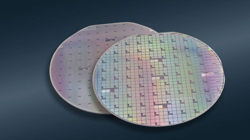
Onsemi has developed vGaN semiconductor technology that enables vertical current flow through the chip. Image used courtesy of Onsemi
Vertical Gallium Nitride (vGaN) Semiconductors
Onsemi’s vGaN technology provides critical advantages for designers, including higher voltage capability and ruggedness. The vGaN architecture is designed to handle significantly higher operating voltages in a smaller, monolithic die. The technology is now sampling in both 700 V and 1,200 V variants. This 1,200 V capability is particularly relevant for higher-voltage DC bus applications in EV charging and renewable energy systems, which exceed the typical voltage sweet spot of many lateral GaN devices. Onsemi’s vertical structure inherently offers enhanced thermal stability and robust performance under extreme electrical stress.
Another critical advantage is superior efficiency and loss reduction. The primary objective of any wide-bandgap material is to minimize energy losses during power conversion. According to Onsemi, the vGaN architecture reduces system energy losses by almost 50% compared to current-generation solutions. This massive reduction in power dissipation translates directly into lower thermal management requirements and cooling costs for the end system.
According to Onsemi, the vGaN technology reduces heat and energy loss by up to 50% compared to traditional silicon chips. Video used courtesy of Onsemi
Additionally, Onsemi’s new vGaN technology features increased power density and miniaturization. The ability to handle high voltages and switch high currents while reducing losses in a vertical structure allows for a dramatically smaller footprint. Compared to conventional lateral GaN, the vGaN devices are approximately three times smaller. This size reduction, coupled with the higher switching frequencies enabled by GaN’s inherent characteristics, significantly reduces the size of passive components like capacitors and inductors. The net result is a significant reduction in system size and weight. This density improvement is essential for packaging high-power converters into limited spaces, such as EV motor compartments or AI server racks.
Targeting AI and Electrification
The high voltage and high-frequency performance of Onsemi’s vertical GaN technology is specifically tailored to address the acute energy consumption challenges posed by emerging megatrends.
In AI data centers, for instance, AI compute systems are rapidly shifting toward higher voltage distribution, such as 800 V DC, to mitigate current and I²R losses across the rack. Onsemi’s vGaN’s 1,200 V capability and high efficiency make it an ideal fit for next-generation 800 V DC-DC converters, which require extreme power density to maximize computing power per rack unit.
For EVs, the vGaN technology enables the design of smaller, lighter, and more efficient inverters, directly contributing to increased vehicle range. In charging infrastructure, vGaN supports the development of faster, more rugged chargers with enhanced voltage handling and reduced losses.

Sampling for 700 V and 1,200 V vGaN devices is now available for early adopters. Image used courtesy of Onsemi
Advancing Semiconductor Technology
The introduction of Onsemi’s GaN-on-GaN-based vGaN technology represents a substantial leap in power semiconductor design, moving beyond the physical limitations of existing lateral GaN architectures. By conducting current vertically, the devices achieve over 1,200 V capability, superior thermal stability, and a reduction of system energy losses and size.
Onsemi’s technology provides a compelling component for designers creating ultra-efficient, high-power density systems. Key application targets include 800 V DC-DC converters in AI data centers, high-efficiency traction inverters for EVs, high-power charging infrastructure, renewable energy inverters for solar and wind, energy storage systems, and industrial automation and defense systems where size and reliability are critical constraints.


Thanks for sharing this update! Vertical GaN technology is definitely an exciting step forward for high-power and high-efficiency applications. It’s great to see advancements that can improve performance while reducing energy loss and overall system size. Looking forward to seeing how this develops and what new possibilities it unlocks in the power electronics industry.