Major Breakthrough in Chip Architecture Technology
Keeping in mind the betterment of artificial intelligence and various other CPU intensive workload, EPFL (École Polytechnique Fédérale de Lausanne) engineers have developed a new single architecture that combining logic operations and data storage. It may hold the potential to lay the fundamental work for the upcoming generation of smaller, faster, and more energy-efficient devices.
 Keeping in mind the betterment of artificial intelligence and various other CPU intensive workload, EPFL (École Polytechnique Fédérale de Lausanne) engineers have developed a new single architecture that combining logic operations and data storage. It may hold the potential to lay the fundamental work for the upcoming generation of smaller, faster, and more energy-efficient devices.
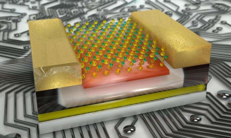
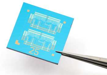
Engineers at EPFL’s Laboratory of Nanoscale Electronics and Structures (LANES) have developed these next-generation circuits that allow for smaller, faster, and more energy-efficient devices. This technology is the first to implement a 2-D material called a logic-in-memory architecture. It is a special kind of a single architecture that integrates logic operations with a memory function.
Traditionally, the energy efficiency of computer chips has been limited by the von Neumann architecture. Where data processing and data storage take place in two separate units in the Silicon. It has its drawbacks like slowing down the data transfer between the two units, wasting time and energy.
The researchers have found a way to combine these units into a single structure which significantly reduces these losses. The new EPFL chip is made from MoS2. It is a 2-D material consisting of a single layer semiconductor that’s only three atoms thick. LANES engineers had already examined the specific properties of MoS2 a few years ago, finding that it is expressly well-suited to electronics applications.
This new EPFL chip is based on floating-gate field-effect transistors or FGFETs. The benefit of these kinds of transistors is that they can hold electric charges for long periods which makes them perfect for flash memory systems for cameras, smartphones, and computers. The unique electrical proprieties of MoS2 make it particularly sensitive to charges stored in FGFETs to develop circuits that work as both memory storage units and programmable transistors. By using this wonder material MoS2, they were able to consolidate numerous processing functions into a single circuit and then change them as desired.
This ability for circuits to perform two functions is similar to how the human brain works, where neurons are involved in both storing memories and conducting mental calculations,
says Andras Kis, the head of LANES.
Our circuit design has several advantages. It can reduce the energy loss associated with transferring data between memory units and processors, cut the amount of time needed for computing operations, and shrink the amount of space required. That opens the door to devices that are smaller, more powerful, and more energy-efficient.
The team of researchers is looking forward to taking their initial research to the next level to create next-gen computing architecture technology. Which has the true potential to meet the ever-rising demand for more smart, small, and power-efficient electronic devices. More information can be found in this Nature article.


