Multi-channel Sampling Analog Comparator (MS-ACMP)
This article provides step-by-step recommendations for using the multi-channel sampling analog comparator (MS-ACMP) within the Renesas SLG47003. This project utilizes a combination of analog and digital components, creating a precise and flexible system for monitoring input signals and generating digital outputs based on specified threshold levels. The system monitors three voltage levels and detects when any of these levels fall outside of their allowable window, ensuring reliable operation and accurate signal management.
Author: Viktor Levchenko, Product Development Engineer, Renesas Electronics, Lviv, Ukraine
Introduction
For those interested in reproducing or customizing the design, complete configuration and design files are available here.
The design implements a multiplexed analog comparator with support for multiple input signal channels. It monitors three voltage levels with typical values of 3.3 V, 2.5 V, and 1.8 V and generates an output signal if the input voltage is within the acceptable range. Each channel has a unique trigger threshold defined as a fraction of the selected reference voltage of 2.016 V. The system uses an internal VREF generator and internal ACMP (gain control) channel dividers to provide accurate and reliable threshold levels. Output signals are generated based on the input signal levels relative to these thresholds.
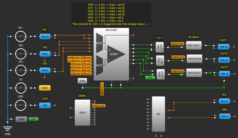
Figure 1. MS-ACMP design block diagram
The main characteristics of the MS-ACMP
The SLG47001/3 has one multi-channel sampling analog comparator (MS-ACMP) that can take periodic samples from up to six input channels and latches the results at the six outputs (Figure 2). The available inputs for the MS-ACMP consist of the following: GPIO0, GPIO1, GPIO2, GPIO3, OA0_OUT, OA1_OUT, RH1A, RH1B, TS_OUT, or VDD. GPIO8 and GPIO9 are also available in STQFN-24 package option. Users can select from one to six channels to be sampled (for example, Channel0, Channel1, and Channel2).
The channels are sampled in fixed order from Channel0 to Channel5. Each channel has an individual voltage reference with programmable low-to-high and high-to-low thresholds. The VREF voltage ranges from 32 mV to 2016 mV with 32 mV steps, and each channel has two separate registers, 6-bit for the low-to-high VREF threshold and another 6-bits for the high-to-low VREF threshold selection. The non-inverting input of the MS-ACMP has a voltage divider (Gain of 1, 1/2, 1/3, and 1/4) that can configure the gain of each channel individually.
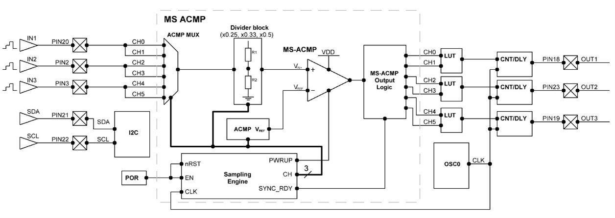
Figure 2. MS-ACMP typical application circuit
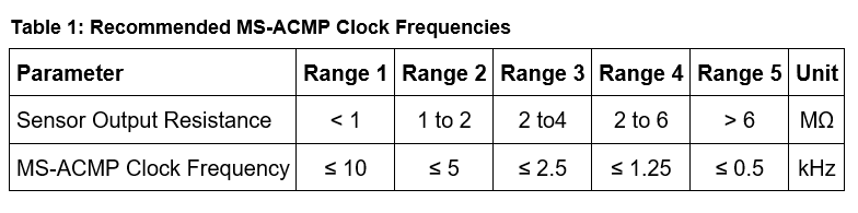
The MS-ACMP uses the internal oscillator (OSC0) or an external clock (max. 10 kHz with 50% duty cycle) to switch between channels, change VREF, and latch the results. The clock from OSC0 can be divided by 2, 4, or 8 within the MS-ACMP. If the ‘Auto Power-on’ setting of OSC0 is selected, a HIGH-level voltage (or a rising edge depending on the setting) on the EN input starts the internal oscillator (OSC0). Table 1 shows the recommended MS-ACMP clock frequencies when interfacing sensors with high output impedance.
The outputs of the MS-ACMP can be configured to be either asynchronous or synchronous.
In asynchronous mode (ACMP_SYNC_MODE = 0), the results appear continuously after each channel is sampled.
In synchronous mode (ACMP_SYNC_MODE = 1), the results at the output appear simultaneously after the last selected channel is sampled.
This design for the MS-ACMP uses sampling mode (ACMP_RNG_MODE = 0) with Level-sensitive Detection (ACMP_DET_MODE = 0). In this mode, the MS-ACMP switches between up to six sampled channels and latches the result every pulse at the CLK input while the EN input is high. When the EN signal goes low, the MS-ACMP finishes the sampling sequence and enters power-down mode.
Design Operation
- MS-ACMP Settings:
- VDD input: Disable (default)
- Temp Sensor input: Disable (default)
- Force bandgap on: Enable (default)
- Output nReset: Connected to POR
- Hysteresis: Hysteresis options for each channel are disabled (0 mV).
- IN+ Gain: For channel CH0, CH1 – x0.33; For channel CH2, CH3 – x0.25; For channel CH4, CH5 – x0.5.
Connections:
- IN+ CH0: Non-inverting analog input source terminal of Channel 0. (GPIO8)
- IN+ CH1: Non-inverting analog input source terminal of Channel 1. (GPIO8)
- IN+ CH2: Non-inverting analog input source terminal of Channel 2. (GPIO1)
- IN+ CH3: Non-inverting analog input source terminal of Channel 3. (GPIO1)
- IN+ CH4: Non-inverting analog input source terminal of Channel 4. (GPIO0)
- IN+ CH5: Non-inverting analog input source terminal of Channel 5. (GPIO0)
- IN- CH0: Inverting analog input source terminal of Channel 0. (1056 mV Vref)
- IN- CH1: Inverting analog input source terminal of Channel 1. (1120 mV Vref)
- IN- CH2: Inverting analog input source terminal of Channel 2. (576 mV Vref)
- IN- CH3: Inverting analog input source terminal of Channel 3. (672 mV Vref)
- IN- CH4: Inverting analog input source terminal of Channel 4. (800 mV Vref)
- IN- CH5: Inverting analog input source terminal of Channel 5. (928 mV Vref)
- CLK: Sampling clock source of MS ACMP. (Default – OSC0)
- Enable: Connect Enable matrix input through a POR
- nReset: Connect nReset matrix input through a POR
- OUT CH0: Connect to IN1 (2-bit LUT0)
- OUT CH1: Connect to IN0 (2-bit LUT0)
- OUT CH2: Connect to IN1 (2-bit LUT1)
- OUT CH3: Connect to IN0 (2-bit LUT1)
- OUT CH4: Connect to IN2 (3-bit LUT0)
- OUT CH5: Connect to IN1 (3-bit LUT0)
MS-ACMP Channel Configuration:
- IN- CH0: Threshold
- IN- CH1: Threshold
- IN- CH2: Threshold
- IN- CH3: Threshold
- IN- CH4: Threshold
- IN- CH5: Threshold
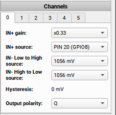
Figure 3. Channel Configuration
Operating Principle
Input Signal Multiplexing:
- The analog multiplexer selects the input signal for comparison with the corresponding threshold.
- The signal on each input is checked using the comparator.
Comparison
The system utilizes two comparators to perform window comparison. The first comparator compares the input signal with the lower threshold value. If VIN_CH0 > VTH0, its digital output “MS ACMP OUT CH0” transitions to a “HIGH” state (logical 1). Similarly, the second comparator compares the input signal with the upper threshold. If VIN_CH1 > VTH1, the MS-ACMP’s digital output also transitions to a “HIGH” state (logical 1). Both digital outputs of the comparator are processed by a 2-bit LUT logic block, which generates the system’s output signal. For example, as a result, the output signal is set to a high state only when the input voltage is within the specified range. For the OUT1 output, this range is 3.2 V to 3.4 V.
Otherwise, the MS ACMP output transitions to a “LOW” state (logical 0).
Signal Generation
Each output generates a signal that can be used for monitoring or control purposes. However, it is recommended to additionally add a CNT/DLY block at the output.
Delay blocks are used in the circuit to generate stable pulses at the output. In this case, the CNT/DLY block performs dual functions:
- Stabilization of output signals. The comparator analyzes input signals and determines when the voltage level exceeds a certain threshold. However, if the input signal is at the switching threshold, the CNT/DLY macrocell helps reduce the risk of false triggering by maintaining the signal state (high/low) for a set period before the next transition.
- Glitch filtering. Without the DLY block, the circuit may respond to short voltage spikes. Adding this block makes it possible to filter out short pulses that do not correspond to actual signal changes.
Synchronization
The SYNC READY signal indicates the completion of the multiplexing process and readiness for a new processing cycle.
Design Software Simulation
Input Signals (IN1, IN2, IN3)
Input voltages vary over time across different ranges.
Digital Outputs (OUT CH0, OUT CH1, OUT CH2, OUT CH3, OUT CH4, OUT CH5)
Outputs switch to a “HIGH” state at points where VIN_CHi > VTHi. For example, OUT_CH0 is activated when VIN_CH0 > 3.26 V, and OUT_CH1 is activated when when VIN_CH1 > 3.4 V.
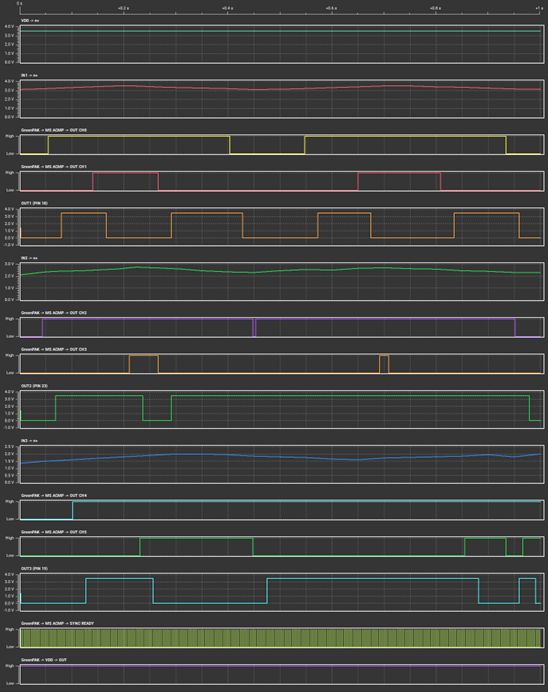
Figure 4. MS-ACMP Input/Output graphs
Conclusion
In conclusion, this six-channel analog comparator system, built around the MS-ACMP of the Renesas SLG47003,offers a precise and flexible solution for monitoring three distinct voltage levels with high reliability. By utilizing internal reference generators and configurable gain settings, the design maintains accuracy even under fluctuating supply conditions. Its versatility makes it well-suited for a range of applications, including battery and power supply monitoring, overvoltage/undervoltage protection systems, and voltage-triggered automation tasks. Whether for safeguarding critical circuits or enabling smart control, this implementation provides a robust foundation for modern analog monitoring solutions.
Images used courtesy of Renesas


