MYIR Launched RENESAS RZ/G2L based SoM for HMI and Edge Gateway Applications
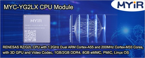
MYIR has launched MYC-YG2LX CPU Module based on RENESAS RZ/G2L SoC which features 1.2GHz dual ARM Cortex-A55 and 200MHz Cortex-M33 cores with high-performance Mali-G31 GPU and built-in video codec engine as well as various peripheral interfaces such as camera input, display output, USB 2.0, and GigE-Ether. In addition to the SoC, the MYC-YG2LX has integrated 1GB/2GB DDR4, 8GB eMMC, 32Kbit EEPROM and PMIC.
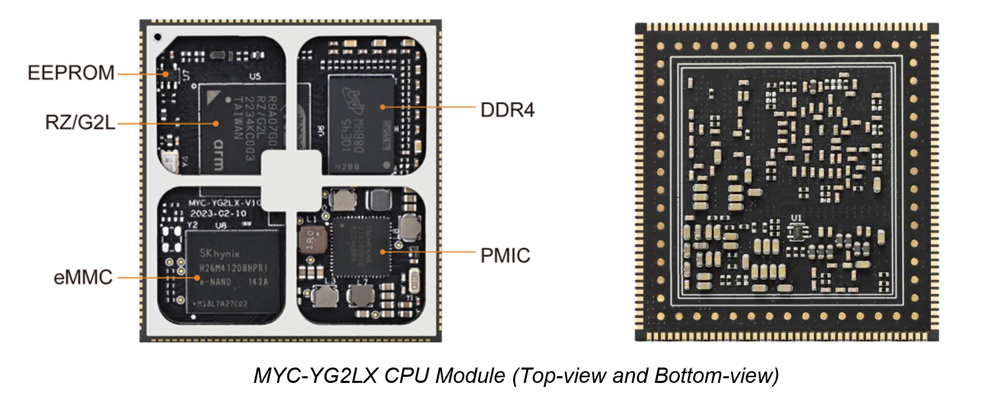
MYIR has launched MYC-YG2LX CPU Module based on RENESAS RZ/G2L SoC which features 1.2GHz dual ARM Cortex-A55 and 200MHz Cortex-M33 cores with high-performance Mali-G31 GPU and built-in video codec engine as well as various peripheral interfaces such as camera input, display output, USB 2.0, and GigE-Ether. In addition to the SoC, the MYC-YG2LX has integrated 1GB/2GB DDR4, 8GB eMMC, 32Kbit EEPROM and PMIC. A variety of peripheral and IO signals are accessible via the 1.0 mm pitch 222-pin Castellated-Hole expansion interface. It provides a cost-effective SoM solution for advanced HMI, IoT Edge Computing Gateway and embedded devices with video capabilities.
The MYC-YG2LX CPU Module has a small form factor, measuring only 45mm by 43mm. It is ready to run Linux OS and provided with image files, kernel and driver source codes, application demos and compilation tools to enable users to start their development rapidly and easily.
Features Of MYC-YG2LX CPU Module
- Dimensions: 45mm x 43mm
- PCB Layers: 10-layer design
- Power supply: 5V/1A
- Working temperature: -40~85 Celsius (industrial grade)
- RENESAS RZ/G2L processor (R9A07G044L23GBG)
- 1G/2G DDR4 (supports optional 4GB)
- 8GB eMMC (supports optional 4GB, 16GB / 32GB)
- 32KB EEPROM
- Power Management IC (RAA215300)
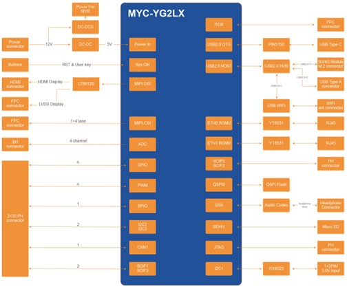
- 0mm pitch 222-pin stamp hole expansion interface
– 2 x RGMII
– 4 x I2C
– 3 x SPI
– 2 x USB 2.0
– 1 x MIPI DSI
– 1 x MIPI CSI
– 1 x Parallel CSI
– 1 x RGB
– 2 x SCI
– 5 x SCIF
– 8 x ADC
– 4 x SSI
– 1 x SRC
– 2 x CAN
– Up to 118 GPIOs
Note: the peripheral signals brought out to the expansion interface are listed in maximum number. Some signals are reused. Please refer to the processor datasheet and CPU Module pin-out description file.
- Linux OS
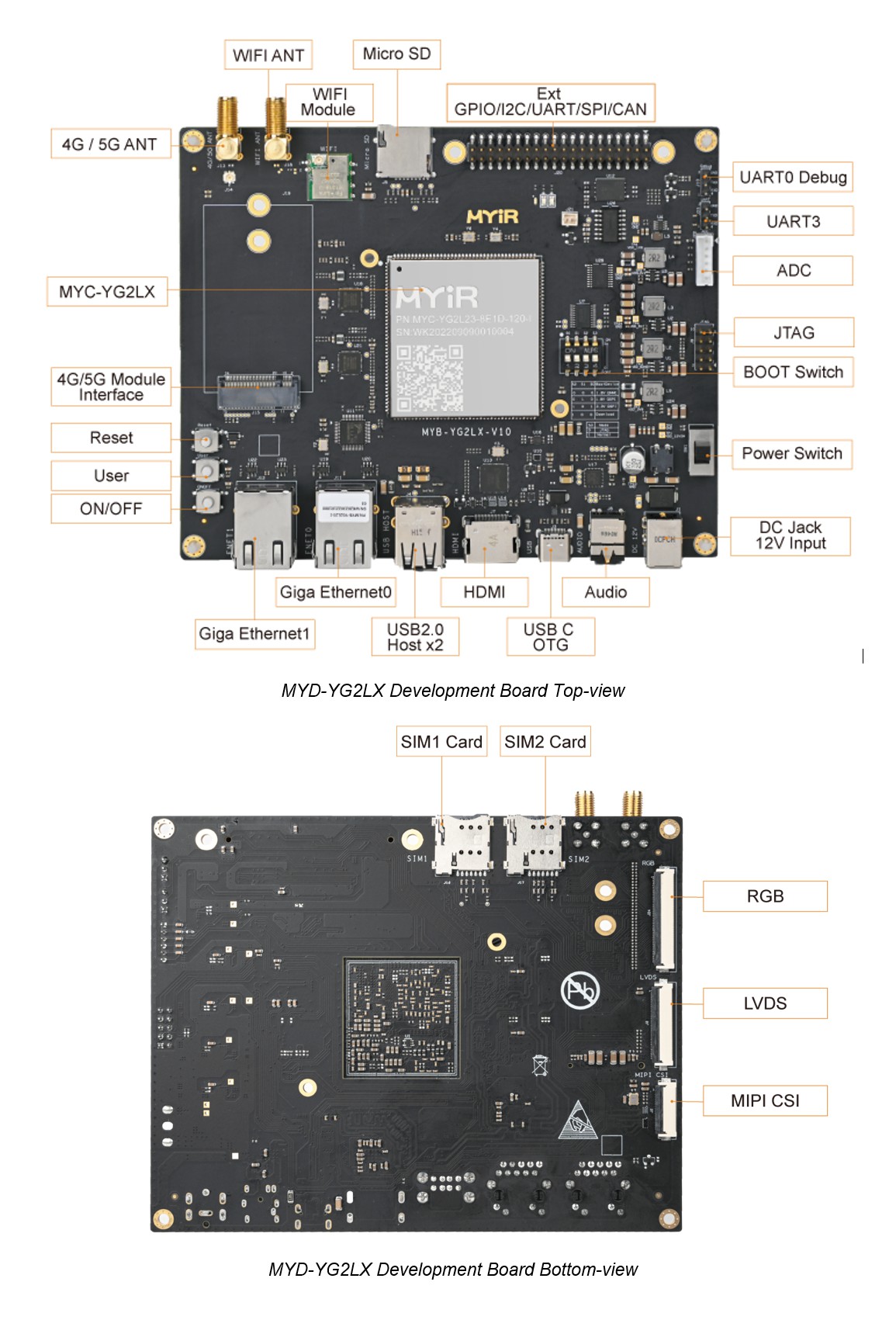
MYIR has designed a versatile development board MYD-YG2LX, using the MYC-YG2LX CPU Module as core controller module. It is a complete evaluation platform and has provided an ideal base board prototype reference design for using the MYC-YG2LX. A plenty of peripherals interfaces are carried out to the base board through the 1.0 mm pitch 222-pin Castellated-Hole expansion interface including Serial ports, two Gigabit Ethernet, two USB 2.0 HOST and one USB 2.0 OTG, one Micro SD card slot, one M.2 Socket for USB based 4G/5G LTE Module with two SIM card holders, one USB2.0 based WiFi module, one GPIO/I2C/UART/SPI/CAN extension header, Audio input/output, MIPI-CSI camera interface as well as HDMI, LVDS and RGB video output interfaces, etc. MYIR also offers camera modules, RPI COM Module (RS232/RS485/CAN) and LCD modules as add-on options to work with the board for further enhancing the functionality of the board.
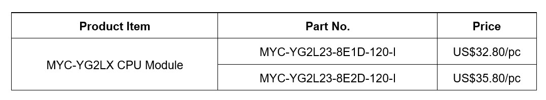
MYIR offers 1GB and 2GB DDR4 version options for the MYC-YG2LX CPU Module. The prices are economic but the module has high performance and reliable quality. Discount is to be offered for volume quantities. MYIR also provides OEM/ODM services to help customers accelerate their time to market and save costs.
More information about the above new products can be found at: https://www.myirtech.com/list.asp?id=719


