
Nisshinbo’s Silicon Motherboard Merges ICs and Passives On-Die
A new double-sided packaging method embeds resistors, capacitors, and inductors alongside active dies, cutting footprint by roughly 80 percent.
Nisshinbo Micro Devices has unveiled Silicon Motherboard (Si-MB®), a three-dimensional packaging approach the company says is the first to place functional circuitry on both faces of a silicon substrate. The technique integrates active dies and passive components into a single unit and, in an early prototype, reduced the overall mounting footprint by about 80 percent compared with a conventional discrete layout.
Closing the Gap Left by Chiplets
Component counts inside industrial, automotive, and communications equipment have been climbing as those products gain functionality, and that growth carries consequences beyond size: bulkier assemblies raise transportation energy use and complicate parts sourcing. Chiplet packaging has offered one path toward denser, smaller assemblies, but the architecture is built around stacking IC dies and struggles to accommodate discrete passives such as chip resistors and capacitors. The high-density chiplets also tend to come at the expense of ruggedness, narrowing the technology’s deployment range.
Silicon Motherboard targets that gap directly. Functional chips sit on the substrate’s top surface, while transistors, resistors, and capacitors are formed within the substrate itself through wafer processing. External passives, including large-value capacitors above 1,000 pF, sub-1 Ω resistors, and inductors, are then mounted on the underside — components that conventional chiplet structures generally cannot house.
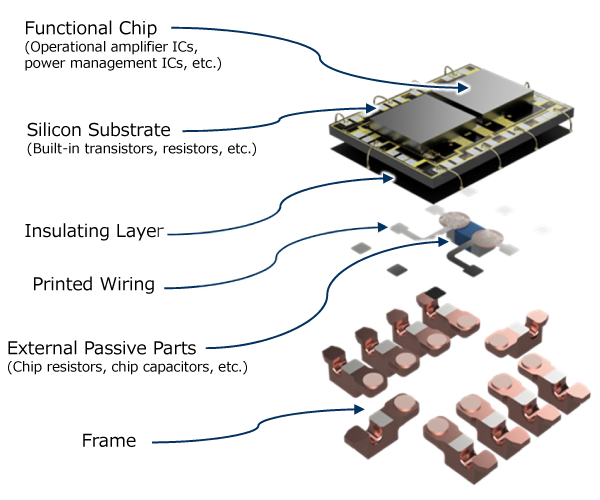
Silicon Motherboard’s six-layer structure separates on-die active circuitry from external passive components mounted on the underside of the substrate. Image used courtesy of Nisshinbo
Built Around an Existing Package Footprint
Rather than introducing a new package outline, Silicon Motherboard reuses shapes already common in mass production. That choice lets engineers use their existing placement equipment without qualifying new hardware, shortening evaluation cycles and trimming implementation costs. It also broadens the range of applications where the technology fits, spanning consumer designs as well as industrial and automotive applications that demand higher reliability.
Nisshinbo built a working prototype around a window-comparator function to demonstrate the approach. Two comparator ICs were mounted as functional chips on the substrate; resistive elements were formed within the substrate through wafer processing; and two chip resistors were placed on the underside wiring. That combination produced a roughly 80 percent footprint reduction compared to a comparable discrete build.
The company points to its background in low-noise, high-precision analog IC design — a portfolio that includes leading shares of the global op-amp, comparator, and LDO markets — as the foundation for the new packaging work. Analog IC performance depends heavily on the passives and layout surrounding the die, and Nisshinbo frames Silicon Motherboard as a way to optimize the active and passive elements as a single system rather than as separately sourced parts.
Looking beyond individual IC sales, Nisshinbo plans to extend this packaging approach into complete system solutions that bundle peripheral components with its analog ICs. For design teams working on space-constrained boards in industrial, automotive, or communications gear, that combination could simplify sourcing while opening up circuit configurations that discrete layouts and chiplet stacks couldn’t easily support.


