ROHM’s AW2K21 MOSFET is a New Benchmark for Low ON-Resistance
The new N-channel MOSFET achieves an industry-leading low ON-resistance per unit area, reducing footprint by over 80% and improving efficiency for fast charging applications.
In the ever-growing market of portable electronics, the demand for smaller, more powerful, and faster-charging devices places significant pressure on power component engineers. ROHM Semiconductor’s latest offering, the AW2K21 N-channel MOSFET, is designed to directly address these challenges, leveraging a WLCSP2020 package to deliver a combination of low ON-resistance and a minimal footprint.
High-Density Current Capacity in a Space-Saving Design
The AW2K21 MOSFET is a 30V, N-channel device with a common source configuration, housed in a compact 2.0mm x 2.0mm x 0.55mm WLCSP2020 package. Its most notable characteristic is its low typical ON-resistance of 2.0 mΩ (at VGS=5.0V, ID=20A), a metric that the company claims is an industry-leading value per unit area for its class. This performance is a direct result of advancements in chip design and packaging technology, which allow for a higher density of current-carrying capacity within a smaller form factor.

The AW2K21 is designed to provide longer battery life and faster charging time in a small footprint. Image used courtesy of ROHM.
From a design perspective, the low ON-resistance is critical for minimizing power loss (P = I²R) and thermal dissipation in high-current applications. The AW2K21’s specifications indicate a significant leap in this regard. Compared to typical dual-MOSFET solutions that might be used to achieve similar performance levels, a single AW2K21 can replace two 3.3mm x 3.3mm MOSFETs. This consolidation not only reduces the total circuit board footprint by approximately 81% but also lowers the overall ON-resistance by about 33%. This efficiency gain is particularly important for battery-powered devices where every milliwatt saved extends battery life and reduces charging times.
The AW2K21’s performance also stacks up favorably against alternative technologies, such as Gallium Nitride (GaN) high-electron-mobility transistors (HEMTs). While GaN devices are often heralded for their high-frequency and low-loss characteristics, the AW2K21 can achieve up to a 50% reduction in ON-resistance compared to similarly sized GaN HEMTs, according to the press release. This positions the AW2K21 as a compelling alternative for applications where ultra-low ON-resistance in a compact form factor is a higher priority than extreme high-frequency switching.
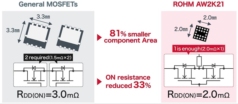
Comparison of a general MOSFET solution to the ROHM AW2K21. Image used courtesy of ROHM.
The target applications for the AW2K21 are primarily in high-power fast charging and unidirectional load switching. These include a wide array of consumer electronics such as smartphones, tablets, laptops, and wearables, as well as more specialized devices like drones and VR headsets. The ability to manage high-drain currents of up to ±20A within such a small package makes it a robust choice for these demanding power management scenarios.
Summary
For electrical engineers, this new MOSFET represents more than just a component with improved specs; it’s a tool for designing more compact, cooler-running, and more efficient power stages. The reduction in footprint and ON-resistance enables designers to either shrink their power management circuits or utilize the saved board space for other components, all while improving the overall thermal performance and power efficiency of the end product. As the trend towards smaller and more powerful devices continues, components like the AW2K21 will be instrumental in meeting the increasingly stringent design requirements of the future.


