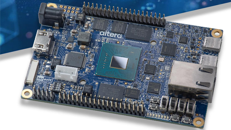
Terasic DE25-Nano FPGA Development Board with Agilex 5 SoC and ARM HPS
The DE25-Nano combines Intel Agilex 5 FPGA, dual ARM Cortex cores, and versatile interfaces, offering a powerful platform for prototyping and embedded system design.
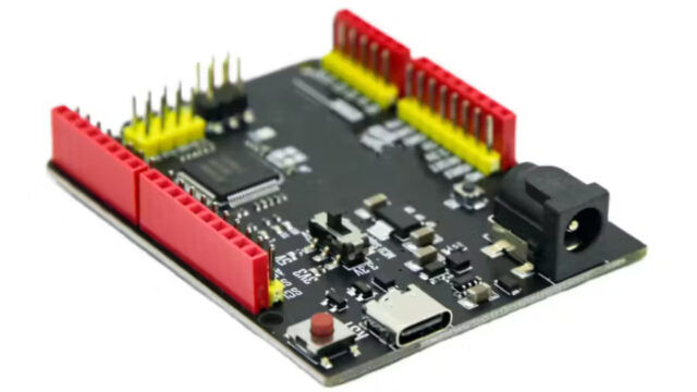
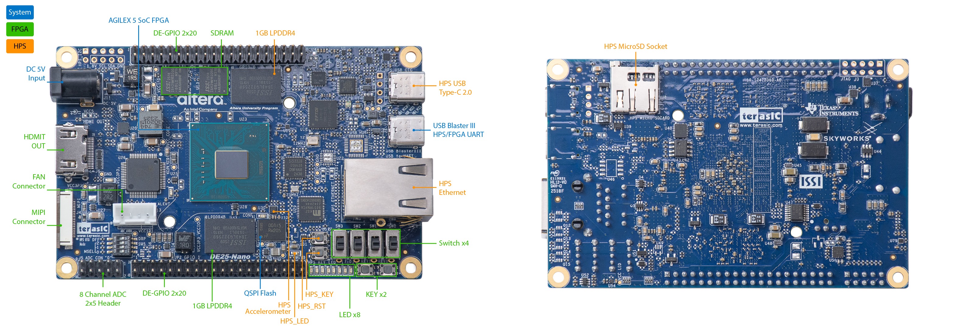
DE25 NANO FPGA development board
In embedded systems and accelerator hardware, an FPGA development board serves as a key tool for prototyping, education, and production. Engineers rely on these boards to test hardware concepts, interface with peripherals, and validate real-time logic before moving to custom silicon or final system designs.
A strong addition to this category is the Terasic DE25-Nano, built around Intel/Altera’s Agilex 5 SoC. It combines programmable logic with a dual-cluster ARM HPS and a versatile I/O set, making it suitable for applications such as edge AI, vision processing, and robotics.
Previously, we covered FPGA development boards such as the Alchitry Au V2, Tang Mega 138K Pro Dock, ICE-V Wireless Mini, and the STEPFPGA series and more. You can check those articles for more details.
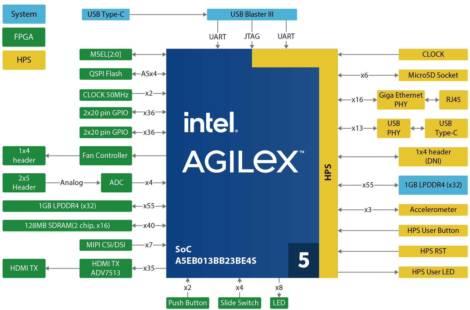
Intel’s Agilex 5 FPGA Block Diagram
DE25 NANO FPGA development board Specifications:
- FPGA Device:
- Intel Agilex 5 SoC FPGA (A5EB013BB23BE4SR1)
- ~138K programmable logic elements (LEs)
- 8.42 Mbit embedded memory
- 376 x 18 x 19 multipliers for DSP workloads
- Integrated ARM Cortex-A76 (x2) + Cortex-A55 (x2) HPS subsystem
- Memory:
- 128 MB SDRAM connected to FPGA fabric
- 1 GB LPDDR4 dedicated to FPGA
- 1 GB LPDDR4 shared between FPGA and HPS
- MicroSD card socket for storage and OS image
- Configuration and Debug:
- Onboard USB-Blaster III programmer via USB Type-C
- Supports ASx4 configure mode with 128 Mbit QSPI Flash
- Communication Interfaces:
- Gigabit Ethernet port (10/100/1000 Mbps)
- USB 2.0 host port via Type-C connector
- UART-to-USB bridge over Type-C
- Sensors:
- Accelerometer (G-sensor) linked to HPS
- Temperature sensor tied to FPGA fabric
- Expansion Connectors:
- Two 40-pin DE-GPIO expansion headers (FPGA I/O, power rails)
- One 10-pin ADC input header
- Display and Camera:
- HDMI 2.0 output port (up to 1080p resolution)
- One MIPI D-PHY v2.5 connector with 2 data lanes
- Analog-to-Digital Converter (ADC):
- 8-channel, 12-bit resolution
- SPI interface
- 1 MSPS throughput rate
- Analog input range: 0 V to 3.4 V
- Misc:
- 4x user switches (FPGA-controlled)
- 5x user pushbuttons (4 FPGA + 1 HPS)
- 9x user LEDs (8 FPGA + 1 HPS)
- HPS cold reset button
- Thermal and Cooling:
- Active heatsink with fan controller
- Real-time temperature monitoring for thermal stability
- Power: 5V DC input power supply
- Dimensions: 106.92 x 68.58 mm
DE25 NANO FPGA development board Specifications
On the software side, the DE25-Nano works with Intel Quartus Pro for FPGA synthesis, place-and-route, and bitstream generation. Terasic provides a board support package (BSP) that includes reference designs for communication between the ARM HPS and FPGA fabric. Developers can boot Linux on the HPS, run drivers or applications, and offload compute-intensive logic to the FPGA. The shared memory architecture enables efficient interaction between hardware and software, delivering high throughput and low-latency performance.

Connection to 2×20 GPIO Daughter Card. Images used courtesy of Electrotrio.
The DE25-Nano FPGA development board is available through Terasic’s official website. The standard edition costs $248, while the academic version is offered at a reduced price of $207. An optional USB WiFi dongle can be added for $8. Full details and ordering options are listed on the Terasic DE25-Nano product page.
Images used courtesy of Terasic and Electrotrio.