


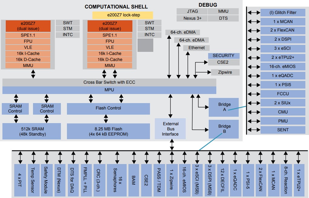
NXP Semiconductors MPC5777C Power Architecture® Microcontroller is a high-performance, multicore MCU optimized for industrial and automotive control applications that require advanced performance, timing systems, security, and functional safety capabilities. The MPC5777C features two independent Power Architecture z7 cores with up to 300MHz operation, along with a single z7 core in Lockstep with one of the main cores. Integrated eTPU timers and Sigma-DeltaADC converters allow for advanced filtering using on-chip knock hardware. On-chip security encryption protection, using CSE and TDM for tamper proofing, help support ASIL-D and SIL-1 functional safety (ISO26262/ IEC61508) requirements.
The MPC5777C Power Architecture® Microcontroller is offered in a Pb-free 416-ball and 516-ball Molded Array Process Ball Grid Array (MAPBGA) package.
Features
- Three dual-issue, 32-bit CPU core complexes (e200z7), two of which run in lockstep
- Power Architecture embedded specification compliance
- Instruction set enhancement allowing variable length encoding (VLE), optional encoding of mixed 16-bit and 32-bit instructions, for code size footprint reduction
- On the two computational cores: Signal processing extension (SPE1.1) instruction support for digital signal processing (DSP)
- Single-precision floating point operations
- On the two computational cores: 16 KB I-Cache and 16 KB D-Cache
- Hardware cache coherency between cores
- 16 hardware semaphores
- 3-channel CRC module
- 8MB on-chip flash memory
- Supports read during program and erase operations, and multiple blocks allowing EEPROM emulation
- 512KB on-chip general-purpose SRAM including 64 KB standby RAM
- Two multichannel direct memory access controllers (eDMA)
- 64 channels per eDMA
- Dual core Interrupt Controller (INTC)
- Dual phase-locked loops (PLLs) with stable clock domain for peripherals and frequency modulation (FM) domain for computational shell
- Crossbar Switch architecture for concurrent access to peripherals, flash memory, or RAM from multiple bus masters with End-To-End ECC
- External Bus Interface (EBI) for calibration and application use
- System Integration Unit (SIU)
- Error Injection Module (EIM) and Error Reporting Module (ERM)
- Four protected port output (PPO) pins
- Boot Assist Module (BAM) supports serial bootload via CAN or SCI
- Three second-generation Enhanced Time Processor Units (eTPUs)
- 32 channels per eTPU
- Total of 36KB code RAM
- Total of 9KB parameter RAM
- Enhanced Modular Input/Output System (eMIOS) supporting 32 unified channels
- Two Enhanced Queued Analog-to-Digital Converter (eQADC) modules with:
- Two separate analog converters per eQADC module
- Support for a total of 70 analog input pins, expandable to 182 inputs with off-chip multiplexers
- Interface to twelve hardware Decimation Filters
- Enhanced “Tap” command to route any conversion to two separate Decimation Filters
- Four independent 16-bit Sigma-Delta ADCs (SDADCs)
- 10-channel Reaction Module
- Ethernet (FEC)
- Two PSI5 modules
- Two SENT Receiver (SRX) modules supporting 12 channels
- Zipwire: SIPI and LFAST modules
- Five Deserial Serial Peripheral Interface (DSPI) modules
- Five Enhanced Serial Communication Interface (eSCI) modules
- Four Controller Area Network (FlexCAN) modules
- Two M_CAN modules that support FD
- Fault Collection and Control Unit (FCCU)
- Clock Monitor Units (CMUs)
- Tamper Detection Module (TDM)
- Cryptographic Services Engine (CSE)
- Complies with Secure Hardware Extension (SHE) Functional Specification Version 1.1 security functions
- Includes software selectable enhancement to key usage flag for MAC verification and increase in number of memory slots for security keys
- PASS module to support security features
- Nexus development interface (NDI) per IEEE-ISTO 5001-2003 standard, with some support for 2010 standard
- Device and board test support per Joint Test Action Group (JTAG) IEEE 1149.1 and 1149.7
- On-chip voltage regulator controller (VRC) that derives the core logic supply voltage from the high-voltage supply
- On-chip voltage regulator for flash memory
- Self Test capability
- Package options: MAPBGA-416, MAPBGA-516
Block Diagram
more information: www.nxp.com
RELATED POSTS
 6 February, 2020 SEGGER Releases Floating-Point Library to Support RISC-V
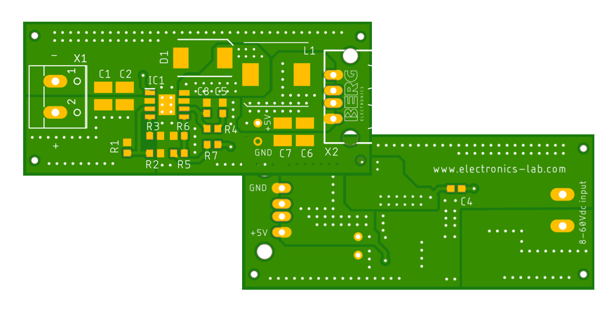 14 March, 2019 JLCPCB.com – Eagle Gerber Export and Quick PCB Review
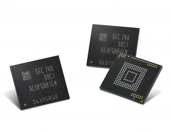 15 December, 2017 512Gbyte embedded universal flash memory in production
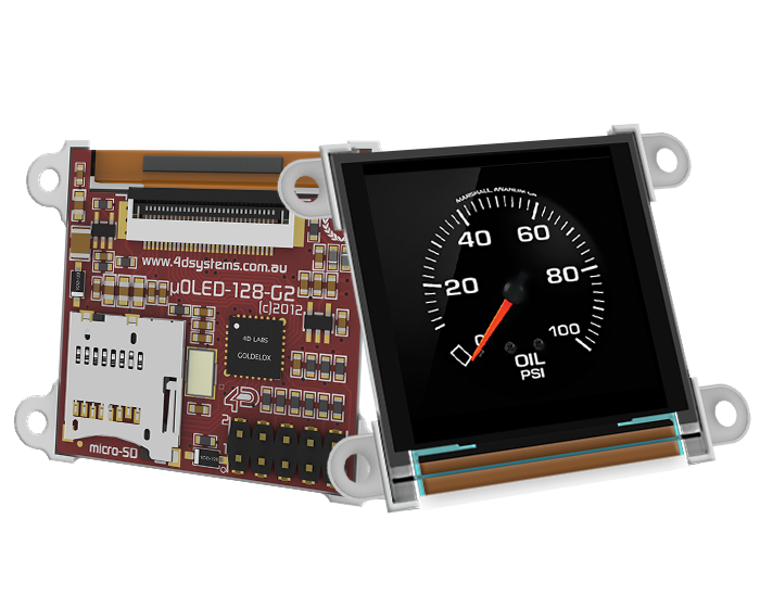 11 December, 2020 UOLED-128-G2 – 1.5″ Smart micro OLED Display
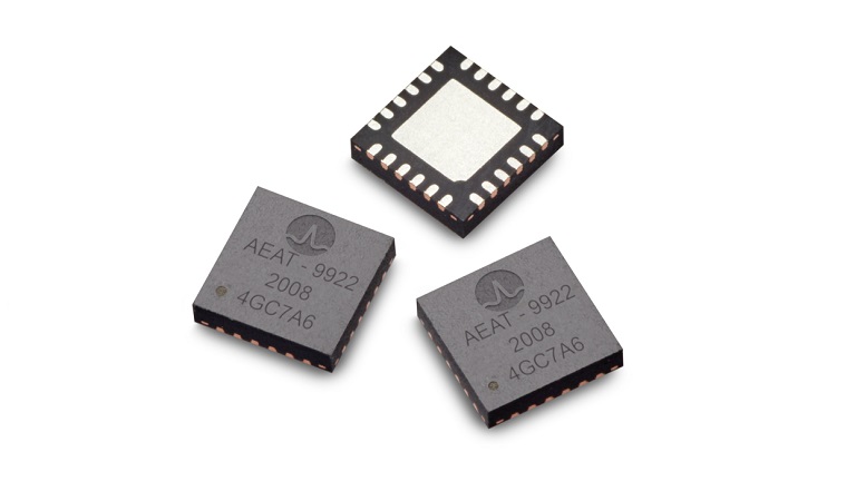 12 April, 2021 Broadcom AEAT-9922 10-Bit to 18-Bit programmable magnetic encoder
 3 July, 2019 FireAnt – A low-cost, thumb-sized, breadboard-friendly FPGA dev board