AOS Launches Low- and Medium-Voltage MOSFETs With Double-Sided Cooling
The new AONC40202 25 V and AONC68816 80 V MOSFETs are available in a DFN 3.3×3.3 source-down packaging with double-sided cooling and a center-gate layout for AI servers and data centers.
Alpha and Omega Semiconductor (AOS) has introduced two new N-channel MOSFETs — the AONC40202 at 25 V and the AONC68816 at 80 V — both housed in a DFN 3.3×3.3 source-down package with double-sided cooling. The devices are aimed at DC-DC Intermediate Bus Converter stages in AI servers and data centers, where thermal headroom is increasingly hard to come by.
A Package Built Around Heat Removal
The headline feature of the two new MOSFETs is their double-sided thermal interface. A large optimized top clip exposes the drain contact on the top surface, while the source-down orientation puts a large source pad in contact with the PCB below. Heat can therefore leave the device from both faces simultaneously, rather than relying on a single conduction path.

The new AONC40202 25 V MOSFET and AONC68816 80 V MOSFETs are designed for AI servers and data centers. Image used courtesy of Alpha and Omega Semiconductor
Both devices share a top-side thermal resistance (Rthc-top) of 0.9°C/W and a bottom-side thermal resistance (Rthc-bottom) of 1.1°C/W. According to AOS, this arrangement outperforms traditional single-sided DFN 3.3×3.3 packages in terms of thermal stress and heat generation. The maximum junction temperature for both parts is 175°C, and each is 100% UIS- and Rg-tested in production.
The center-gate pin layout is a practical benefit worth noting. Because the gate pin sits at the center of the package rather than at a corner, PCB routing to the gate driver is shorter and more symmetrical — a useful detail when switching at high frequency, where parasitic inductance in the gate loop matters.
AONC40202 and AONC68816 MOSFETs
The AONC40202 is the lower-voltage part of the pair, using AOS’s AlphaSGT 25 V silicon technology. It achieves an RDS(ON) of 0.63 mΩ typical at VGS = 10 V and handles a continuous drain current of 405 A at 25°C, rising to a pulsed peak of 644 A. The total gate charge Qg at 10 V is 83 nC typical, and the reverse recovery charge Qrr is 25 nC — reasonable figures for a device in this current class. The datasheet lists synchronous rectification and low-side DC-DC switching as primary applications.
The AONC68816 steps up to 80 V, using AOS’s trench-based AlphaSGT technology at that voltage tier. RDS(ON) is 4.7 mΩ typical at VGS = 10 V, with a continuous drain current of 119 A at 25°C and a pulsed rating of 476 A. Gate charge is considerably lighter than the 25 V part — Qg at 10 V is 42 nC typical — which suits higher-frequency switching topologies. The Qrr of 26 nC is on par with the AONC40202 despite the higher voltage class.
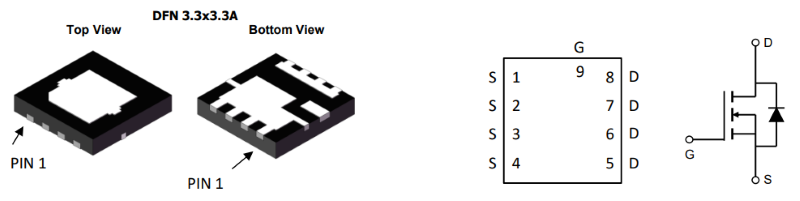
The AONC40202 and AONC68816 MOSFETs are housed in DFN 3.3×3.3 double-sided cooling source-down packaging. Image used courtesy of Alpha and Omega Semiconductor
Both devices sit in the same DFN 3.3×3.3A package and share identical thermal resistance values, simplifying thermal modeling when the two parts are used together in an IBC stage.
Availability
The AONC40202 and AONC68816 are available now in production quantities. Lead time is quoted at 14–16 weeks, with unit pricing of $1.85 and $1.95, respectively, at 1,000-piece quantities. Datasheets for both parts are available on the AOS website.