Logic NAND Gate
Logic NAND Gate The NAND gate is a logic AND gate with an inverted output. It is a reverse or complement of a AND gate discussed previously.
Logic NAND Gate
The NAND gate is a logic AND gate with an inverted output. It is a reverse or complement of a AND gate discussed previously. The logic AND gate output logic “HIGH” when all of its inputs are at logic level “HIGH”. Contrary to this, the logic NAND gate outputs logic “LOW” when all of its inputs are at logic level “HIGH” and it will output a logic “HIGH” when any of its inputs goes to the “LOW” state.
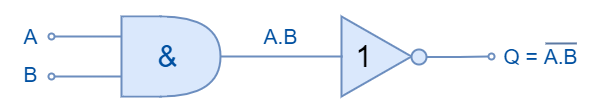
The logic NAND gate can be expressed through logic or Boolean expression of Logical Addition with its inputs inverted. The logic NAND gate Boolean expression is denoted by a dot (.) placed between inputs and an overline. The dot (.) represents a logical multiplication whereas an overline represents a complement (NOT) of inputs. The Boolean expression for a NAND is:
![]()
The logic NAND gate is also referred to as Sheffer Stroke Function and is expressed by a vertical bar or arrow between the inputs.
Resistor-Transistor NAND Gate
In the following figure, a basic two-input NAND gate constructed using Resistor-Transistor Logic (RTL) is shown.
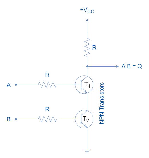
When both inputs “A” and “B” are “HIGH” then both transistors are in saturated “ON” states and a state “LOW” appears at the output (Q). Turning any of the inputs to logic “LOW” will drive the relative transistor to the “OFF” state and pulls the output (Q) high to VCC.
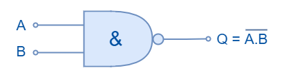
Logic NAND Gate Symbol & Truth Tables
The representation of a NAND logic by a symbol is shown in the following figure. An inversion bubble at the output denotes the inversion of the multiplication.
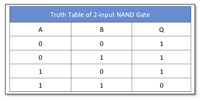
The truth table of a two-input NAND logic gate is shown below:
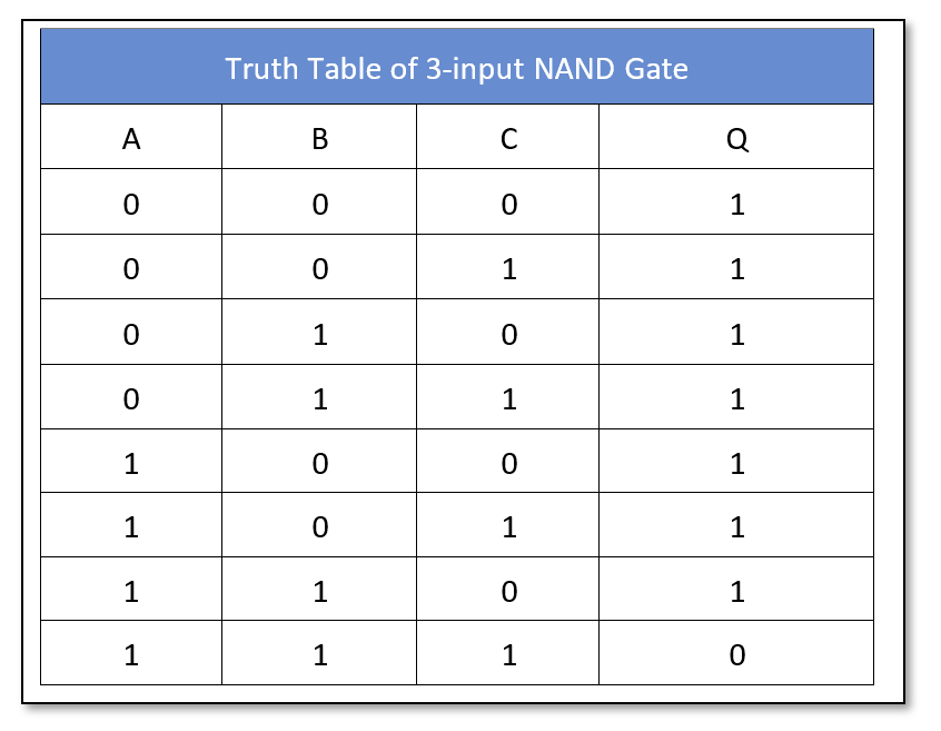
Similarly, the truth table of a three-input NAND logic gate is as follow:
The Boolean expression can be extended to include multiple inputs to obtain a logic NAND operation. The commercially available NAND logic circuits have up to four inputs but the number of inputs can be further extended by cascading the NAND logic circuits. In the following figure, five two-inputs NAND gates are cascaded together to obtain a four-input NAND function.
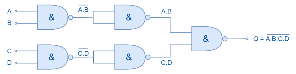
The Boolean expression for this cascaded circuit can be written as:

Odd Number of Inputs
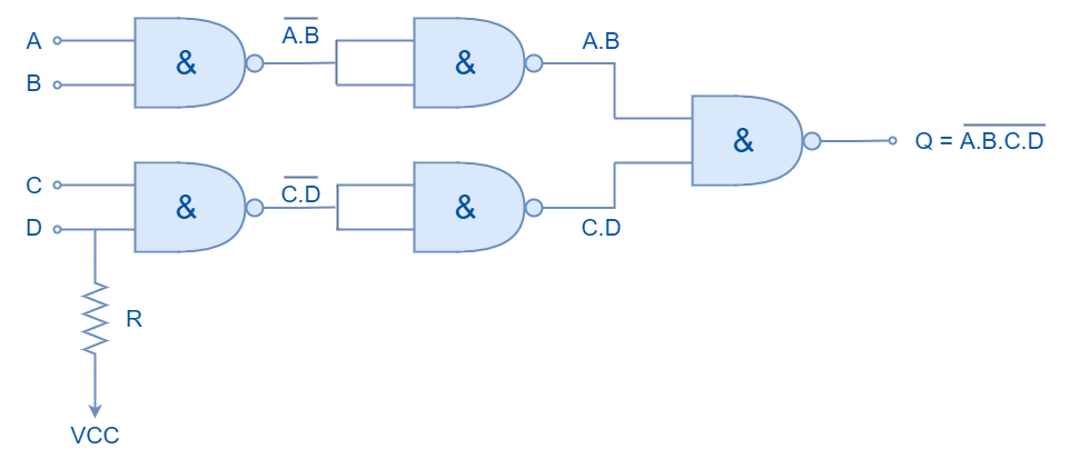
The NAND logic circuit having an odd number of inputs can be constructed by driving the unused input to logic “HIGH”. This will ensure that another input(s) of the NAND logic gate is truly reflected in the output. It is explained in the following diagram where unused input is pulled high using a pull-up resistor.
Universal Gate
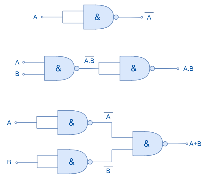
The logic NAND gate is described as a universal gate because it can be used to form the other logics i.e. AND, OR, NOT, Exclusive OR, Exclusive NOR, and NOR, etc. It is the most common and widely used logic gate because of its Universal Gating capability. The examples of forming the AND, OR, and NOT logic by using NAND gates are shown in the following figure.
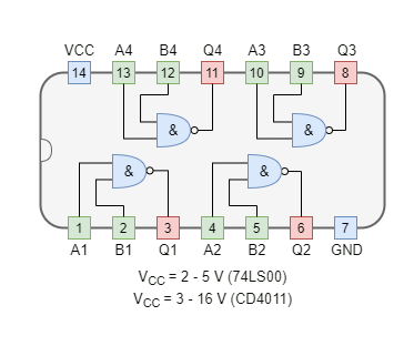
Commercially Available NAND Gates
The NAND logic gates are available in both TTL and CMOS logic families. The most commonly used NAND logic packages are:
CMOS based NAND Gate IC Package
- CD4011 Quad 2-input
- CD4023 Triple 3-input
- CD4012 Dual 4-inputs
TTL based NAND Gate IC Package
- 74LS00 Quad 2-input
- 74LS10 Triple 3-input
- 74LS20 Dual 4-input
- 74LS30 Single 8-input
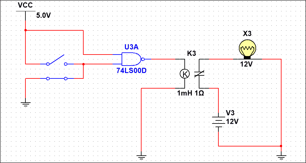
Example of NAND Logic
In the following figure, a NAND gate is used to drive a 12V relay to switch on the lamp using NI Multisim. The NAND gate (74LS00) turns off the relay when all of the inputs are connected to VCC. The relay thus turns off the lamp through an external circuit of 12V. When one of the inputs is connected to Ground, NAND logic goes “ON” turning the relay and lamp to “ON” state.
Conclusion
- The output of the NAND logic is “LOW” when all of the inputs are in logic “HIGH” states.
- Any of the inputs in the logic “LOW” state will drive NAND logic to the “ON” state.
- The NAND gate is sometimes referred to as Sheffer Stroke Function and is denoted by a bar between the inputs.
- The NAND logic gates can be constructed using Resistor-Transistor Logic (RTL) but are seldom used because of the propagation delay and power consumption.
- The NAND gate is termed a Universal Gate because of its capability to form any other logic using only NAND gates.
- The NAND logic gates commercially available have up to eight NAND logic inputs. However, inputs can be extended by using cascaded NAND logic gates.
- The NAND logic circuit having an odd number of inputs can be constructed by using a pull-up resistor on the unused pin.
- An external circuit can be controlled by NAND logic with the use of a magnetic relay.


