Dual Channel SiC MOSFET Gate Driver Reference Design
This reference design is an automotive qualified isolated gate driver solution for driving Silicon Carbide (SiC) MOSFETs in half bridge configuration. The design includes two push pull bias supplies for the dual channel isolated gate driver respectively and each supply provides +15V and -4V output voltage and 1W output power.
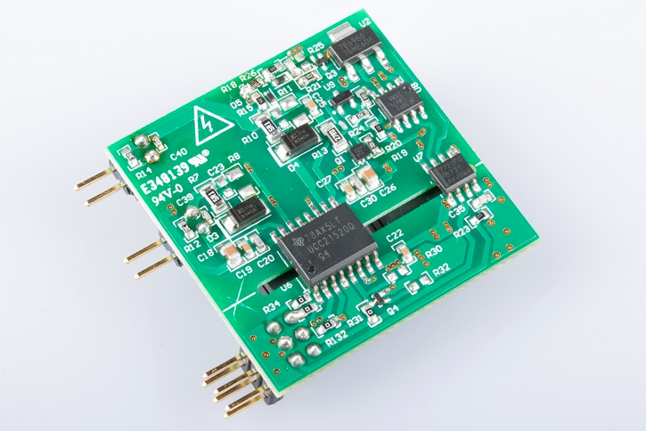
This reference design is an automotive qualified isolated gate driver solution for driving Silicon Carbide (SiC) MOSFETs in half bridge configuration. The design includes two push pull bias supplies for the dual channel isolated gate driver respectively and each supply provides +15V and -4V output voltage and 1W output power. The gate driver is capable of delivering 4A source and 6A sink peak current. It implements reinforced isolation and can withstand 8kV Peak and 5.7kV RMS isolation voltage and >100V/ns common mode transient immunity (CMTI). The reference design contains the two-level turn-off circuit which protects the MOSFET from voltage overshoot during the short circuit scenario. The DESAT detection threshold and the delay time for second stage turn-off are configurable. The ISO7721-Q1 digital isolator is implemented for interfacing the signals of fault and reset. All designed on a two layer PCB board with a compact form factor of 40mm × 40mm.
[source: http://www.ti.com]

