HBM4 Is Here: Samsung Begins Mass Production of Commercial Units
The high-bandwidth memory 4 (HBM4) delivers consistent 11.7 Gbps transfer speeds on its 1c DRAM process node with a 4 nm logic base die.
Samsung Electronics has commenced mass production of high-bandwidth memory 4 (HBM4) and begun shipping commercial units to customers, marking what the company says is a first in the industry. The new memory is built on Samsung’s sixth-generation 10 nm-class DRAM process, referred to internally as “1c,” and incorporates a 4 nm logic-process base die, a departure from the established practice of repurposing proven designs for HBM base-die implementations.
According to Samsung, the transition to newer process nodes was achieved without requiring additional redesigns, and the company reports stable yields from the outset of mass production.
According to Samsung, the HBM4 consistently delivers a processing speed of 11.7 Gbps. Image used courtesy of Samsung Electronics
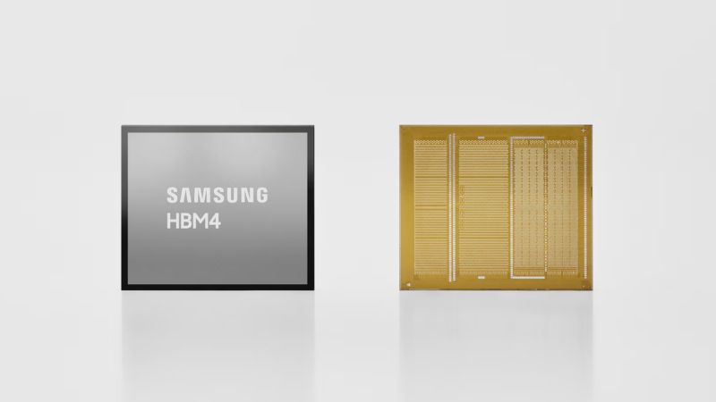
High Bandwidth Memory 4 (HBM4)
Samsung’s HBM4 delivers a consistent transfer speed of 11.7 Gbps per pin, exceeding the JEDEC industry standard of 8 Gbps by roughly 46% and representing a 1.22x increase over the 9.6 Gbps maximum pin speed of HBM3E. The specification can be pushed to 13 Gbps under optimal conditions. Total memory bandwidth per single stack reaches up to 3.3 TB/s, a 2.7x improvement over HBM3E.
The I/O pin count doubles from 1,024 in HBM3E to 2,048 in HBM4, which raises the challenge of managing power and thermal dissipation at scale. Samsung says it has addressed this through low-voltage TSV technology and PDN optimization, claiming a 40% improvement in power efficiency relative to HBM3E. Thermal resistance is reported to improve by 10%, while heat dissipation improves by 30%. HBM4 is available in 24 GB and 36 GB configurations via 12-layer die stacking, with a 16-layer option planned to extend capacity up to 48 GB.

Samsung is currently offering HBM4 in 24 GB to 36 GB capacities via 12-layer stacking. Image used courtesy of Samsung Electronics
Manufacturing and Roadmap
Samsung’s approach integrates “design technology co-optimization” between its Foundry and Memory divisions, with the company citing in-house advanced packaging expertise as a factor in managing production lead times. The company expects its HBM sales to more than triple in 2026 compared to 2025, and production capacity is being expanded accordingly. Sampling for HBM4E is targeted for the second half of 2026, while custom HBM samples are expected to reach customers in 2027.
Samsung also notes plans to expand technical partnerships with GPU manufacturers and hyperscalers focused on next-generation ASIC development.
Where HBM4 Fits
The combination of 3.3 TB/s bandwidth, a 2,048-pin interface, and improved thermal management makes HBM4 a practical option for AI accelerators, HPC systems, and large-scale inference hardware where memory bandwidth is a primary bottleneck. The move to a 4 nm logic base die opens additional flexibility for integrating logic functions closer to the memory stack, which is relevant for architects working on near-memory compute designs. With HBM4E sampling on the horizon and custom configurations to follow, the HBM4 generation is likely to underpin a broad range of next-generation GPU and ASIC platforms through the latter half of this decade.


