

Class A amplifiers
- Boris Poupet
- bpoupet@hotmail.fr
- 10 min
- 11.788 Views
- 0 Comments
- 0 Likes

Introduction
In the introduction tutorial Amplifier Classes, we have presented the different classes of amplification that can be found. In this article, we will focus more in detail about the Class A amplifiers.
Before going into the core of the topic by presenting different Class A configurations, it is important to have in mind the selection criteria of an amplifier class :
- The ratio η=Pout/Pabs that highlights the efficiency of the amplifier.
- The voltage and current gain.
- The distortion which shows how faithfully the output signal is reproduced.
- The maximal working frequency.
It is also important to keep in mind that the class of an amplifier is fully determined from the biasing parameters : the power supply Vsupply, and the resistances of the voltage divider network.
Class A overview
The aim of this section is to get a reminder of the general characteristics of a Class A amplifier before talking about new configurations.
In the case of a Class A amplification, the biasing is chosen such as the operating point is located in the middle of the load line : VC0=Vsupply/2 and IC0=VC0/RC with RC being the resistance of the collector branch.
As seen during the Amplifier Classes tutorial, class A amplifiers have a 360° conduction angle, meaning that 100 % of the input signal is used for the amplification process. Their efficiency is very low with a theoretical maximum of 50 %. We will see in the next section, however, that this last affirmation is valid only for a certain architecture.
Class A configurations are generally low power amplifiers. Moreover, the output load is fixed, that means that they are optimally designed to be connected to a specific load value : either to another amplifier or to a specific loud speaker.
Due to these features, Class A amplifiers are mostly found in the most common type of BJT configuration : the Common Emitter Configuration (CEA). In the next sections, we present two different configurations of Class A amplifiers based on a CEA structure. Everything that we will mention applies to other configurations such as the Common Collector Configuration or the MOSFET.
Basic Common Emitter Configuration in Class A
In this section, we present the basic configuration of a Class A amplifier using the CEA as an example. The output stage of the CEA is shown in Figure 1 below :
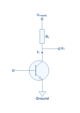
This is the most basic configuration for a Class A power amplifier, note that the load resistance RL is directly wired to the collector branch. In the following, we will refer to this configuration as basic CEAA for Common Emitter Amplifier Class A.
In Figure 2 is presented how the output signal can be decomposed into two components : the biasing DC signal and the AC amplified signal :
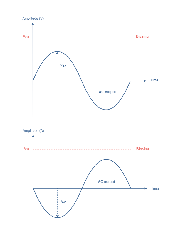
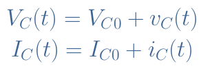
The very visual decomposition of the output signal shown in Figure 2 into one DC component (VC0,IC0) and one AC component (vC(t),iC(t)) allows us to write for the total output signals VC(t) and IC(t) :
For a pure resistive load such as in Figure 1, vC(t)=VAC×sin(ωt) and iC(t)=-IAC×sin(ωt). The symbol ω represents the angular frequency : ω=2πf.
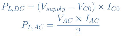
The instant power absorbed by the load PL(t) comes from the contribution of the biasing signal and the alternative signal : PL(t)=(Vsupply-VC(t))×IC(t). It can be shown through an integral calculus over one period of the signal that the average absorbed power PL can be decomposed into one power due to the biasing PL,DC and one useful power due to the signal variations across the load PL,AC :
The total power Ptot supplied to the amplifier comes from the DC power supply : Ptot=Vsupply×IC0. The efficiency of the configuration of Figure 1 is therefore the ratio of the useful power over the total supplied power : η=PL,AC/Ptot.
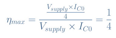
From the expression of PL,AC given in Equation 2, the efficiency is maximum when VAC and IAC are maximized, that is to say for VAC,max=Vsupply/2=VC0 (see why in Figure 3) and IAC,max=IC0.
The maximum efficiency is thus :
All of the information detailed above can be synthesized in the following Figure 3 :
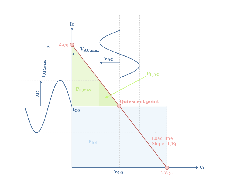
The light blue area represents the total power Ptot supplied to the system. It is very visual here to see that the useful power absorbed to realize the amplification process PL,AC (in light green) represents only a small fraction of Ptot. To overcome to this very low efficiency, one of the solution is coupling the collector branch with a transformer as we will see in the next section.
Transformer-coupled configuration
We present here another configuration of the CEAA that involves the use of a transformer. The following configuration will be referred to as transformer-coupled CEAA. The output stage of this architecture is presented in Figure 4 below :
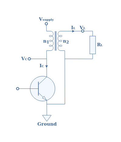
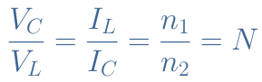
First of all, let’s give a short talk about what a transformer consists of. It is a passive component that transfers energy between two decoupled circuits. It works with generally two inductances wired around a core, the number of turns of the first inductance is n1 and n2 for the secondary circuit. The input (here VC,IC) and output signals (here VL,IL) of a transformer satisfies :
Thanks to the transformer, the load is decoupled from the collector branch, therefore the operating point of the amplifier changes. Indeed, no resistance is interposed between the power supply and the collector branch. Moreover, since the inductance do not block DC voltages, we can consider the DC resistance of the transformer to be equal to zero.
In a basic CEAA (see Figure 1), the biasing voltage is VC0=Vsupply/2. For the reasons we mentioned above, in a transformer-coupled CEAA, , the biasing voltage becomes VC0=Vsupply.
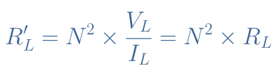
The slope of the load line will be given by -1/R’L where R’L is the apparent load in the primary circuit.
The expression of the apparent load is defined such as R’L=VC/IC. From Equation 4, we know that VC=N×VL and IC=IL/N. It comes therefore, that the apparent load is given by :
As shown in Figure 2 for the basic CEAA, we can decompose for the transformer-coupled CEAA the output signals in a DC component (Vsupply,IC0) and an AC component (VAC,IAC).
Having all of this information in mind, the diagram of power distribution of the transformer-coupled CEAA is presented in Figure 5 :
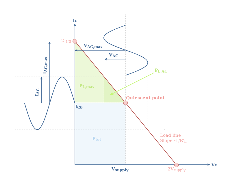
When comparing Figures 3 and 5, we can clearly see that in the case of a transformer-coupled configuration, the proportion of the light green area representing the useful absorbed power for the amplification process is much larger.
The efficiency is maximized when VAC and IAC are maximized. In this case, VAC,max=Vsupply and IAC,max=IC0. The maximum efficiency ηmax of a transformer-coupled CEAA is therefore given by :
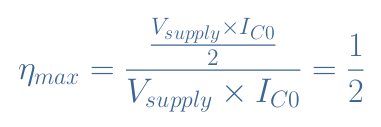
The efficiency of this configuration is improved by a factor of 2 when compared to the basic CEAA configuration. Ideal efficiency of 50 % can thus be achieved when coupling the output stage of a Class A amplifier with a transformer.
Conclusion
During this tutorial we have presented in details the characteristics and possible improvements of Class A amplifiers. As a reminder to the introductory article, we have seen that Class A amplifiers are biased such as 100 % of the input signal can be used for the amplification process. Moreover, they present a rather low efficiency, but a faithful reproduction of the signal.
The core of the tutorial deals with two configurations based on a Common Emitter Amplifier structure (CEA). The first one is the most basic architecture called “basic CEAA” with the load wired between the power supply and the collector branch of the bipolar transistor. The big inconvenient of the basic CEAA is that the operating (or quiescent) point is located in (VC0,IC0), which limits as seen in Figure 3 the useful power absorbed for the amplification of the AC signal. The efficiency of a basic CEAA is therefore limited to a theoretical maximum of 25 %.
The second architecture called “transformer-coupled CEAA” overcomes this problem by decoupling the load and the collector branch with the use of a transformer. The operating point is shifted to (Vsupply,IC0), allowing to increase the useful absorbed power with keeping the total supplied power unchanged as highlighted in Figure 5. The efficiency of a transformer-coupled CEAA is enhanced by a factor 2 reaching a theoretical maximum of 50 %.
Despite the improvement of efficiency brought by the transformer, it also brings some inconvenient. Indeed, the transformer induces an extra cost and an extra weight to the final product. The size of a transformer can also be restrictive for packaging purposes. Finally, extra complexity and cost need to be taken into consideration to protect the transistors against possible damages caused by back electromotive forces from the inductance.
In the next article of this series of amplifier classes, we will present in detail the Class B amplification that can overcome the low efficiency of Class A amplifiers.
Please follow and like us:
Subscribe
Login
0 Comments