A multi-protocol SoC for ultra low-power wireless applications
Author: Maurizio Di Paolo Emilio The nRF52840 SoC of Nordic Semiconductor is based on a 32-bit ARM Cortex-M4F CPU running at 64 MHz with flash and RAM integrated on chip. Ultra low-power wireless applications can use this advanced multi-protocol SoC with different communication protocols.
Author: Maurizio Di Paolo Emilio
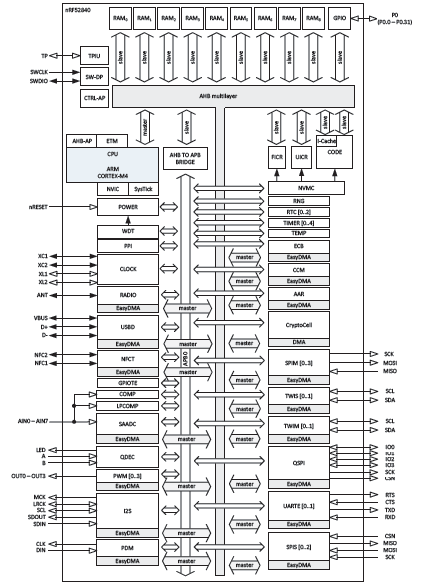
The nRF52840 SoC of Nordic Semiconductor is based on a 32-bit ARM Cortex-M4F CPU running at 64 MHz with flash and RAM integrated on chip. Ultra low-power wireless applications can use this advanced multi-protocol SoC with different communication protocols. The 2.4 GHz transceiver supports Bluetooth low energy (Bluetooth 5), 802.15.4, ANT and proprietary protocols. The transceiver also supports high resolution RSSI measurement and automated processes to reduce CPU load. Moreover, EasyDMA for direct data memory access and packet assembly provides full support for hardware (figure 1). The device maintains the compatibility with existing products such as nRF52, nRF51 and nRF24 series.
Bluetooth 5 and SoC
Bluetooth 5 (500kbs e 125kbs) is the latest version of the well-known wireless technology. It increases the range of four times and the throughput of eight times, making this technology much more suitable for ultra low-power wireless applications such as wearable, Smart Home and more generally for Internet-related applications (IoT, IIoT). The ultra low power consumption of the Bluetooth 5 protocol facilitates high performance, advertising extension and modulation schemes.
nRF52840 SoC uses power management resources to maximize job processes and achieve an optimal energy efficiency. The power supply ranges between 1.7V and 5.5V ensures a wide choice of batteries. In addition, SoC can also work with USB direct power supply without external regulators. Especially relevant, all devices have automatic clock management with adaptive features to maintain minimal power consumption.
Features:
- multi-protocol SoC
- 32-bit ARM Cortex-M4F Processor
- 1.7v to 5.5v operation
- 1MB flash + 256kB RAM
- Bluetooth 5 support for long range and high throughput
- 802.15.4 radio support
- On-chip NFC
- PPI –Programmable Peripheral Interconnect
- Automated power management system with automatic power management of each peripheral
- Configurable I/O mapping for analog and digital I/O
- 48 x GPIO
- 1 x QSPI
- 4 x Master/Slave SPI
- 2 x Two-wire interface (I²C)
- I²S interface
- 2 x UART
- 4 x PWM
- USB 2.0 controller
- ARM TrustZone CryptoCell-310 Cryptographic and security module
- AES 128-bit ECB/CCM/AAR hardware accelerator
- Digital microphone interface (PDM)
- Quadrature decoder
- 12-bit ADC
- Low power comparator
- On-chip 50Ω balun
- On-air compatible with nRF52, nRF51 and nRF24 Series
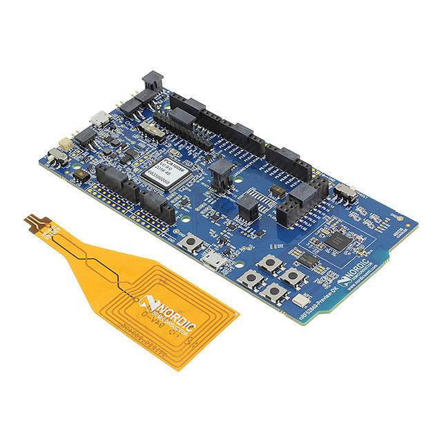
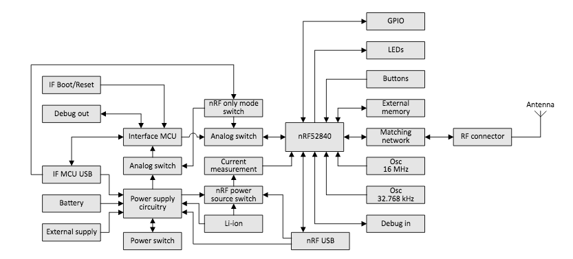
Development kit
The NRF52840-PDK is a versatile development kit based on nRF52840 SoC for the development of projects by using Bluetooth Low Energy, ANT, 802.15.4, and proprietary 2.4GHz protocols. Moreover, It is also hardware-compatible with the Arduino Uno R3 standard, allowing to use third-party compatible shields. Adding an NFC antenna, the kit enables the NFC tag feature (figure 2 and 3).