REAL3™ Time-of-Flight image sensor: fourth generation with HVGA resolution
Infineon Technologies AG is presenting the fourth generation of its REAL3™ image sensor IRS2771C at Mobile World Congress 2019 in Barcelona, Spain. The 3D Time-of-Flight (ToF) single chip is especially designed to meet the requirements of the mobile consumer device market and, in particular, demand for higher resolutions with small lenses.
Infineon Technologies AG is presenting the fourth generation of its REAL3™ image sensor IRS2771C at Mobile World Congress 2019 in Barcelona, Spain. The 3D Time-of-Flight (ToF) single chip is especially designed to meet the requirements of the mobile consumer device market and, in particular, demand for higher resolutions with small lenses. The wide range of use cases includes secure user authentication like face or hand recognition to unlock the device and confirm payments. In addition, the 3D ToF chip enhances augmented reality, morphing and photo (e.g. bokeh) effects and can be used to scan a room.
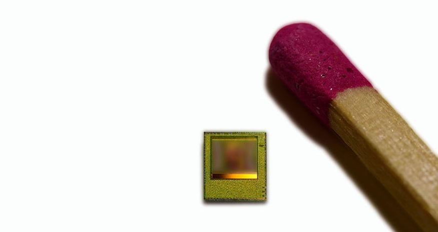
Measuring only 4.6 x 5 mm, the image sensor features a 150 k (448 x 336) pixel output that comes close to the HVGA standard resolution. This makes the resolution four times higher than that of most ToF solutions on the market today. The pixel array is highly sensitive to 940 nm infrared light and provides unbeaten outdoor performance. This is enabled by the patented Suppression of Background Illumination (SBI) circuitry in every pixel. Due to its high level of integration, each IRS2771C image sensor is essentially a miniature single-chip ToF camera. This dramatically reduces the overall bill of materials and the actual size of the camera module without compromising on performance and keeping power consumption to a minimum.
Market-leading robustness and energy efficiency
Its robustness against ambient light and its energy efficiency make this imager unparalleled in the market,” says Philipp von Schierstaedt, Vice President and responsible for Infineon’s RF & Sensors business. “With the new image sensor generation, Infineon can further extend its leading position. Every device manufacturer can increase the value of their devices with the new REAL3 chip, while customizing the design and speeding up time to market
Through its long-standing partnership with pmdtechnologies, Infineon has gained profound expertise in algorithms for processed 3D point clouds (a set of data points in space produced by 3D scanning). Reaching beyond Infineon’s hardware expertise, customers can thus expect a comprehensive offering including tooling and software. “The fruitful collaboration has proven that best-in-class 3D ToF systems are only achievable by designing the depth sensing system from scratch – from cutting edge ToF pixel, imager and module design to advanced signal processing,” said Bernd Buxbaum, CEO of pmdtechnologies.
Our customers leverage pmd’s vast experience from 15 years in developing and manufacturing best-in-class 3D ToF products.
Availability
Developed in Graz, Dresden and Siegen, Infineon’s new 3D image sensor chip bundles Infineon’s expertise at its German and Austria sites. Samples of the chip will be available in March and volume production is scheduled to start in Q4 2019. More information about Infineon’s 3D image sensor family and the company’s demonstrations at Mobile World Congress 2019 is available at www.infineon.com/real3 and at www.infineon.com/MWC.


