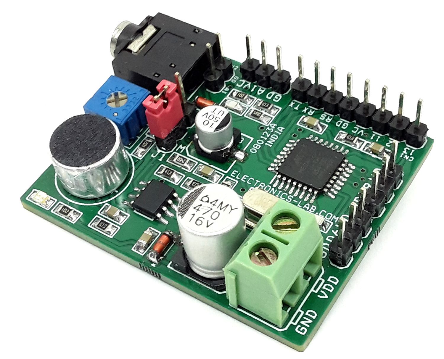
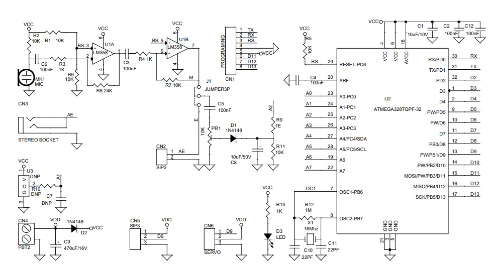
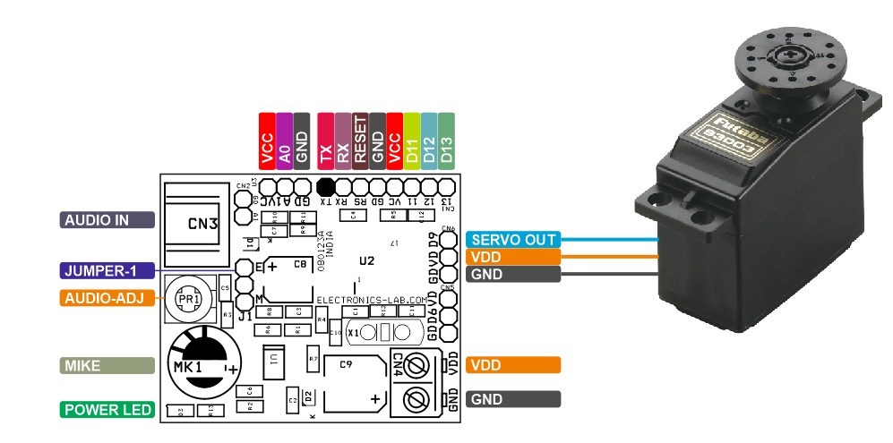
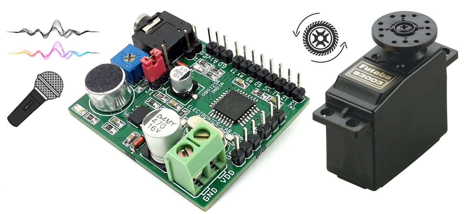
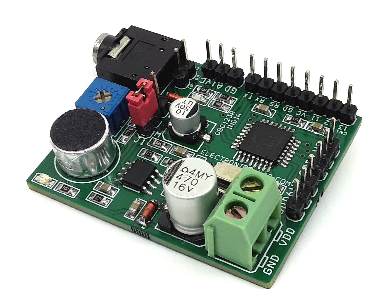
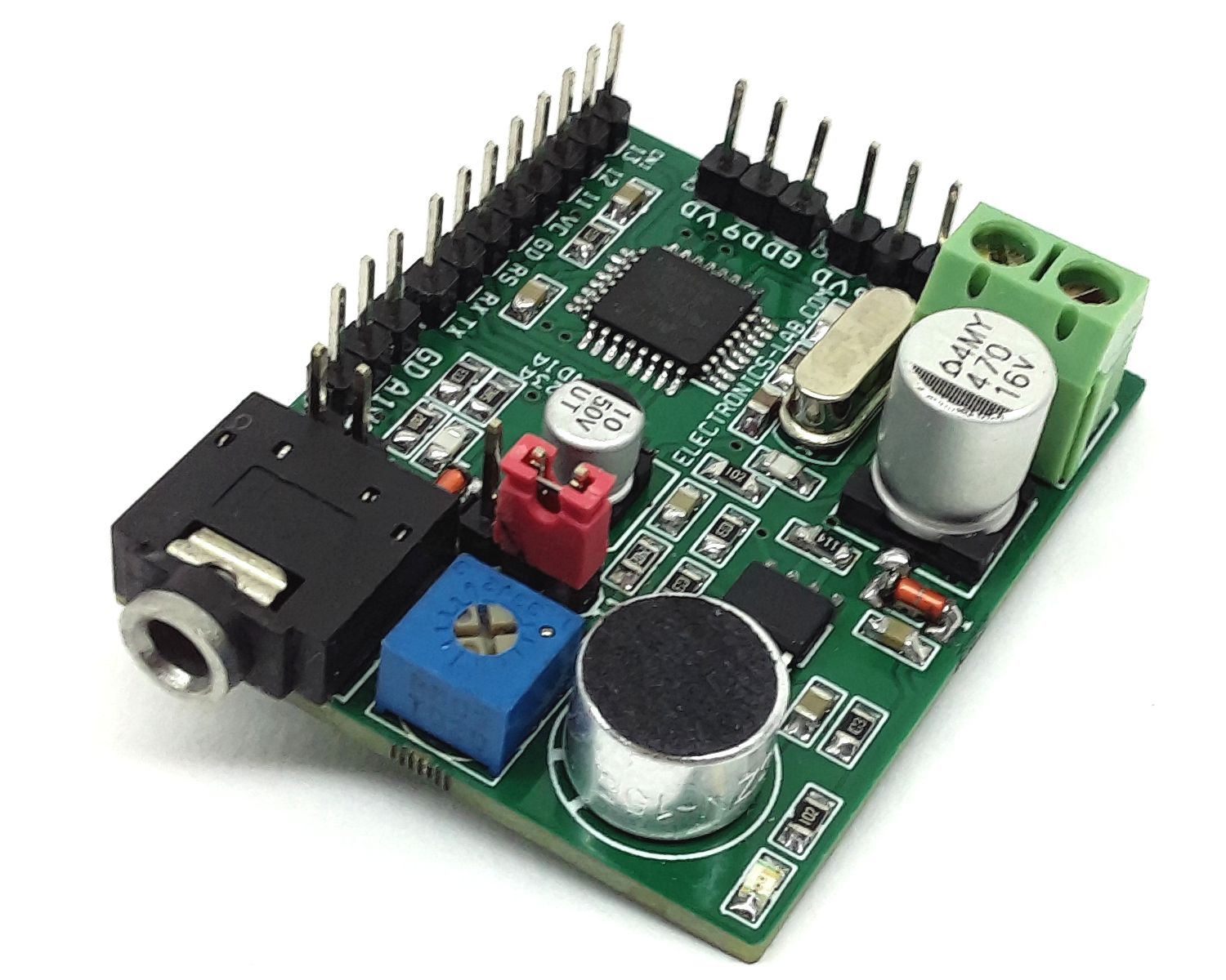
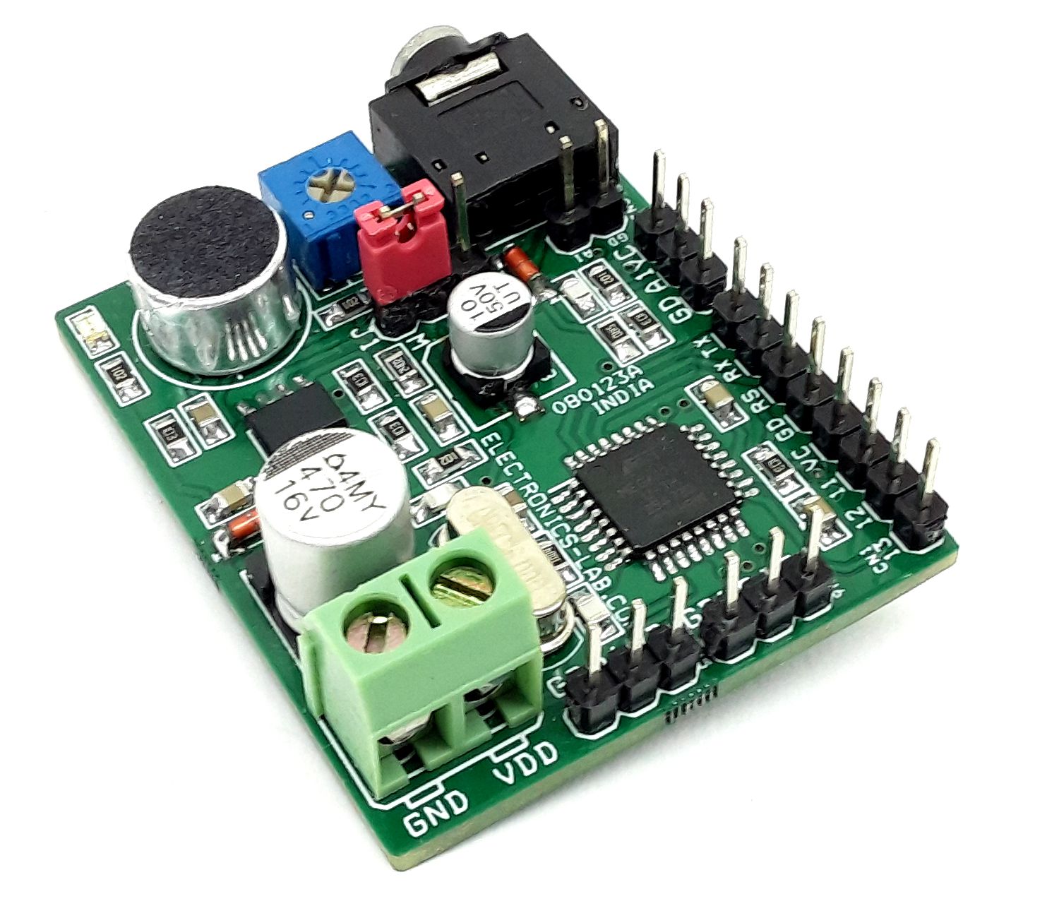
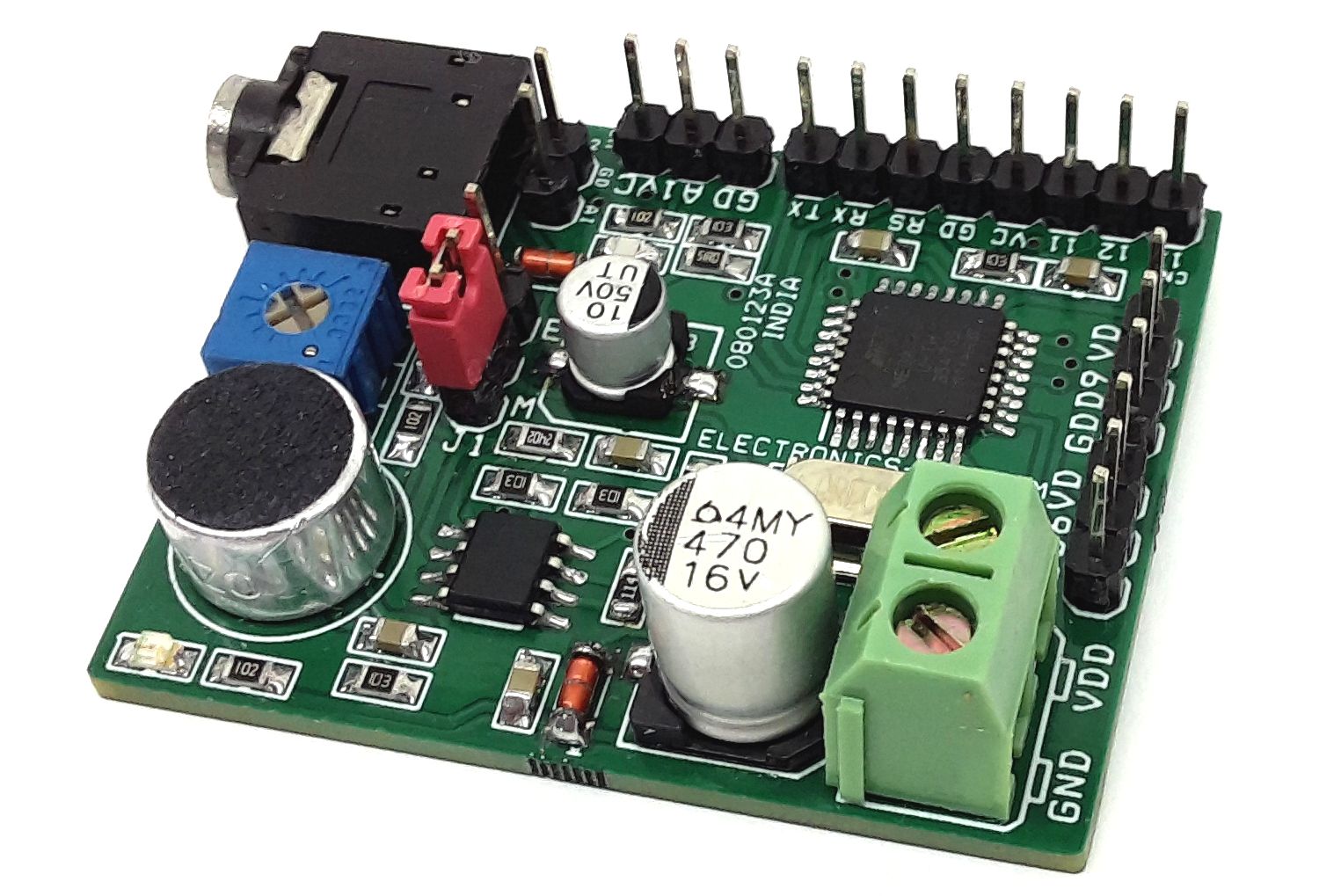
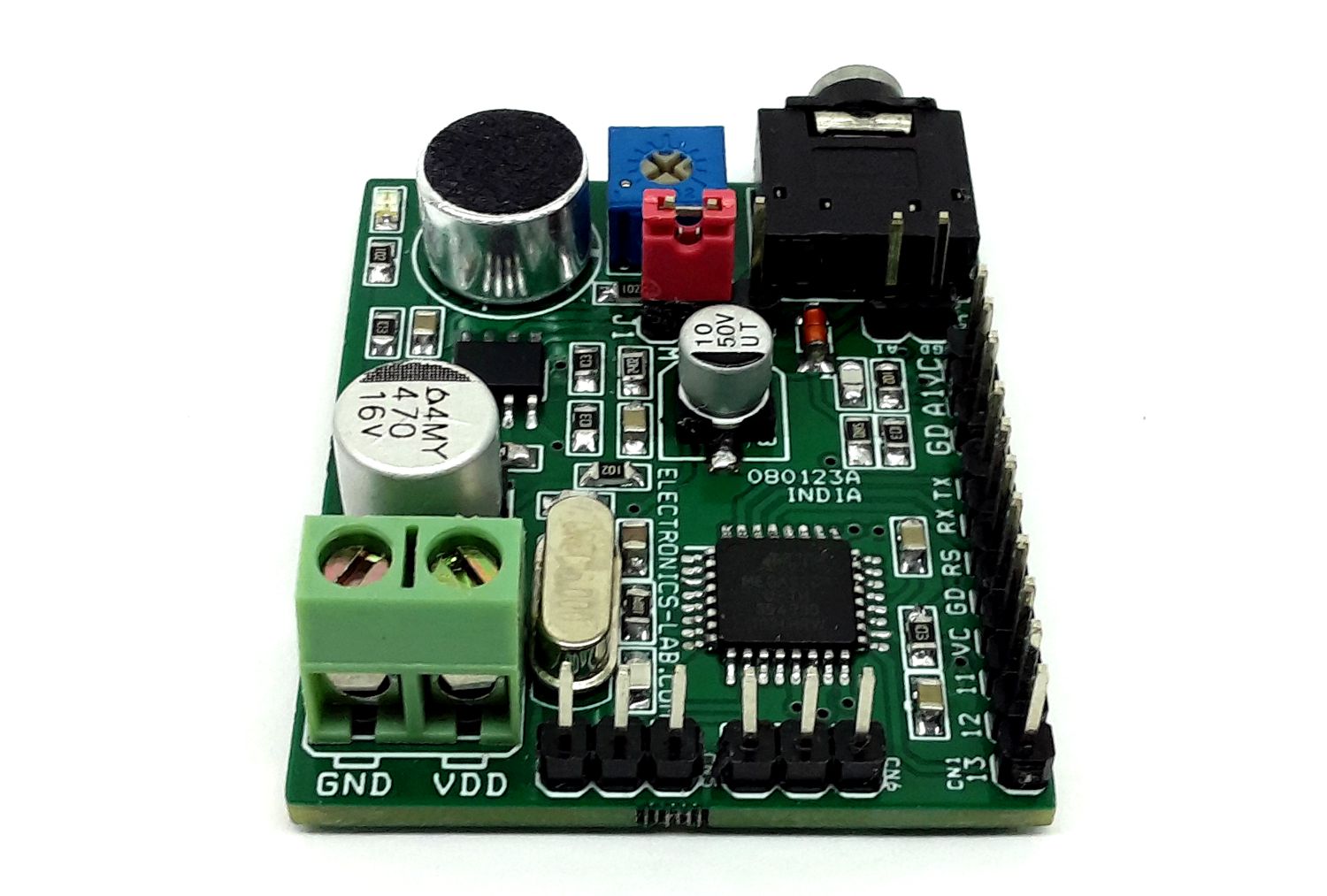
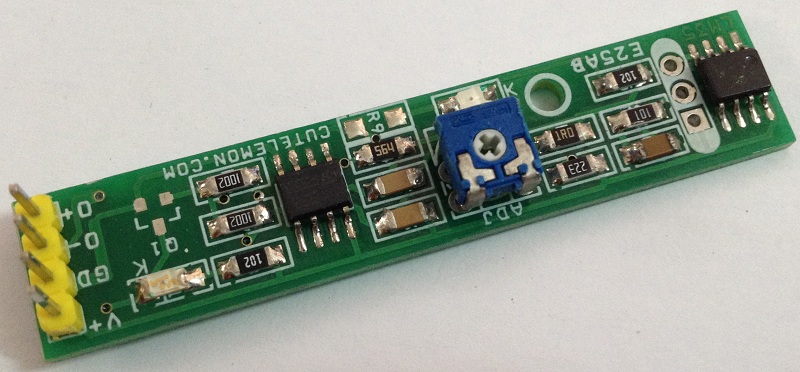
The project presented here is made for applications such as Animatronics, Puppeteer, sound-responsive toys, and robotics. The board is Arduino compatible and consists of LM358 OPAMP, ATMEGA328 microcontroller, microphone, and a few other components. The project moves the RC servo once receives any kind of sound. The rotation angle depends on the sound level, the higher the sound level the biggest the movement, in other words, the movement of the servo is proportional to the sound level. The microphone picks up the soundwave and converts it to an electrical signal, this signal is amplified by LM358 op-amp-based dual-stage amplifier, D1 helps to rectify the sinewave into DC, and C8 works as a filter capacitor that smooths the DC voltage. ATmega328 microcontroller converts this DC voltage into a suitable RC PWM signal.
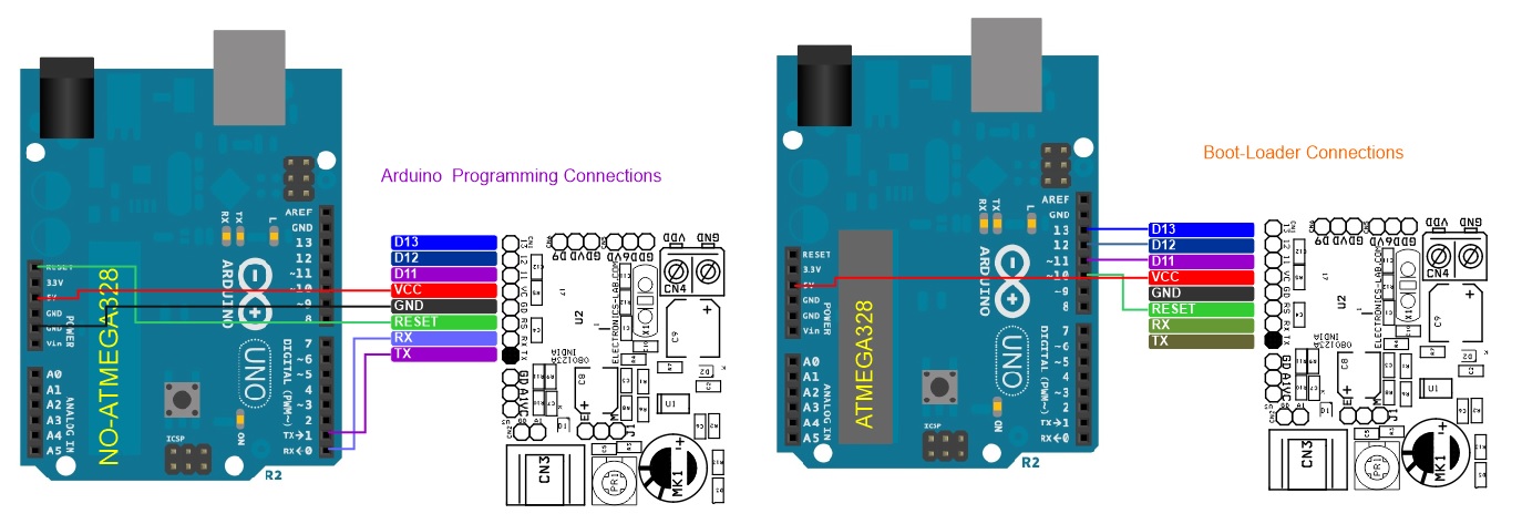
The project is Arduino compatible and an onboard connector is provided for the boot-loader and Arduino IDE programming. Arduino code is available as a download, and Atmega328 chips need to be programmed with a bootloader before uploading the code. Users may modify the code as per requirement. More information on burning the bootloader is here: https://www.arduino.cc/en/Tutorial/BuiltInExamples/ArduinoToBreadboard
Direct Audio Input: The audio input signal should not exceed 5V, It is important to maintain the input audio signal at this maximum level, otherwise it can damage the ADC of ATMEGA328.
Features
Supply 5V to 6V DC (Battery Power Advisable)
RC Servo Movement 180 Degrees with Loud sound
Direct Sound Input Facility Using 3.5MM RC Jack
On Board Jumper Selection for Micro-Phone Audio or External Audio Signal
On Board Trimmer Potentiometer to Adjust the Signal Sensitivity
Flexible Operation, Parameters Can be Changed using Arduino Code
/*
 Controlling a servo position using a potentiometer (variable resistor)
 by Michal Rinott <http://people.interaction-ivrea.it/m.rinott>

 modified on 8 Nov 2013
 by Scott Fitzgerald
 http://www.arduino.cc/en/Tutorial/Knob
*/

#include <Servo.h>

Servo myservo;  // create servo object to control a servo

int potpin = A2;  // analog pin used to connect the potentiometer
int val;    // variable to read the value from the analog pin

void setup() {
  myservo.attach(6);  // attaches the servo on pin 6 to the servo object
}

void loop() {
  val = analogRead(potpin);            // reads the value of the potentiometer (value between 0 and 60)
  val = map(val, 0, 60, 0, 180);     // scale it for use with the servo (value between 0 and 180)
  myservo.write(val);                  // sets the servo position according to the scaled value
  delay(15);                           // waits for the servo to get there
}
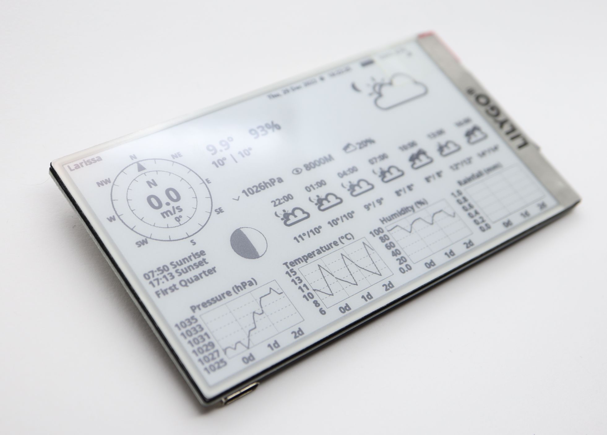
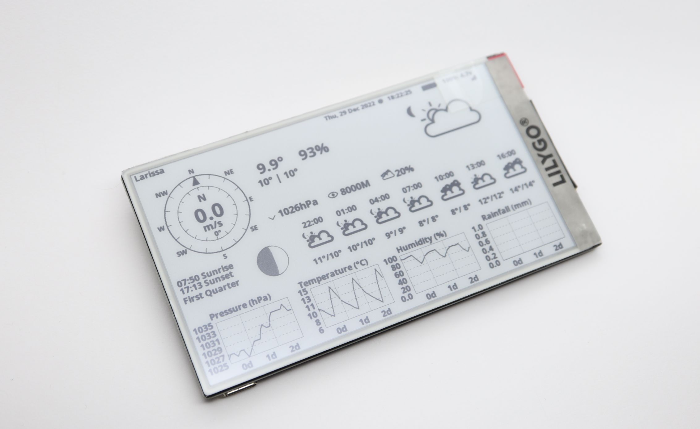
The LILYGO T5 4.7 inchE-Paper ESP32 Development Board is an exciting 4.7″ e-paper display integrated with an ESP32 WiFi/Bluetooth module. The board’s processor is ESP32-WROVER-E with 16MB of FLASH memory and 8MB of PSRAM. The ESP32 module supports Wi-Fi 802.11 b/g/n and Bluetooth V4.2+BLE and can easily be programmed with Arduino IDE, VS Code, or ESP-IDF. The board can be purchased on Alliexpress for 38.33 EUR + shipping or Tindie for 28.13 + shipping. This display is ideal for building a weather station that will fetch weather data from OpenWeatherMap via simple API usage. So in this tutorial, we will follow the steps to make a weather station like the photo above. We will work on a Windows PC to program the display, but the same can be done in Linux or Mac OS.
Specifications
MCU: ESP32-WROVER-E (ESP32-D0WDQ6 V3)
FLASH: 16MB
PRAM: 8MB
USB to TTL: CP2104
Connectivity: Wi-Fi 802.11 b/g/n & Bluetooth V4.2+BLE
Onboard functions: Buttons: IO39+IO34+IO35+IO0, Battery Power Detection
Power Supply: 18650 Battery or 3.7V lithium Battery (PH 2.0 pitch)
First of all, we will need to install the USB to Serial (CH343) Drivers if we don’t have this done previously. Depending on your Windows version you will need:
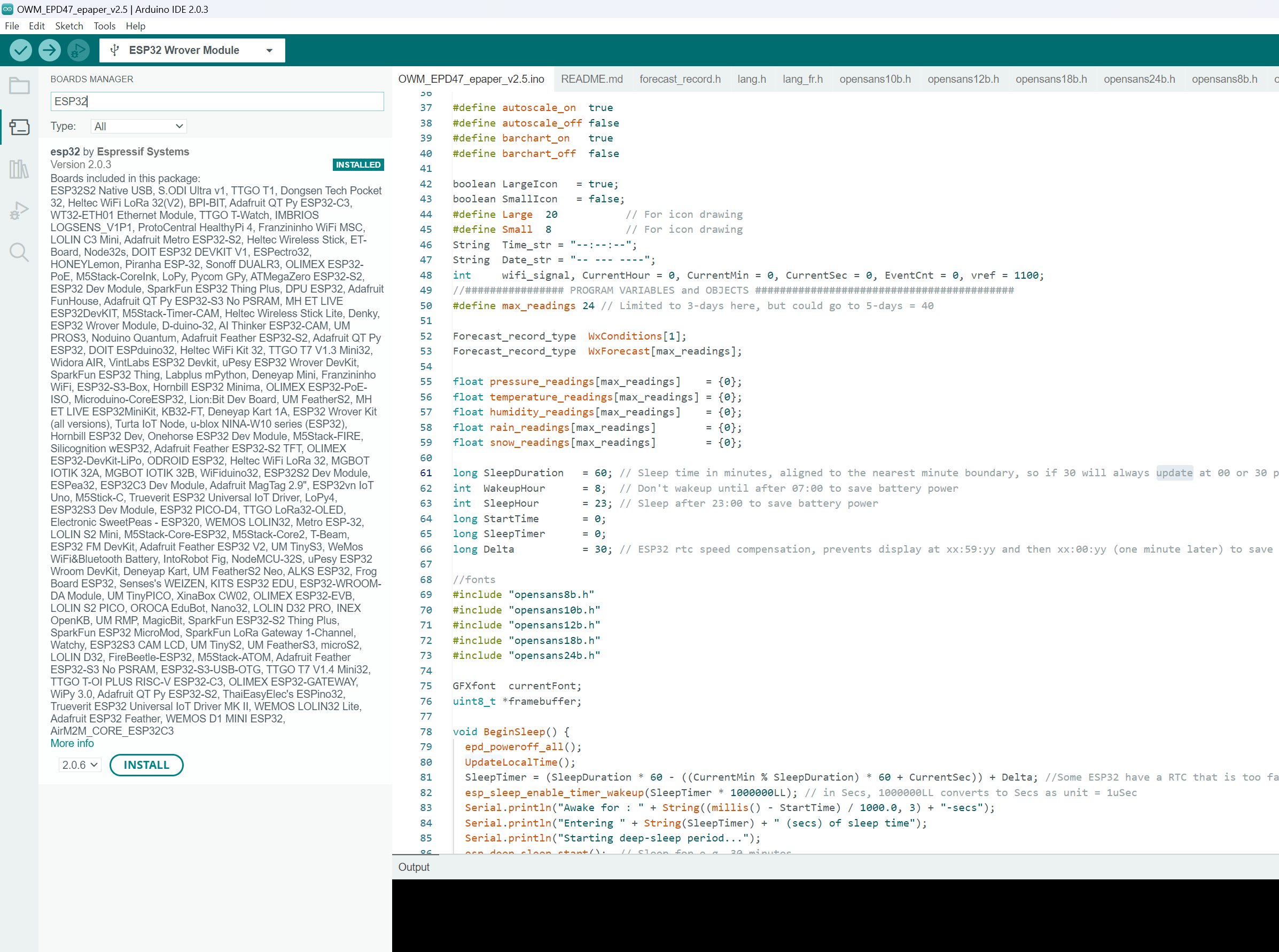
Next click Tools, and select Boards: -> Boards Manager . It will open the left pane with a list of boards. Type ESP32 into the search field. Find ESP32 by Espressif Systems, and click Install.
Preparing the Code
Download LilyGo-EPD47 library to the C:\Users\YOUR_USERNAME\Documents\Arduino\libraries folder on your system:
Download and extract LilyGo-EPD-4-7-OWM-Weather-Display to your directory with Arduino projects. This directory is normally located in C:\Users\YOUR_USERNAME\Documents\Arduino.
The project folder name should match the name of the source code file (OWM_EPD47_epaper_v2.5). This is done to avoid the unnecessary step of moving the files later.
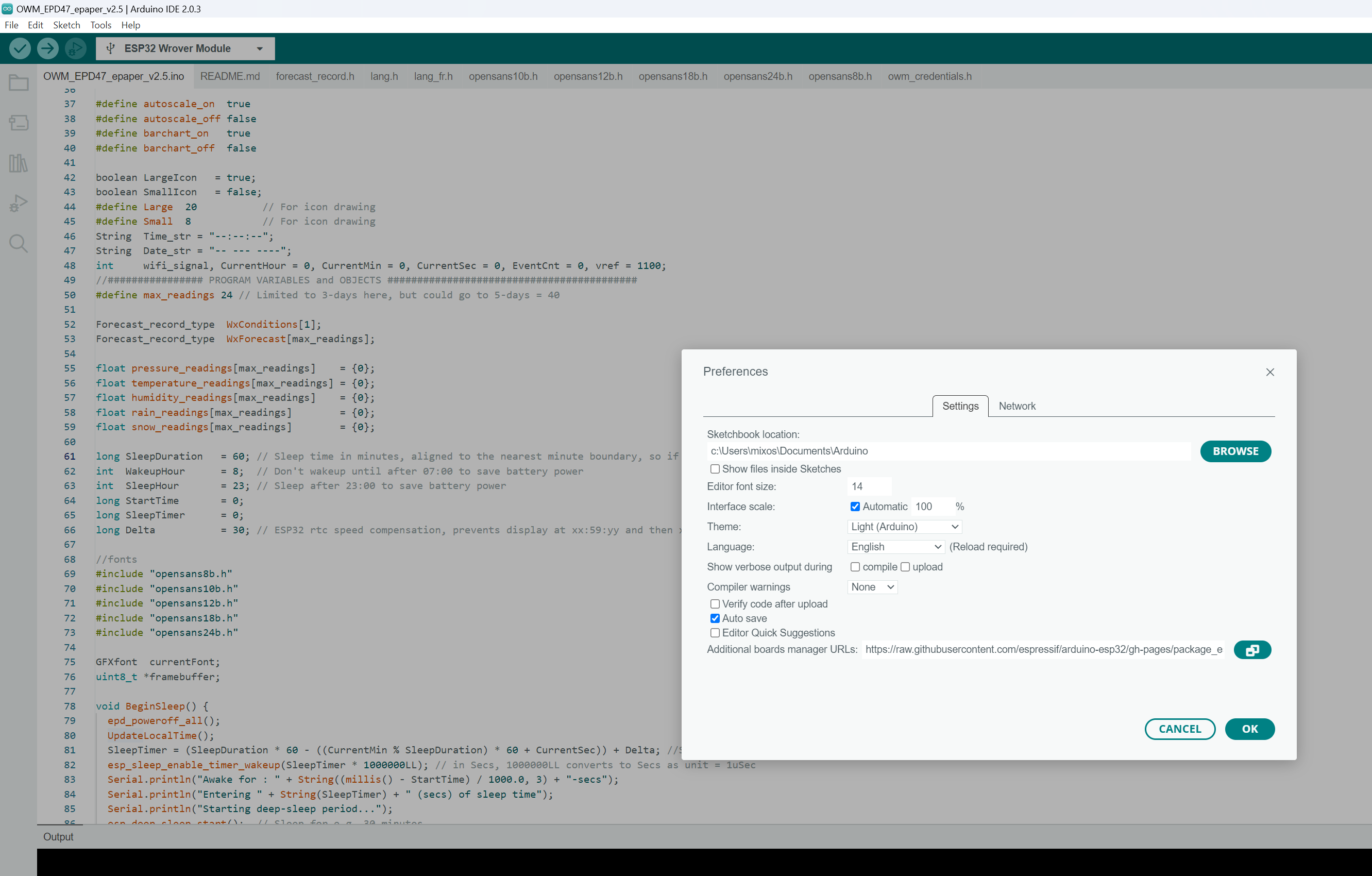
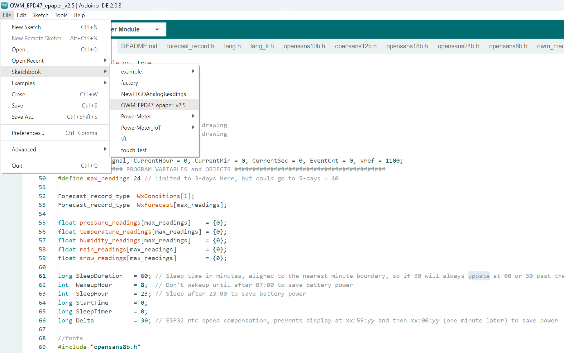
Open Arduino IDE 2.0, click File, -> Sketchbook, -> OWM_EPD47_epaper_v2.5.
The sketch requires ArduinoJson Library to successfully build.
Click Tools, ->Manage libraries. The pane with Library Manager will open, then type ArduinoJson into the search field. Find ArduinoJson by Benoit Blanchon, click Install.
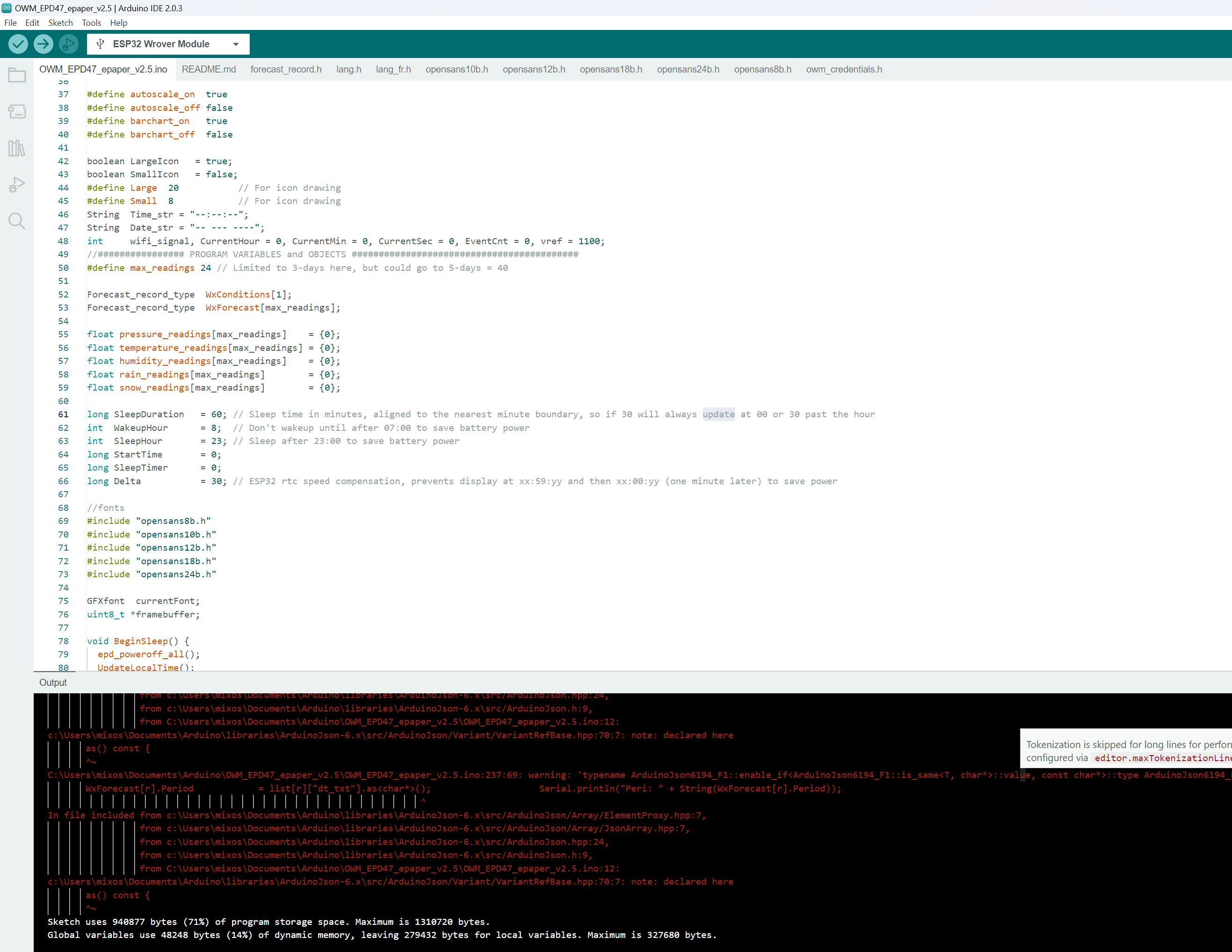
Then click the tick button on the top menu to compile the code. If everything is successful it should show:
Once you verify that the code is compiled you can move on to the next step.
Configuring Parameters
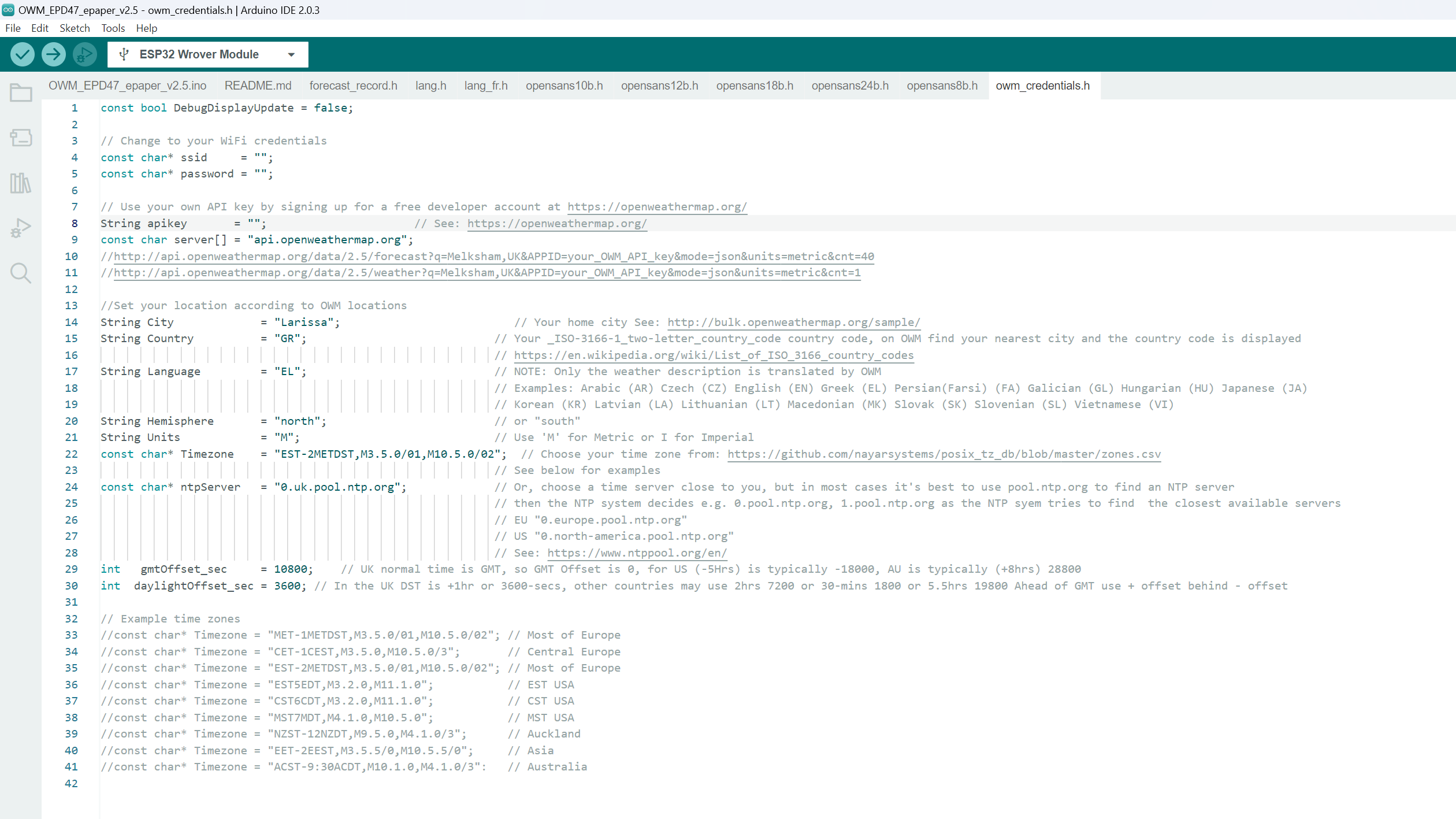
Open the file owm_credentials.h and configure ssid, password, apikey, City, and Country.
The project is fetching data from openweathermap.org so you will need to create a new free account in order to get API key.
Power Saving
The project code supports power saving, so if you’re flashing in the early before 08.00 or after 23.00, you might notice that nothing appears on the display.
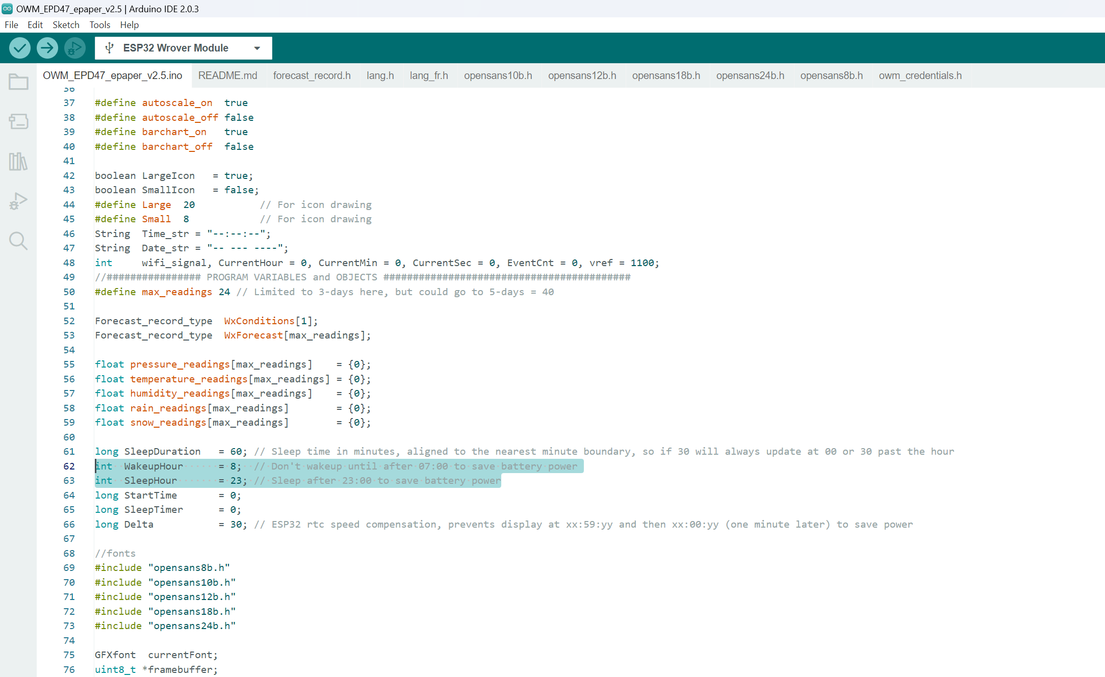
To change the power-saving options open file OWM_EPD47_epaper_v2.5.ino and change WakeupHour and SleepHour to a value that suits your schedule.
Uploading the Code
Connect the LilyGO T5 4.7-inch e-paper display to your PC-> Select the board from the dropdown in the toolbar. Search for the ESP32 Wrover module and click Ok.
Click the Upload button.
If the flashing is successful, your weather will be displayed on the e-paper like the photos below.
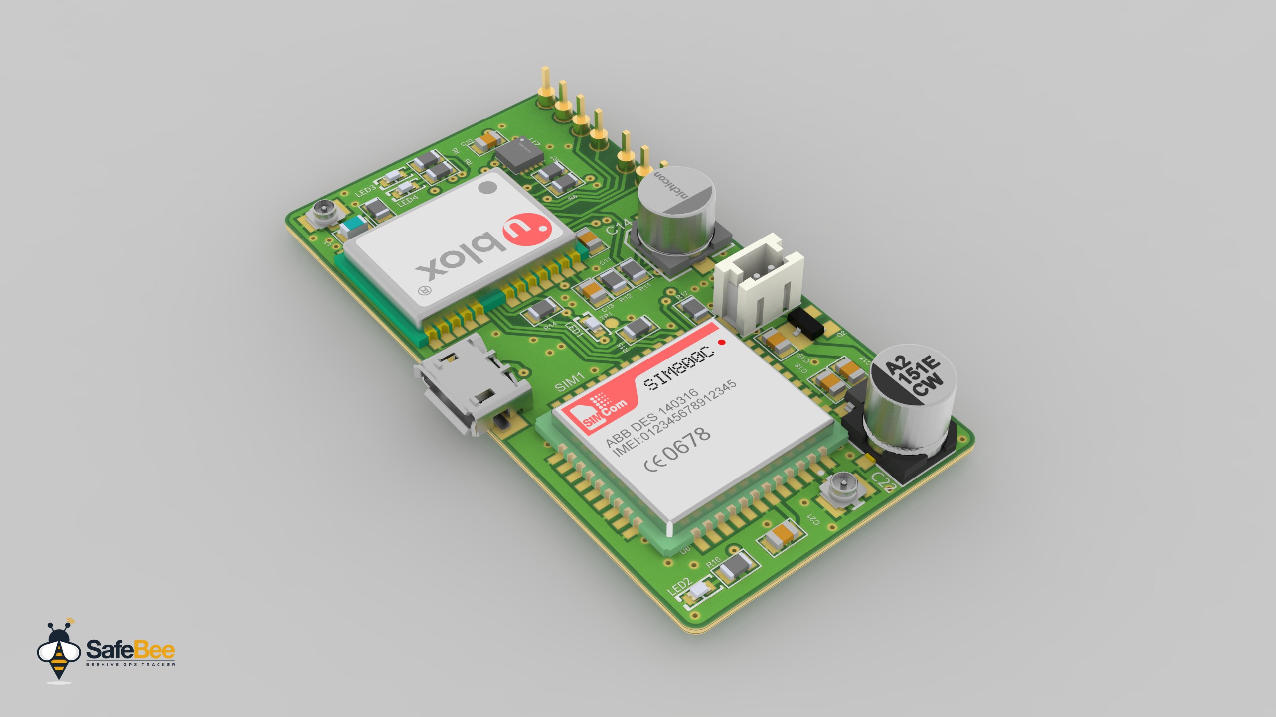
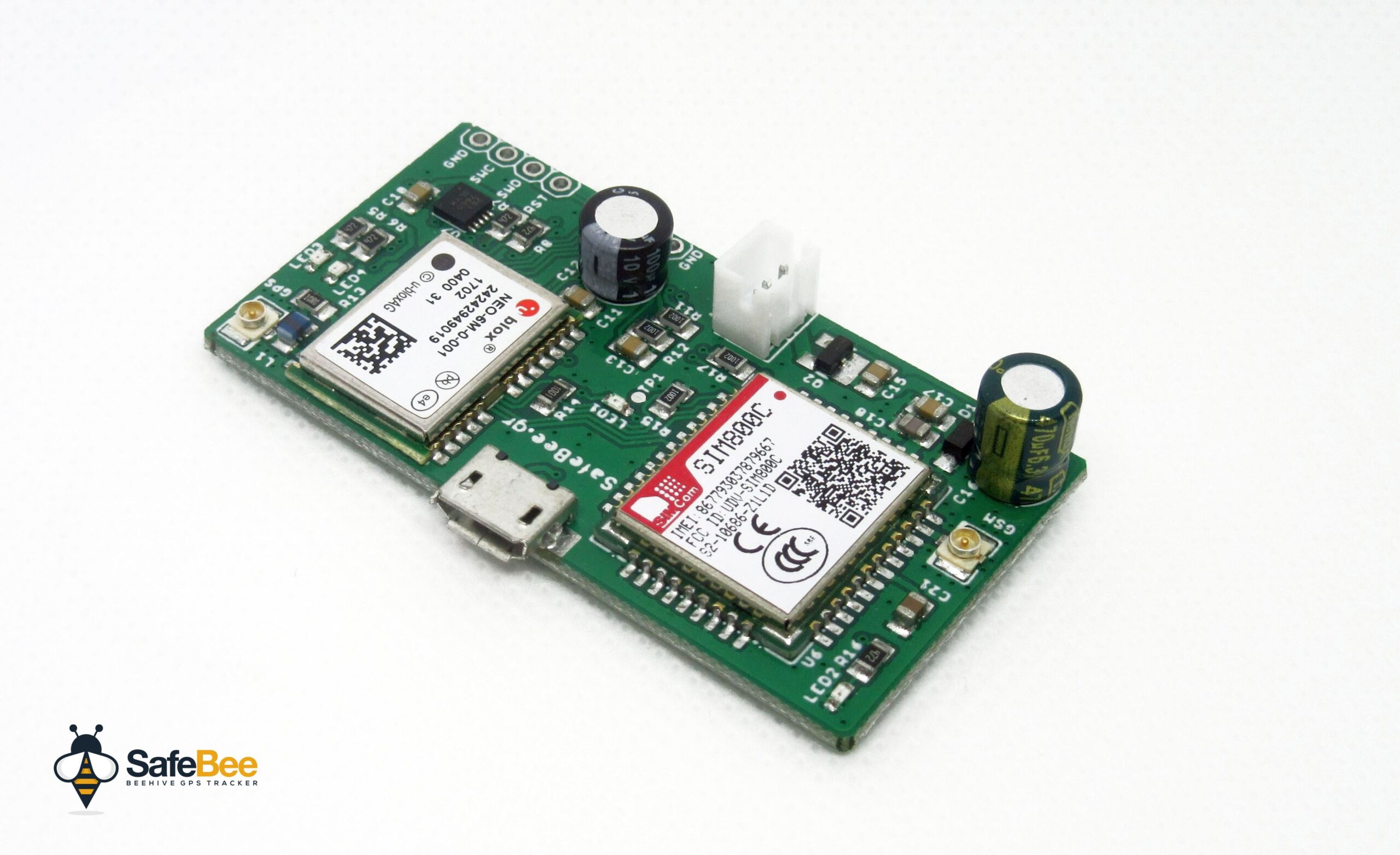
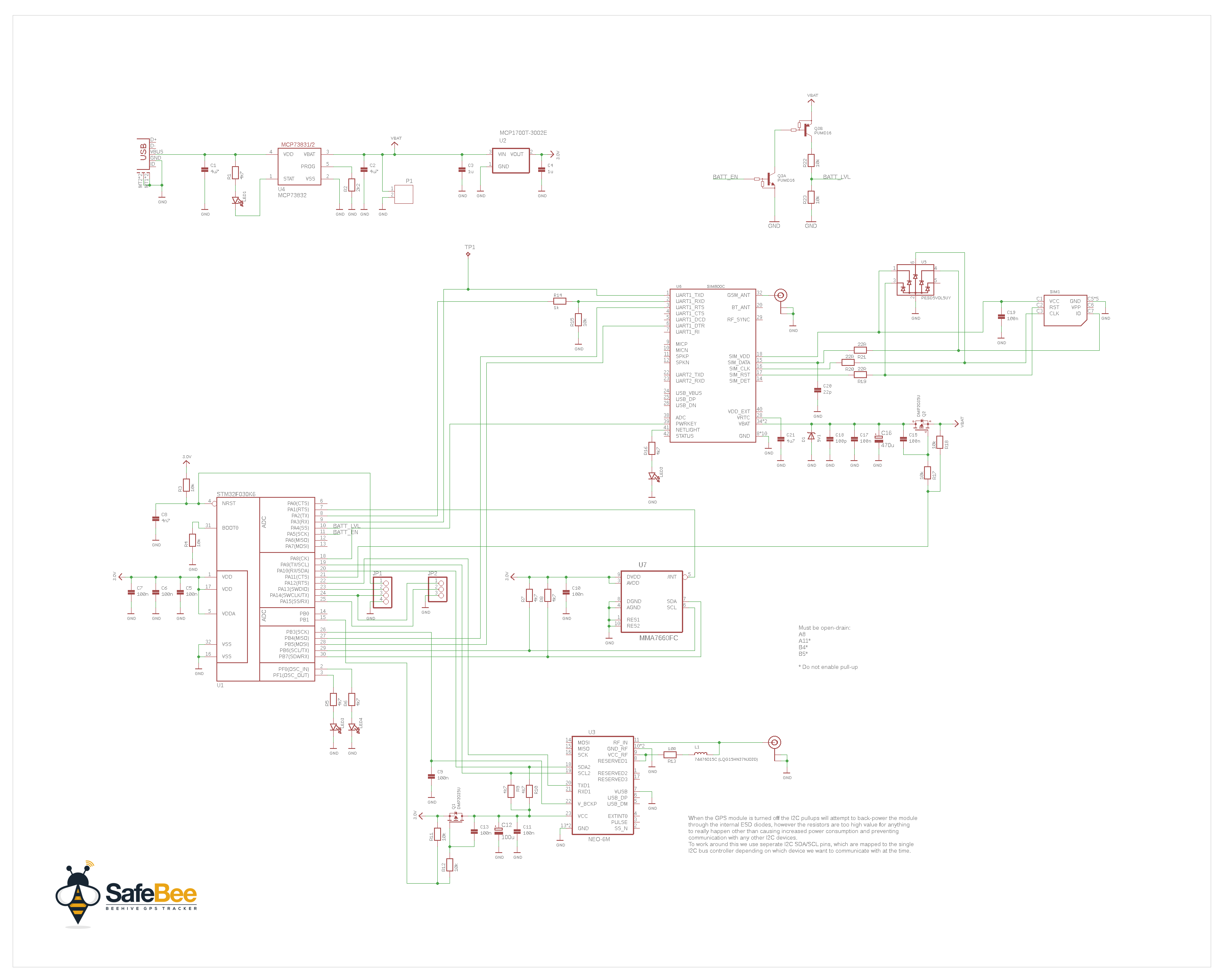
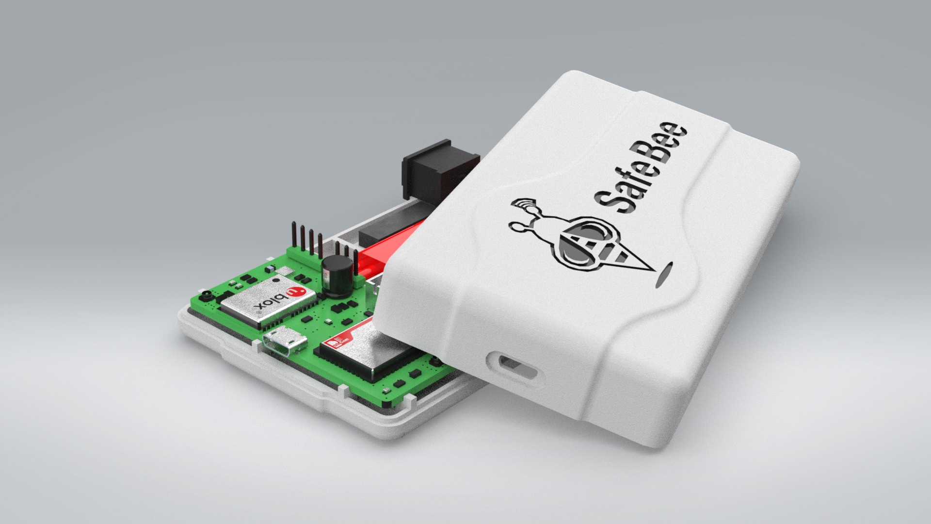
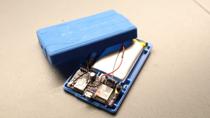
This is an original design of a GPS tracker designed on Elab and it is intended to be used as a security device for beehives, but it is not limited to this. It can be used everywhere a motion-activated GPS tracker is needed, like your car, bike, or even your boat. It is a GPS tracker controlled by simple SMS commands and designed for reliability,low power consumption, and easeof use. It features a MEMS accelerometer that is used to intelligently detect movement and once triggered it will power on the GPS module and will try to acquire the current coordinates. The location details will be transmitted to the owner’s smartphone via a simple SMS and then follow update the coordinates at predefined intervals.
Key Features:
Remote management via simple SMS commands
High reliability – no need to babysit the tracker due to crashes and resets
Long battery life – over 1 year standby on a single charge (2500mAh battery)
3-axis high-sensitivity MEMS Accelerometer
Intelligent Triggering – it will not be triggered by accidental movement
Selectable Trigger Sensitivity Level
Description of Operation
The tracker has 3 main modes of operation, detailed below:
Standby
Ready
Tracking
Standby mode
In standby mode, the GSM and GPS modules are powered down and the microcontroller is in sleep mode, resulting in a current draw of approximately 70uA, mainly by the accelerometer (MMA7660). The accelerometer is used to detect movement caused by a possible thief. If the accelerometer is triggered 1 or 2 or 3 times (depending on the sensitivity level) inside of a 60-second window then the device will enter tracking mode. While in standby mode the tracker will also enter ready mode approximately every 12 hours, triggered by the microcontroller’s internal RTC. This is to check for incoming commands and battery status etc.
Ready mode
The ready mode is entered by the microcontroller’s internal RTC and when the tracker is first powered on. In this mode, the tracker will power up the GSM module and wait for any SMSs to come in and process them. The tracker will stay in ready mode for 5 minutes before returning to standby mode unless an SMS command has instructed the device to enter tracking mode (BEE+TRIGGER).
Tracking mode
Tracking mode is entered when manually instructed to by the BEE+TRIGGER command or after the accelerometer triggers (1 or 2 or 3 movements detect depending on sensitivity level) within a 60-second window, from either standby or ready modes. In tracking mode, the tracker will power up both the GSM and GPS modules and begin to send tracking alert SMSs to the number configured by the BEE+NUMBER command. The device will continue to stay in tracking mode until the BEE+CLEAR command is received or while the accelerometer is detecting movement and/or the GPS module has a lock and the speed is greater than 10KPH. If neither of these conditions is met for 6 minutes then the tracker will send a tracking stopped SMS and return to standby mode, or ready mode if the RTC was triggered within the last 5 minutes.
Power up and Battery Status
In ready and tracking modes if the battery voltage falls below the threshold voltage (3650mV default) then a low battery alert SMS will be sent to the number configured by BEE+NUMBER. Approximately every 30 days (60 RTC triggers) an automated status SMS is also sent to the number configured by BEE+NUMBER.
When power is first applied to the device the tracker will be in ready mode and it will check for incoming SMS and then go to sleep. This is the ideal time to configure the tracker with the BEE+NUMBER number. This is the number that tracking messages, monthly status reports, and low battery alerts will be sent. The phone number is stored in the microcontroller’s FLASH memory and it will be permanently saved, even if battery power is removed. At power-up, the tracker will send a status SMS and also ignore any movement detected by the accelerometer for the first 60 seconds.
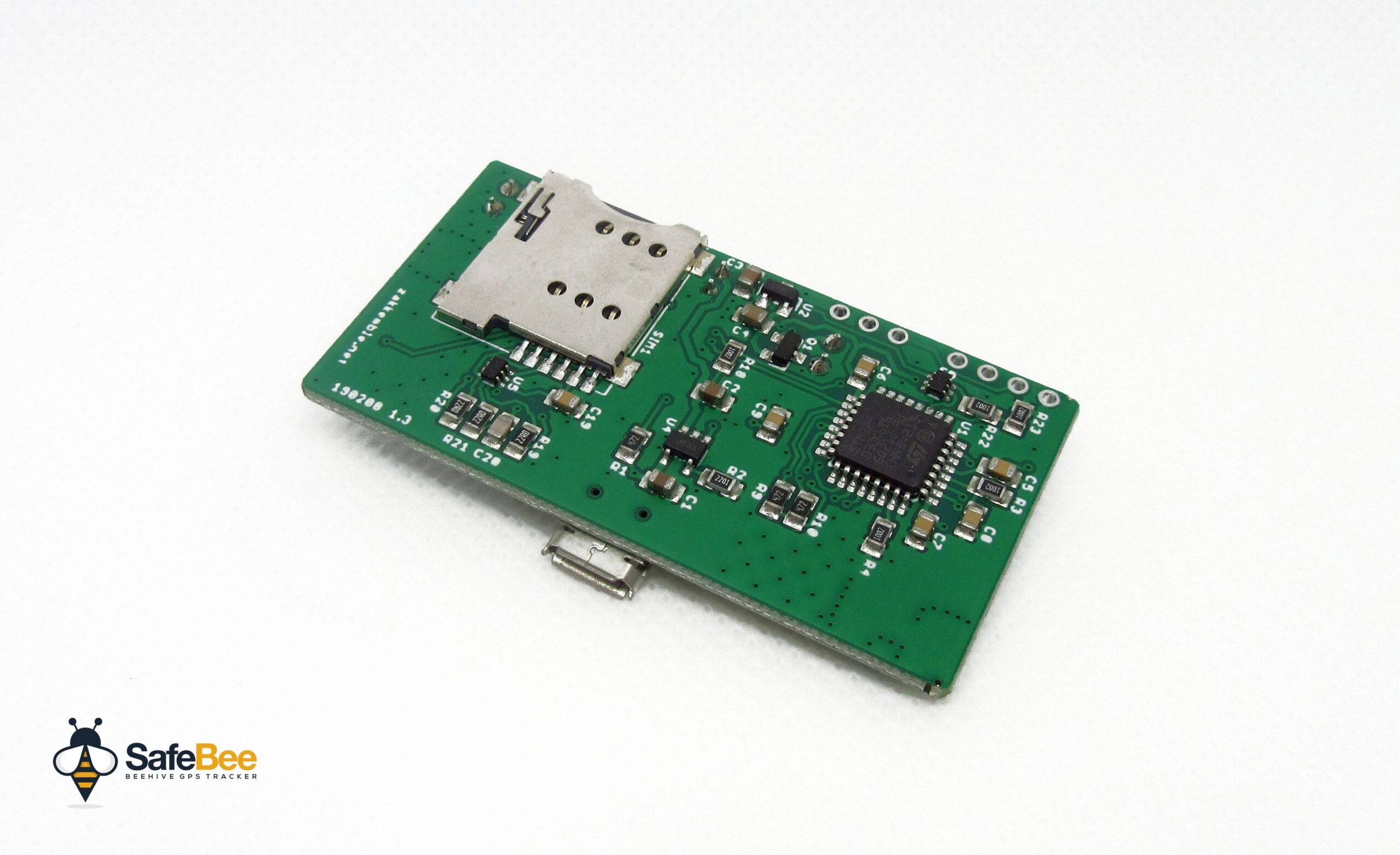
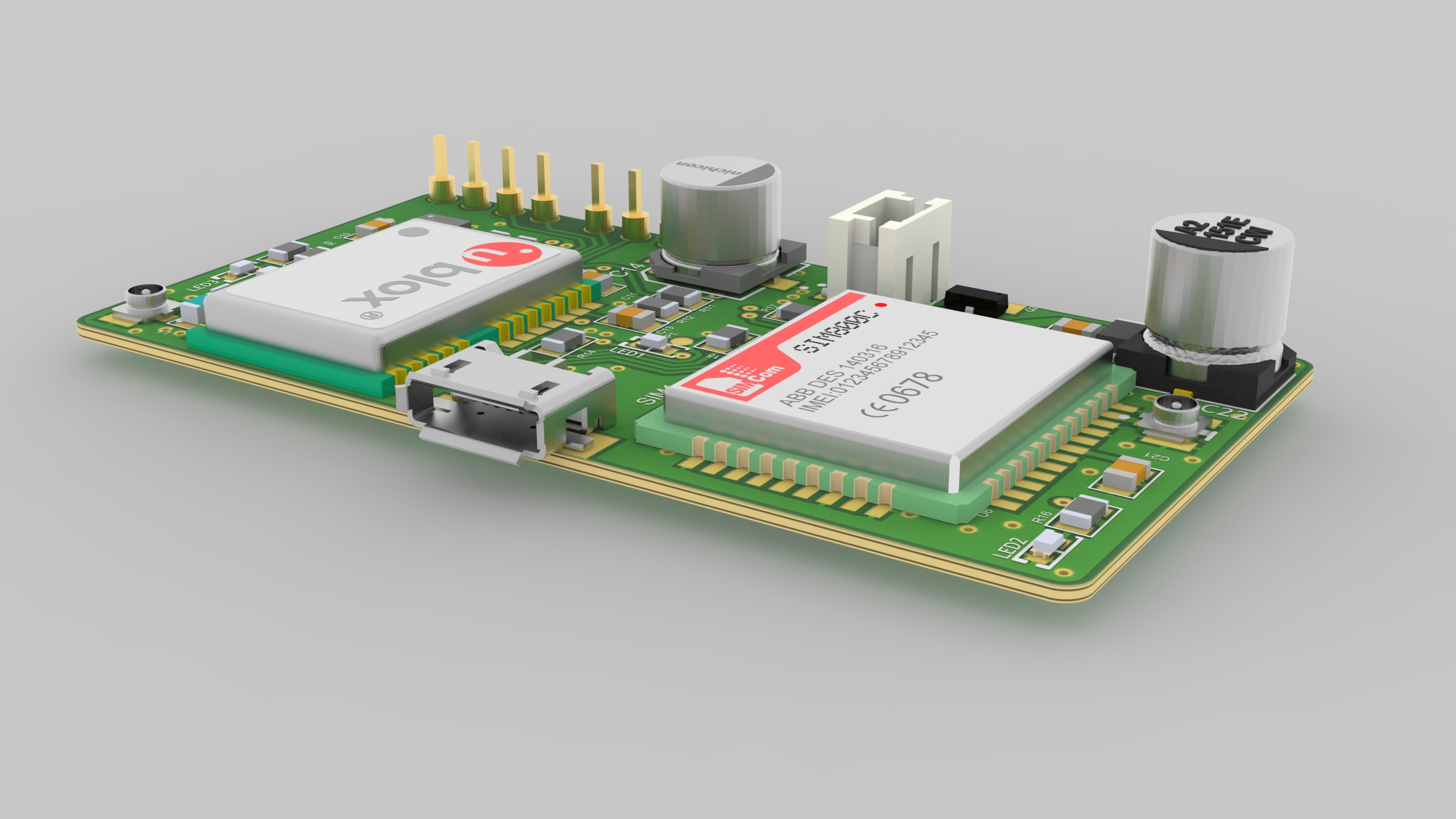
The Hardware
Hover images for details
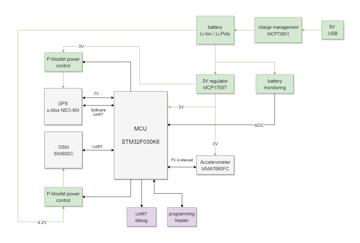
Block Diagram
MCU
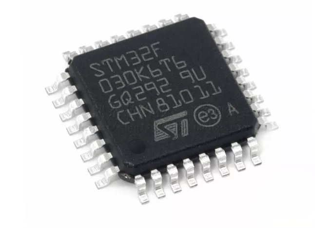
STM32F030K6
The tracker uses an ST STM32F030K6 microcontroller (ARM Cortex-M0, 32-bit RISC core), with 32KB of flash, and 4KB of RAM, and operates at up to 48MHz. The STM32F030K6 microcontroller operates in the -40 to +85 °C temperature range from a 2.4 to 3.6V power supply. A comprehensive set of power-saving modes allows the design of low-power applications. Currently, the firmware is taking roughly 24KB of flash (with debugging output enabled) and 1.7KB of RAM. The microcontroller is running at 8MHz and is supplied with 3V.
GSM module
SIMCom SIM800C
The GSM module is a SIMCom SIM800C and uses the UART bus to communicate with the MCU. The GSM module is power-gated with a P-MOSFET, controlled by the MCU, as its own low-power modes are not sufficient for this project. SIM800C supports Quad-band 850/900/1800/1900MHz, it can transmit Voice, SMS and data information with low power consumption. With a tiny size of 17.6*15.7*2.3mm, it can smoothly fit into our small board. The module is controlled via AT commands and has a supply voltage range 3.4 ~ 4.4V.
GPS module
u-blox NEO-6M
The GPS module is a u-blox NEO-6M and uses the I2C bus to communicate with the MCU. There is also a UART connection to the microcontroller as a fallback if the I2C interface does not work (usually the case with Chinese fakes). So, the tracker will work with the original NEO-6M as well as Chinese fake modules. The microcontroller implements the UART interface in software (via timer interrupts), operating at 9600 baud. The GPS module is power-gated with a P-MOSFET, controlled by the MCU, as its own low-power modes are not sufficient. The NEO-6M is powered in the range of 2.7 – 3.6V and has a size of 12.2 x 16 x 2.4mm. More details and design considerations can be found in the Hardware Integration Manual of NEO-6 GPS Modules Series and u-blox 6Receiver Description.
Supported GPS modules:
U-blox NEO-5M
U-blox NEO-6M
U-blox NEO-7M
U-blox NEO-M8N
Various Chinese fakes using AT6558 and similar (if the PCB footprint is the same then it will probably work)
Accelerometer
MMA7660FC
The accelerometer IC is the MMA7660FC and uses the I2C bus to communicate with the MCU. The MMA7660FC is a ±1.5g 3-Axis Accelerometer with Digital Output (I2C). It is a very low power, low profile capacitive MEMS sensor featuring a low pass filter, compensation for 0g offset and gain errors, and conversion to 6-bit digital values at a user-configurable sample per second. In OFF Mode it consumes 0.4 μA, in Standby Mode: 2 μA, in Active mode 47 μA and is powered in the range 2.4 V – 3.6 V. The accelerometer is always active, set up to create an interrupt whenever a shake or orientation change is detected, and is configured with a sampling rate of 8Hz (higher sampling rates improve detection, but also increase power consumption). The interrupt will wake up the microcontroller, where it will run through the main loop. In this loop it checks the interrupt status, and if set it will clear the interrupt and increment a counter at a maximum of once per second. The counter is reset every minute. If the counter reaches 3 the tracker is activated.
Battery Charger
MCP73832
The Li-Ion battery charging IC is MCP73832, which has a user-programmable charge current and the battery charge rate is set to 450mA. It includes an integrated pass transistor, integrated current sensing, and reverse discharge protection. It is usually recommended to charge Lithium batteries at no more than 0.5C, so the recommended minimum battery capacity to use with the tracker is 900mAh.
With a 2500mAh battery, standby current of 70uA, and waking up every 12 hours for 5 minutes with an estimated average current of 15mA the battery life should be approximately 1.5 years. A poor GSM signal can reduce battery life.
Status LEDs
LED
Description
States
LED1
Battery charging state
OFF: Battery not charging (no USB power or battery fully charged) ON: Charging
LED2
GSM state
OFF: GSM is powered off FAST BLINK: GSM is not connected to a network (usually no signal or no SIM) SLOW BLINK: GSM is connected to the network
LED3
MCU Operating mode
OFF: Standby mode ON: Ready or tracking mode
LED4
GPS state
OFF: GPS is powered off FAST BLINK: GPS is acquiring a lock SLOW BLINK: GPS has a lock
SMS Commands
Command
Description
BEE+STATUS
Returns battery voltage - temperature - GSM signal strength - tracking enabled - is tracking - last GPS coordinates -sensitivity level.
BEE+CLEAR
If the tracker has been triggered this will clear it and stop tracking until the next trigger.
BEE+TRIGGER
Manually trigger tracking (will trigger even if disabled with BEE+DISABLE). Tracking will stay enabled until BEE+CLEAR is received.
BEE+ENABLE
Enable tracking triggers
BEE+DISABLE
Disable tracking triggers.
BEE+NUMBER=0123499988
This sets the mobile number to send tracking - low battery warning and monthly status SMSs to. Other command replies are sent to the number that the command was sent from.
BEE+NUMBER=+441234999888
International numbers must start with + then the country code.
BEE+SENSE=1/2/3
This is the sensitivity level - 1 high sensitivity - 2 medium sensitivity - 3 low sensitivity.
LOW BATTERY: (battery voltage)mV (threshold voltage mV)
LOW BATTERY: 3400mV (3650mV)
Programming
The device firmware can be programmed via the SWD interface, which is the 4-pin programming header on the PCB marked RST (reset), SWD (SWDIO), SWC (SWCLK) and GND (ground). An ST-LINK/V2 USB adapter is needed to program the device, which is available from ebay, aliexpress, and other places for less than £3.
3D Render
3D Render of the board on KeyShot 11 Pro
Debugging
Debugging data is sent out of the UART interface through the TX pin of the debugging header on the PCB, at 115200 baud. This pin is also shared with the SWD interface (SWC). The RX pin is unused but made available for possible use in the future.
Format
(<time>)(<module>)<message>
“time” is in milliseconds and only increments while the microcontroller is not in standby mode. “module” is either “DBG” (general messages), “TRK” (tracker), “GSM”, “GPS”, “SMS”, “MGR” (MGR is the SMS manager which controls when queued SMSs are sent, retried etc.)
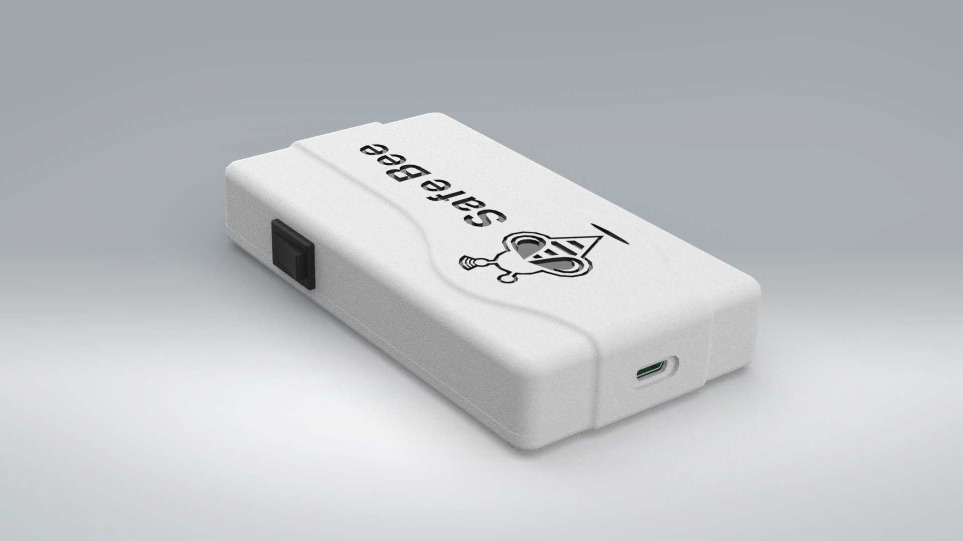
A 3D model of the enclosure is designed using Solidworks with overall dimensions of 60 x 20 x 112 mm. The enclosure has two holes, one for the charging micro USB connector and one to fit a mini rocker power switch. The provided design files (download .STEP and .STL files below) can be used to print your own enclosure in your desired color and material. The screws used to secure the enclosure are M3 x 10mm countersunk screws. Design is made by professional engineer janangachandima and you can find his services on the Fiverr page.
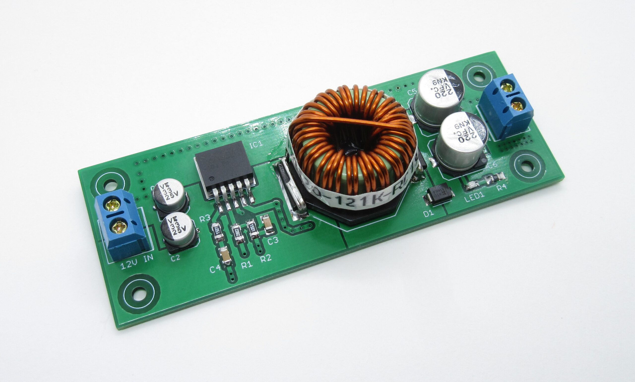
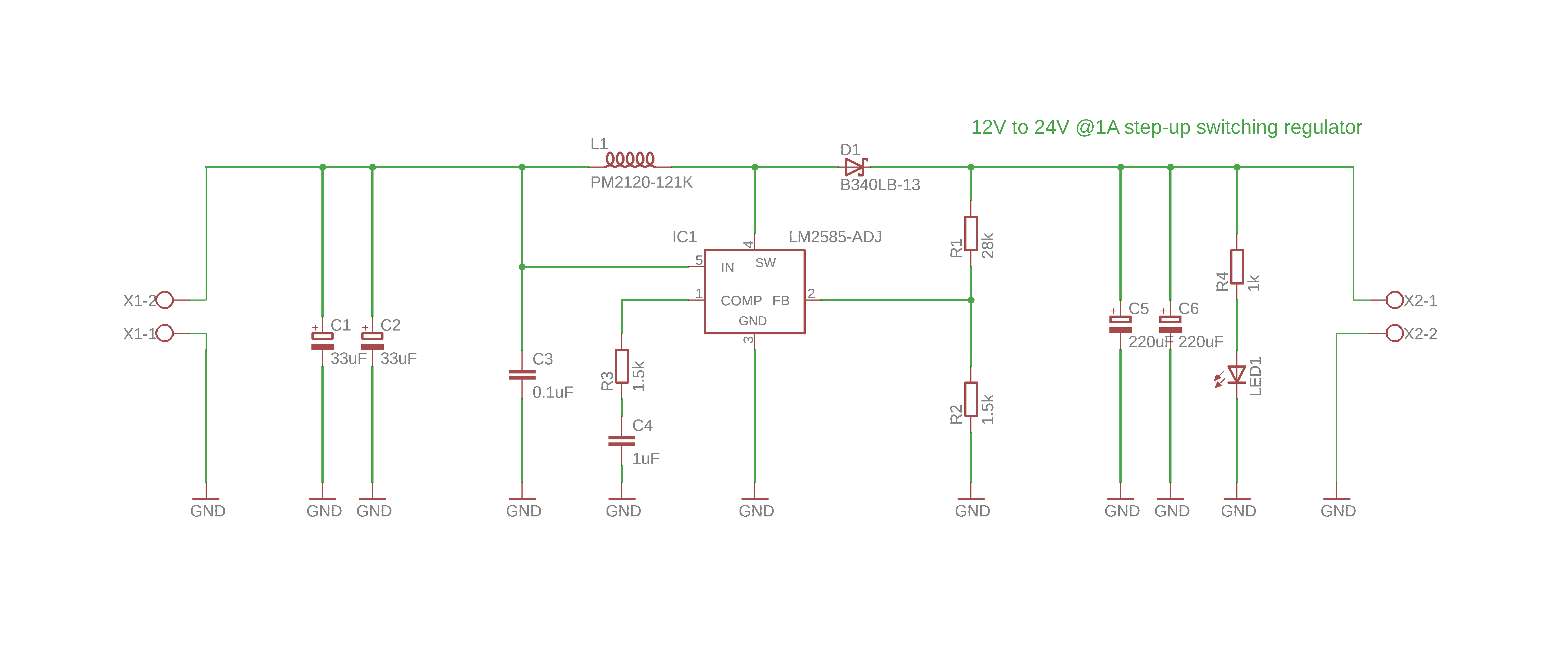
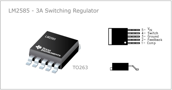
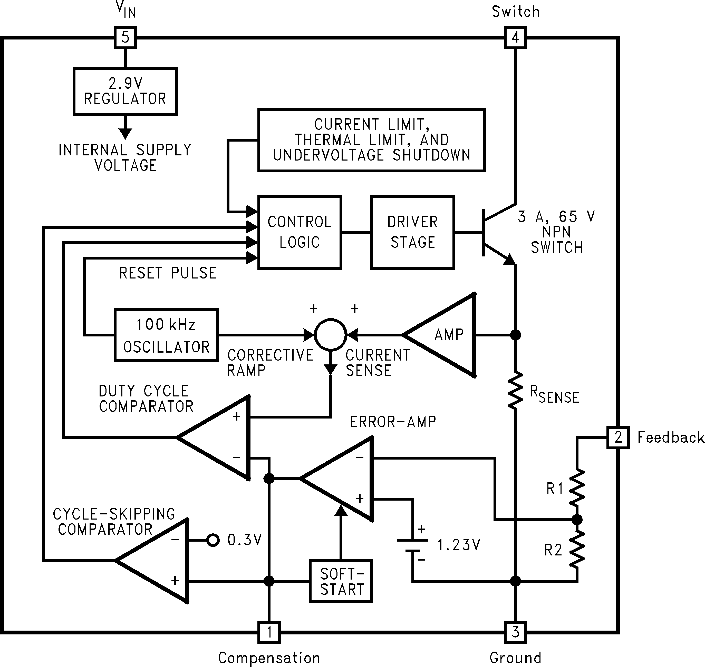
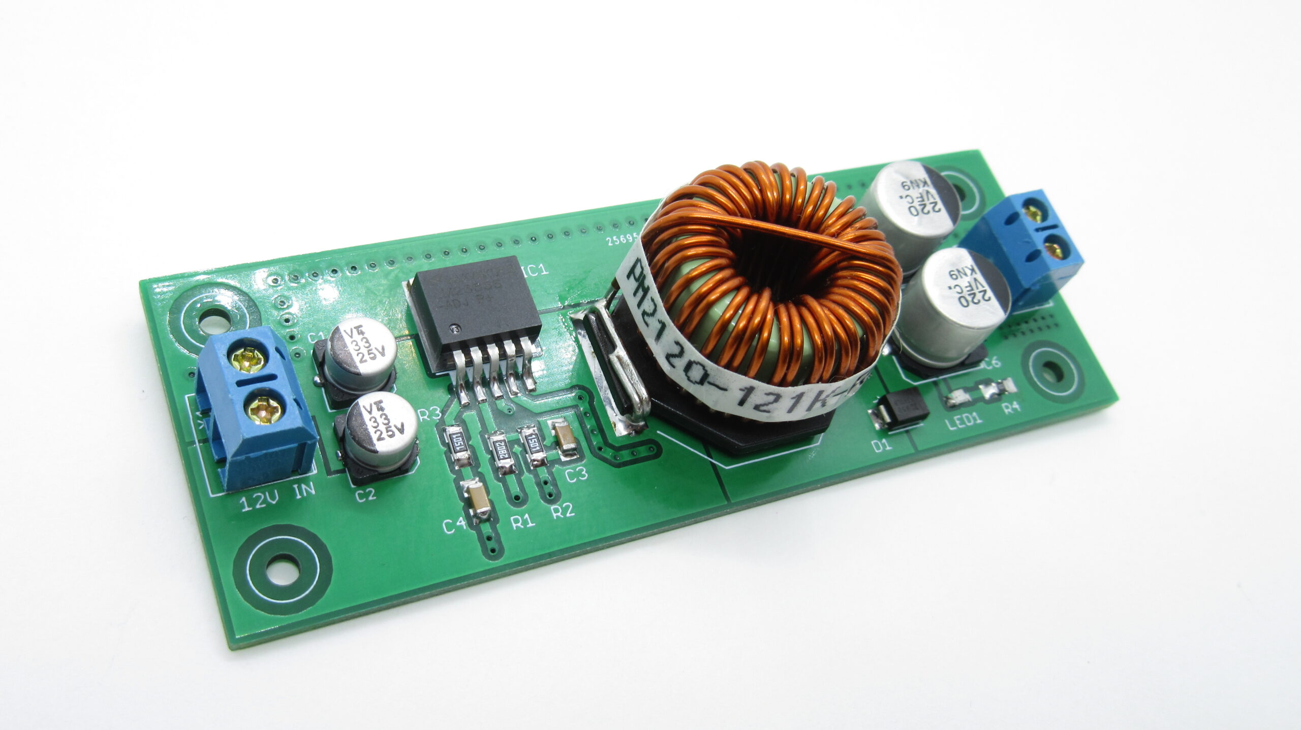
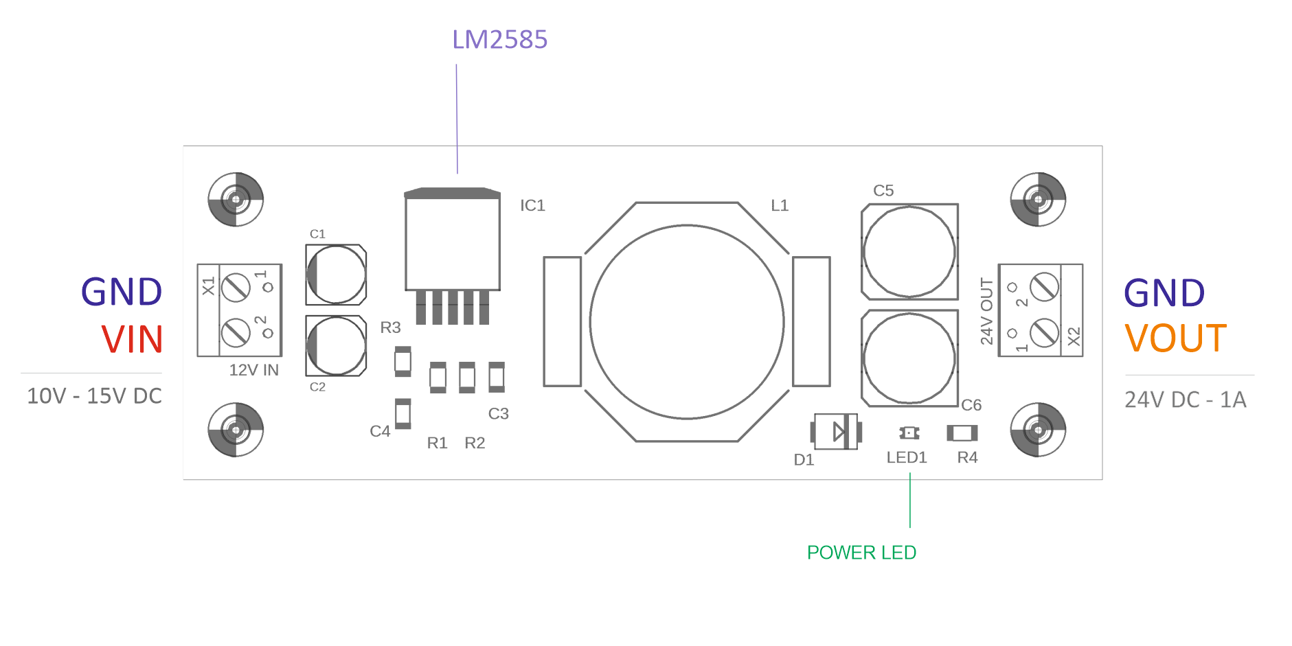
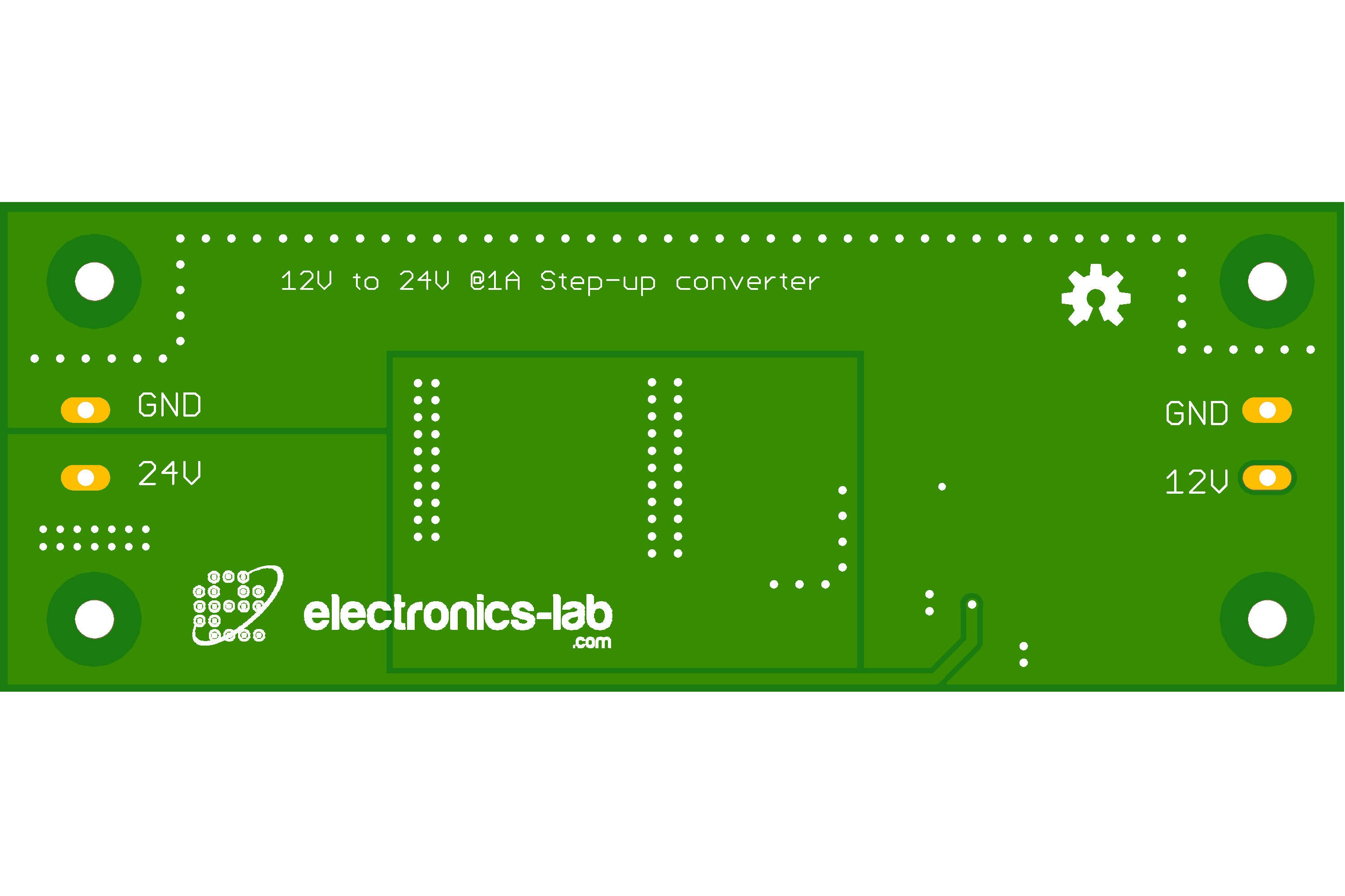
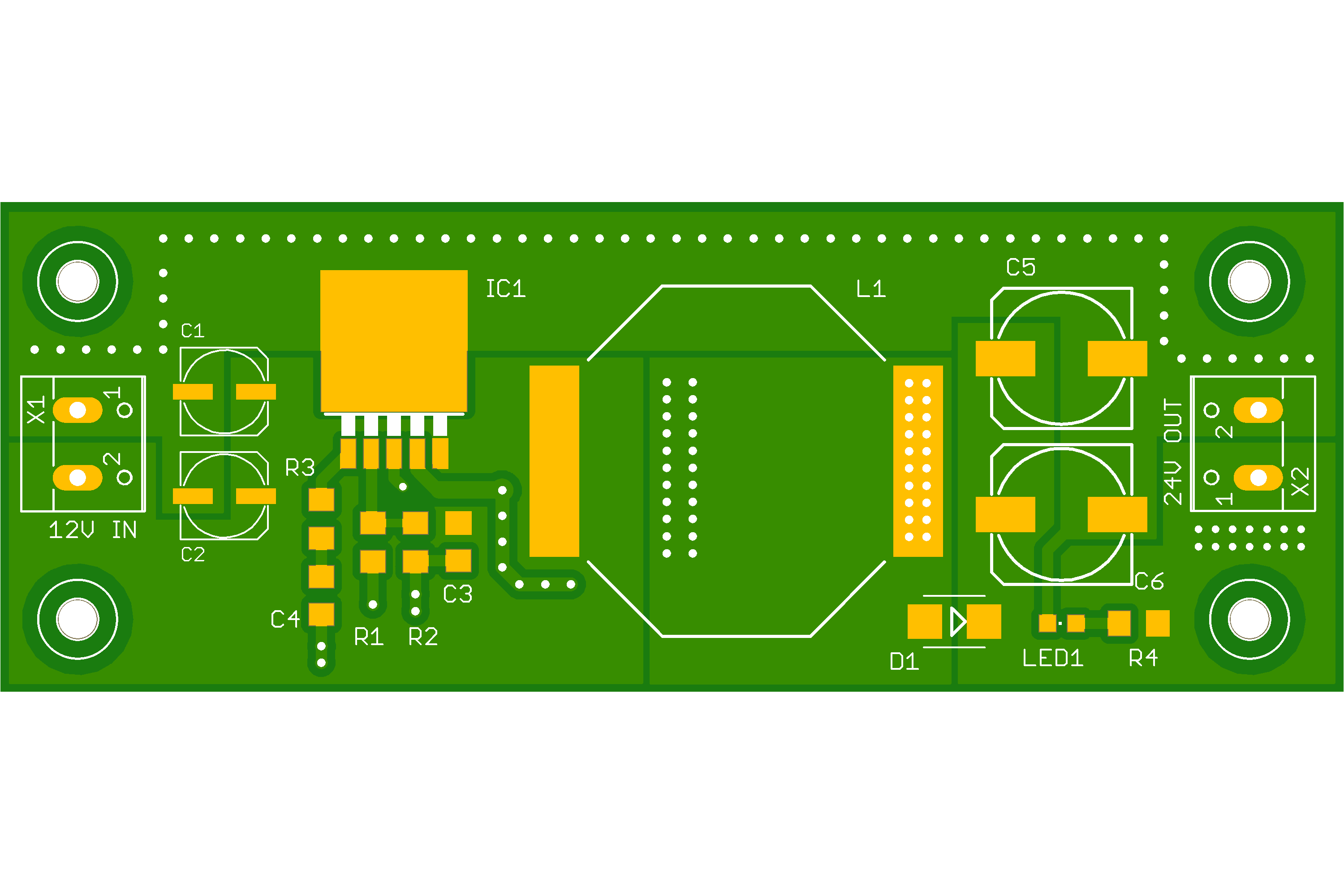
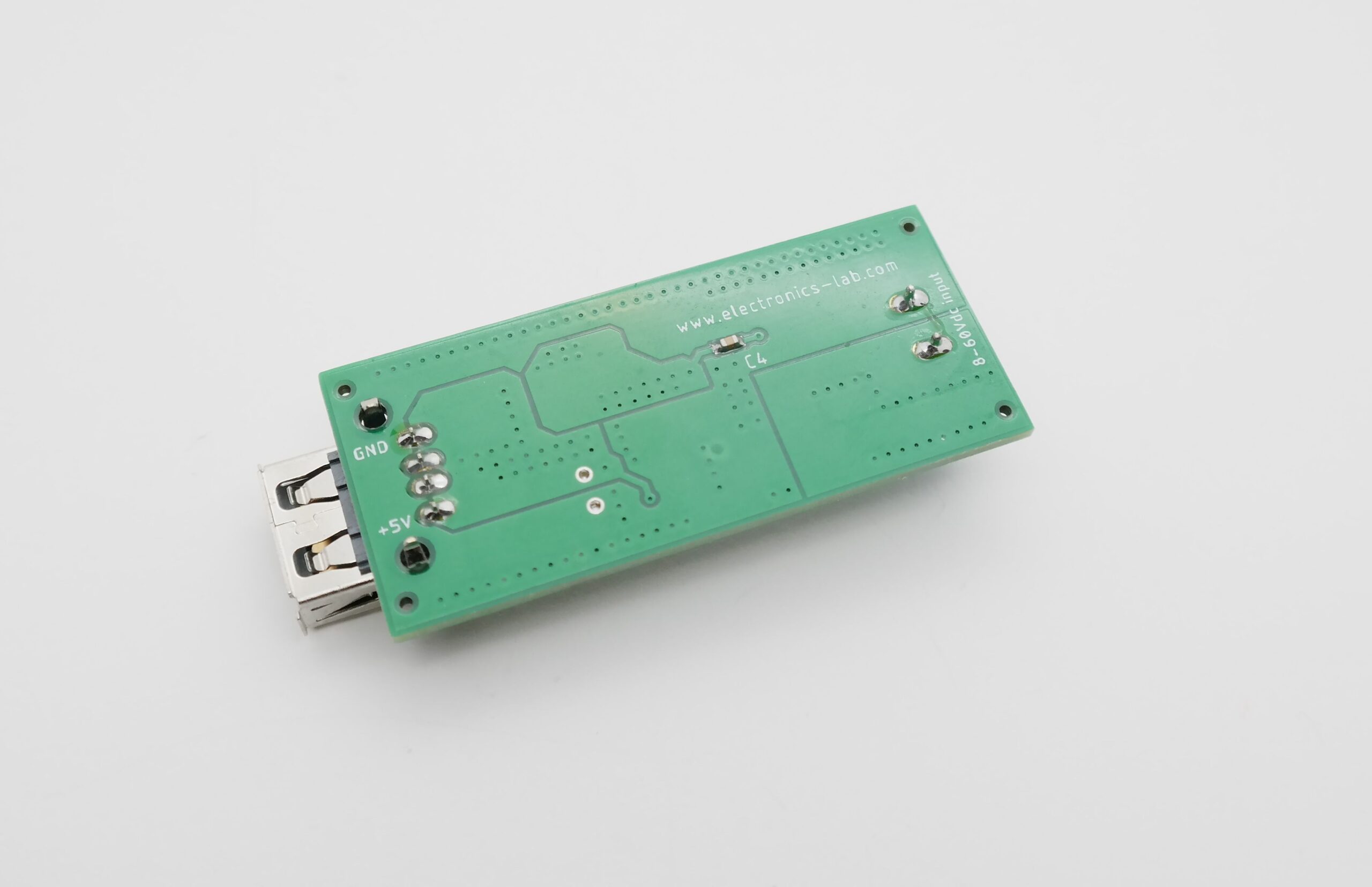
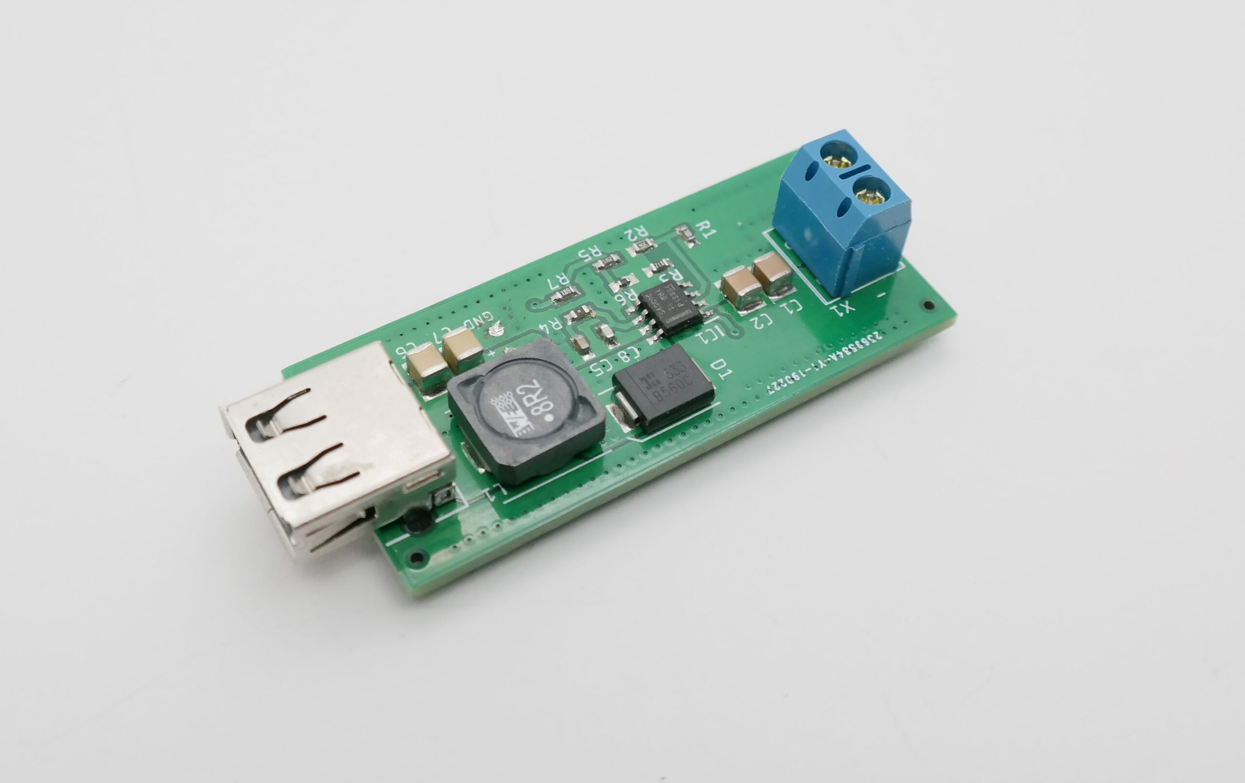
This is a DC-DC step-up converter based on LM2585-ADJ regulator manufactured by Texas Instruments. This IC was chosen for its simplicity of use, requiring minimal external components and for its ability to control the output voltage by defining the feedback resistors (R1,R2). NPN switching/power transistor is integrated inside the regulator and is able to withstand 3A maximum current and 65V maximum voltage. Switching frequency is defined by internal oscillator and it’s fixed at 100KHz.
The power switch is a 3-A NPN device that can standoff 65 V. Protecting the power switch are current and thermal limiting circuits and an under-voltage lockout circuit. This IC contains a 100-kHz fixed-frequency internal oscillator that permits the use of small magnetics. Other features include soft start mode to reduce in-rush current during start-up, current mode control for improved rejection of input voltage, and output load transients and cycle-by-cycle current limiting. An output voltage tolerance of ±4%, within specified input voltages and output load conditions, is specified for the power supply system.
Specifications
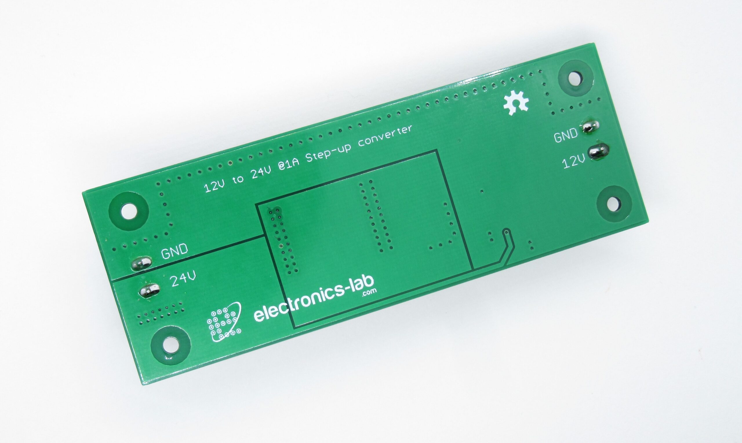
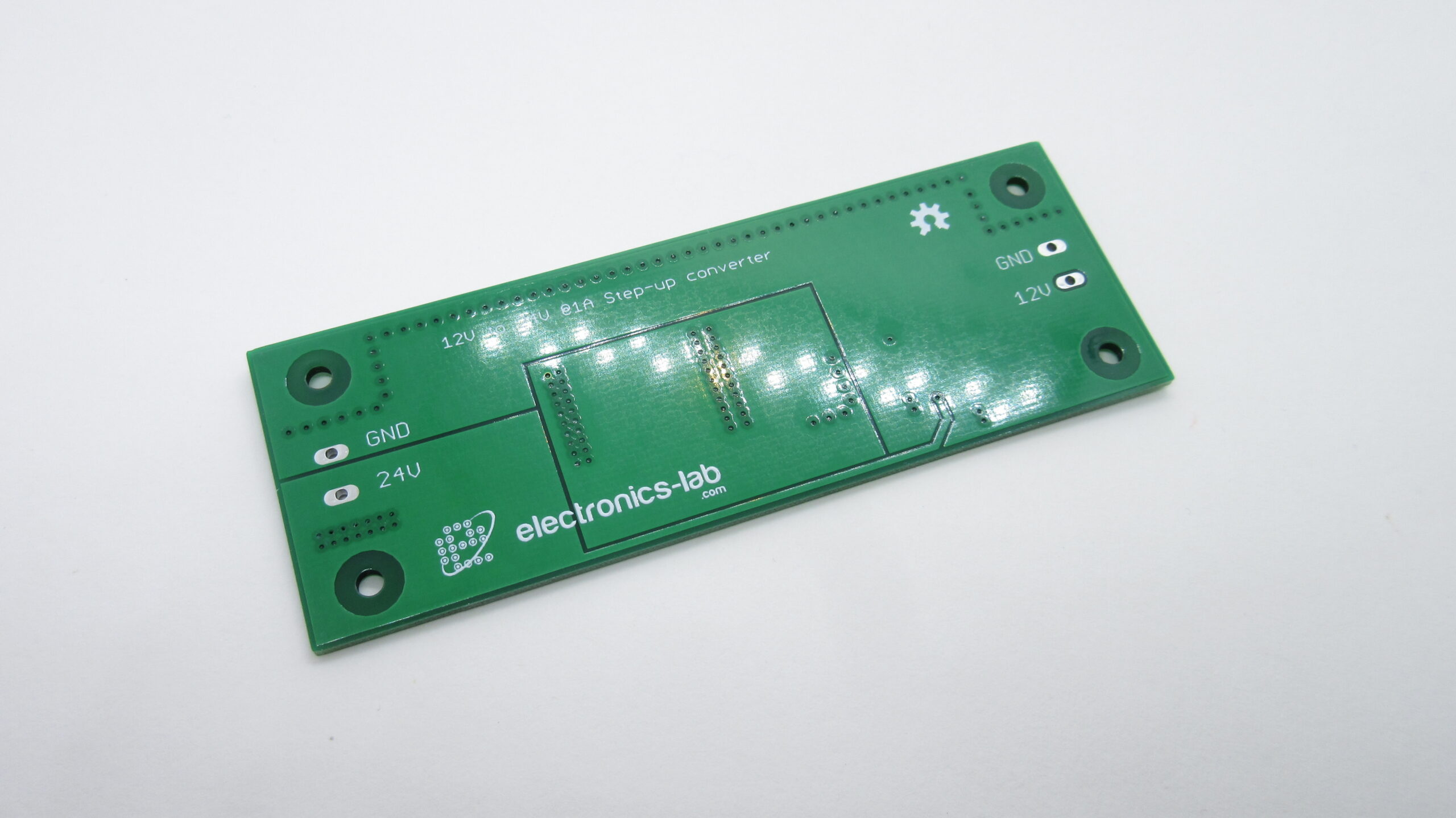
Vin: 10-15V DC
Vout: 24V DC
Iout: 1A (can go up to 1.5A with forced cooling)
Switching Frequency: 100KHz
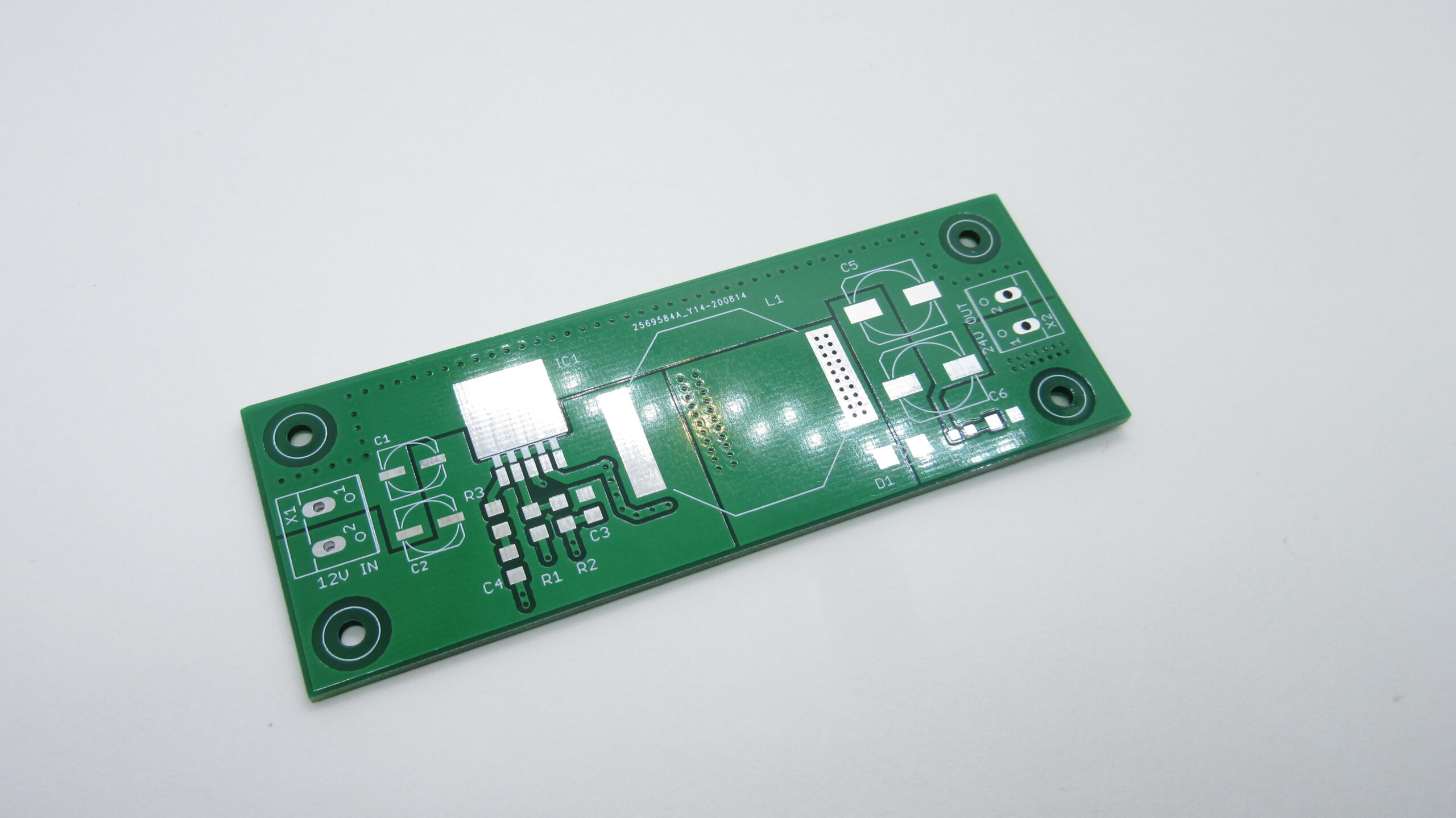
Schematic is a simple boost topology arrangement based on datasheet. Input capacitors and diode should be placed close enough to the regulator to minimize the inductance effects of PCB traces. IC1, L1, D1, C1,C2 and C5,C6 are the main parts used in voltage conversion. Capacitor C3 is a high-frequency bypass capacitor and should be placed as close to IC1 as possible.
All components are selected for their low loss characteristics. So capacitors selected have low ESR and inductor selected has low DC resistance.
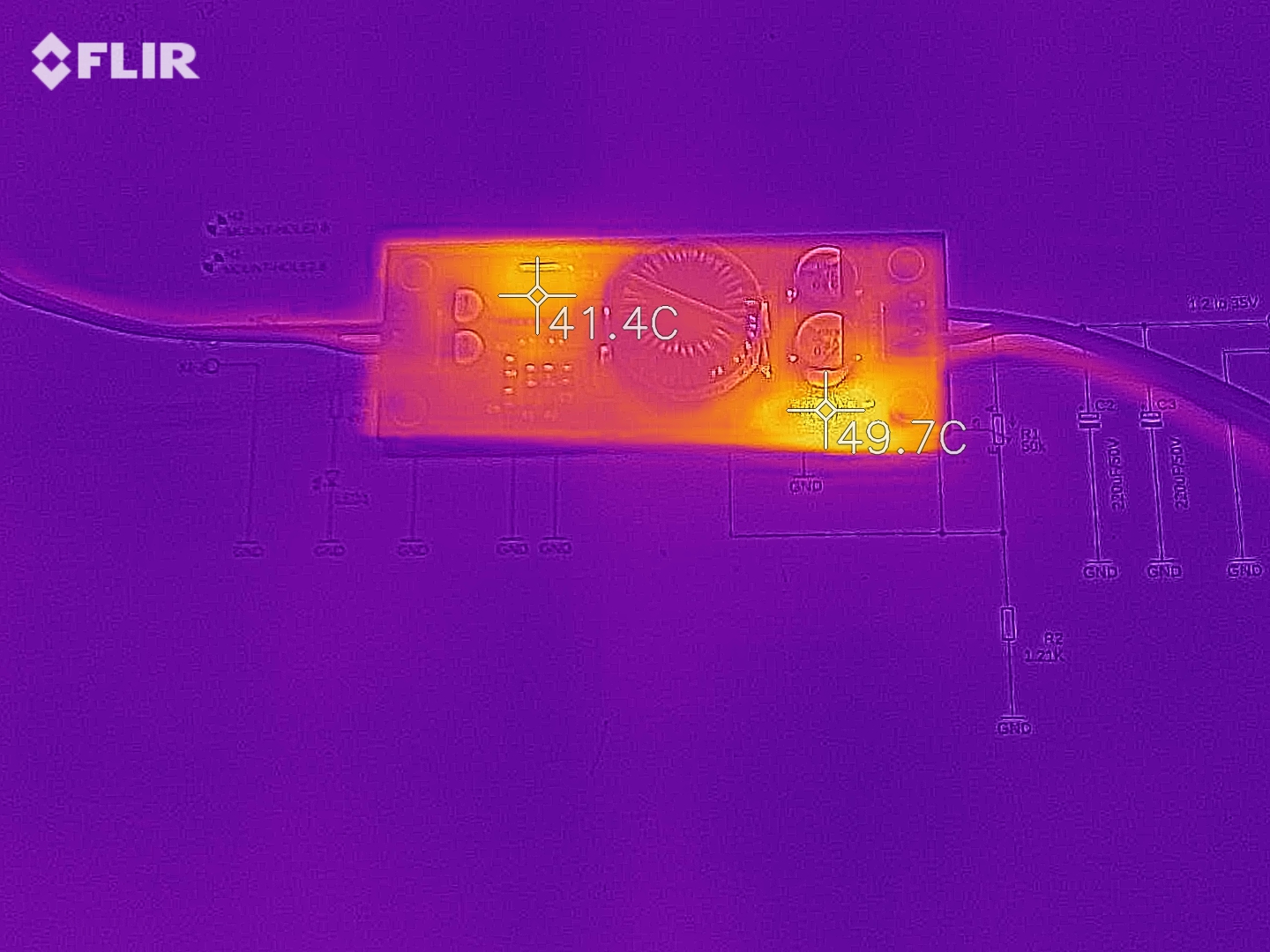
At maximum output power, there is significant heat produced by IC1 and for that reason, we mounted it directly on the ground plane to achieve maximum heat dissipation.
Block Diagram
Measurements
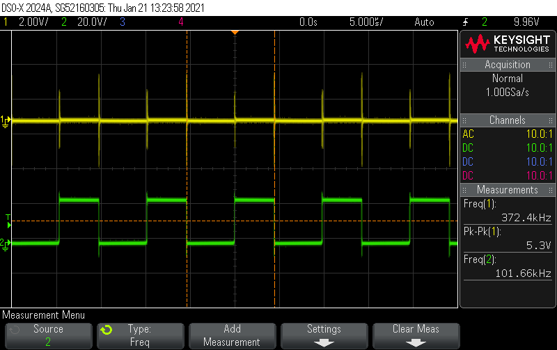
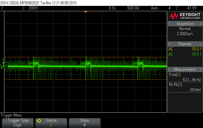
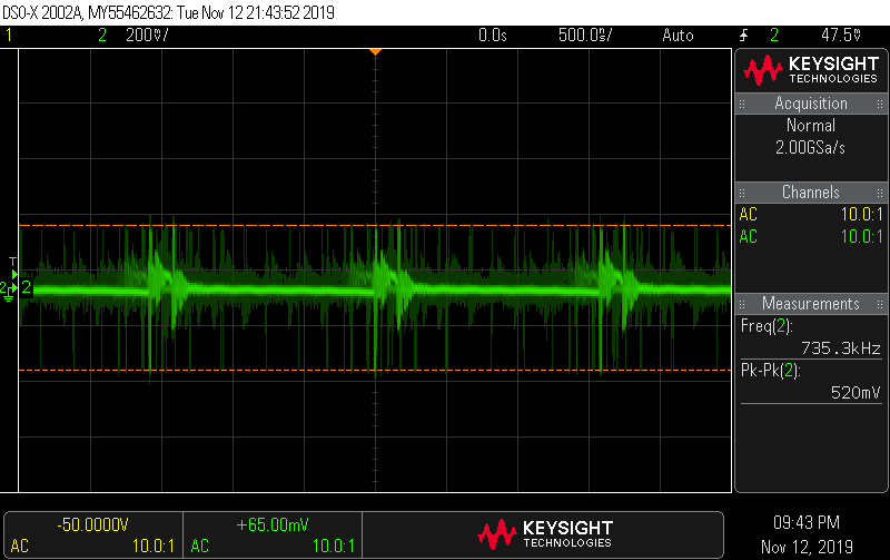
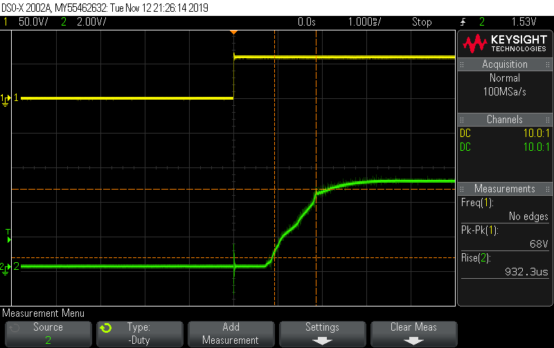
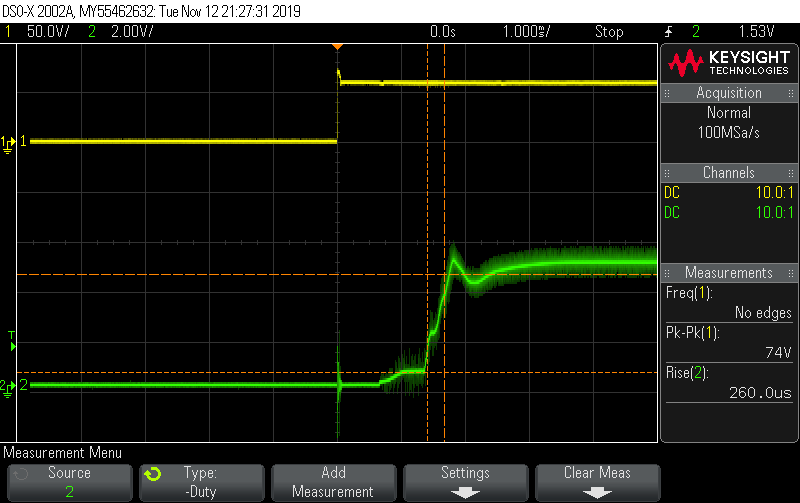
CH1: Output Voltage ripple with 12V Input and 24V @ 500mA output – 5.3 Vpp – CH2: voltage at PIN 4 of IC1CH1: Output Voltage ripple with 12V Input and 24V @ 1A output – 4.6Vpp – CH2: voltage at PIN 4 of IC1
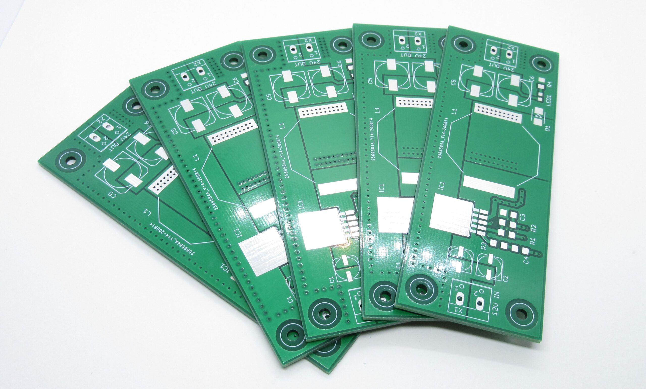
If you would like to receive a PCB, we can ship you one for 6$ (worldwide shipping) click here to contact us
Parts List
Part
Value
Package
MPN
Mouser No
C1 C2
33uF 25V 1Ω
6.3 x 5.4mm
UWX1E330MCL1GB
647-UWX1E330MCL1
C3
0.1uF 50V 0Ω
1206
C1206C104J5RACTU
80-C1206C104J5R
C4
1uF 25V
1206
C1206C105K3RACTU
80-C1206C105K3R
C5 C6
220uF 35V 0.15Ω
10 x 10.2mm
EEE-FC1V221P
667-EEE-FC1V221P
D1
0.45 V 3A 40V Schottky
SMB
B340LB-13-F
621-B340LB-F
IC1
LM2585S-ADJ
TO-263
LM2585S-ADJ/NOPB
926-LM2585S-ADJ/NOPB
L1
120 uH 0.04Ω
30.5 x 25.4 x 22.1 mm
PM2120-121K-RC
542-PM2120-121K-RC
R1
28 KΩ
1206
ERJ-8ENF2802V
667-ERJ-8ENF2802V
R2 R3
1.5 KΩ
1206
ERJ-8ENF1501V
667-ERJ-8ENF1501V
R4
1 KΩ
1206
RT1206FRE07931KL
603-RT1206FRE07931KL
LED1
RED LED 20mA 2.1V
0805
599-0120-007F
645-599-0120-007F
Connections
Gerber View
Simulation
We’ve done a simulation of the LM2585 step-up DC-DC converter using the TI’s WEBENCH online software tools and some of the results are presented here.
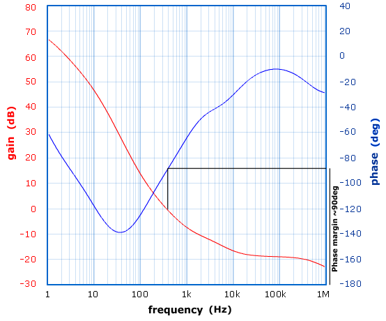
The first graph is the open-loop BODE graph. In this graph, we see a plot of GAIN vs FREQUENCY in the range 1Hz – 1M and PHASE vs FREQUENCY in the same range. This plot is useful as it gives us a detailed view of the stability of the loop and thus the stability and performance of our DC-DC converter.
Bode plot of open control loop
What’s interesting on this plot is the “phase margin” and “gain margin“. The gain margin is the gain for -180deg phase shift and phase margin is the phase difference from 180deg for 0db gain as shown in the plot above. For the system to be considered stable there should be enough phase margin (>30deg) for 0db gain or when phase is -180deg the gain should be less than 0db.
On the plot above we see that the phase margin is ~90deg and that ensures that the DC-DC converter will be stable over the measured range.
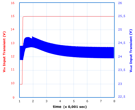
The next simulation graph is the Input Transient plot over time.
Input Transient simulation
In this plot, we see how the output voltage is recovering when the input voltage is stepped from 10V to 15V. We see that 4ms after the input voltage is stepped the output has recovered to the normal output voltage of 24V.
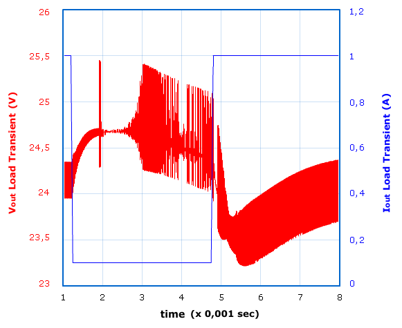
The next graph is the Load Transient.
Load Transient simulation
Load transient is the response of output voltage to sudden changes of load or Iout. We see that the output current suddenly changes from 0,1A to 1A and that the output voltage drops down to 23,2V until it recovers in about 3ms. We also see that when the load is reduced from 1A to 0,1A, output voltage spikes up to ~25,5V, then rings until it recovers to 24V in about 4ms.
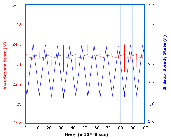
The last graph shows the Steady State operation of DC-DC converter @ 1A output.
This graph shows the simulated output voltage ripple and inductor current. We see that output voltage ripple is ~0,6Vpp and the inductor current has a peak current of 2,4A. The inductor we used is rated at max 5,6A DC so it can easily withstand such operating current and without much heating of the coil.
Operating point data (Vin=13V, Iout=1A)
Operating Values
Pulse Width Modulation (PWM) frequency
Frequency
100 kHz
Continuous or Discontinuous Conduction mode
Mode
Cont
Total Output Power
Pout
24.0 W
Vin operating point
Vin Op
13.00 V
Iout operating point
Iout Op
1.00 A
Operating Point at Vin= 13.00 V,1.00 A
Bode Plot Crossover Frequency, indication of bandwidth of supply
Cross Freq
819 Hz
Steady State PWM Duty Cycle, range limits from 0 to 100
Duty Cycle
48.3 %
Steady State Efficiency
Efficiency
93.2 %
IC Junction Temperature
IC Tj
65.2 °C
IC Junction to Ambient Thermal Resistance
IC ThetaJA
34.9 °C/W
Current Analysis
Input Capacitor RMS ripple current
Cin IRMS
0.14 A
Output Capacitor RMS ripple current
Cout IRMS
0.48 A
Peak Current in IC for Steady State Operating Point
IC Ipk
2.2 A
ICs Maximum rated peak current
IC Ipk Max
3.0 A
Average input current
Iin Avg
2.0 A
Inductor ripple current, peak-to-peak value
L Ipp
0.50 A
Power Dissipation Analysis
Input Capacitor Power Dissipation
Cin Pd
0.01 W
Output Capacitor Power Dissipation
Cout Pd
0.035 W
Diode Power Dissipation
Diode Pd
0.45 W
IC Power Dissipation
IC Pd
1.0 W
Inductor Power Dissipation
L Pd
0.16 W
Configuring Output Voltage
The output voltage is configured by R1, R2 according to the following expression (Vref=1,23V)
VOUT = VREF (1 + R1/R2)
If R2 has a value between 1k and 5k we can use this expression to calculate R1:
R1 = R2 (VOUT/VREF − 1)
For better thermal response and stability it is suggested to use 1% metal film resistors.
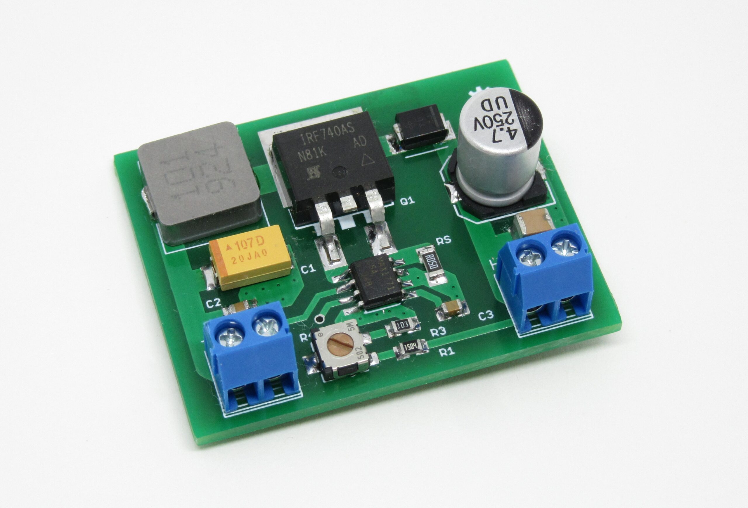
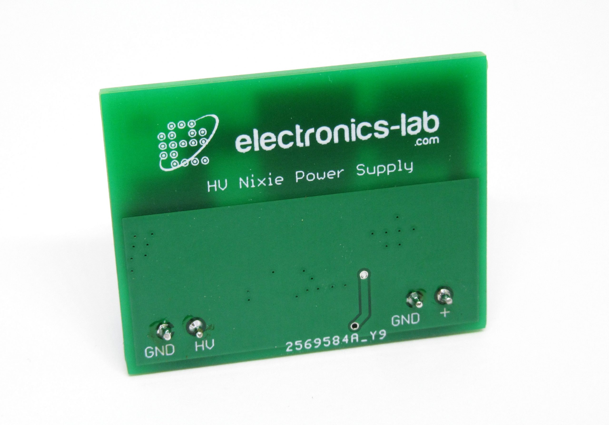
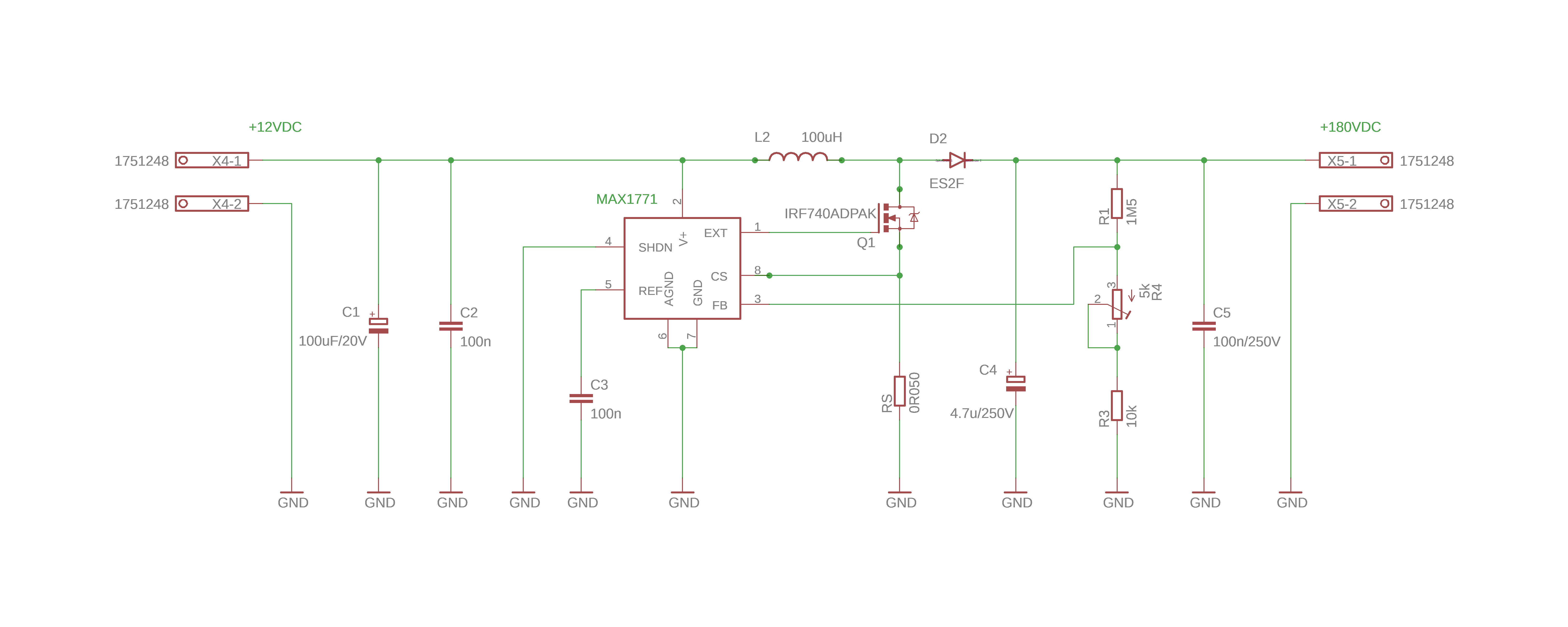
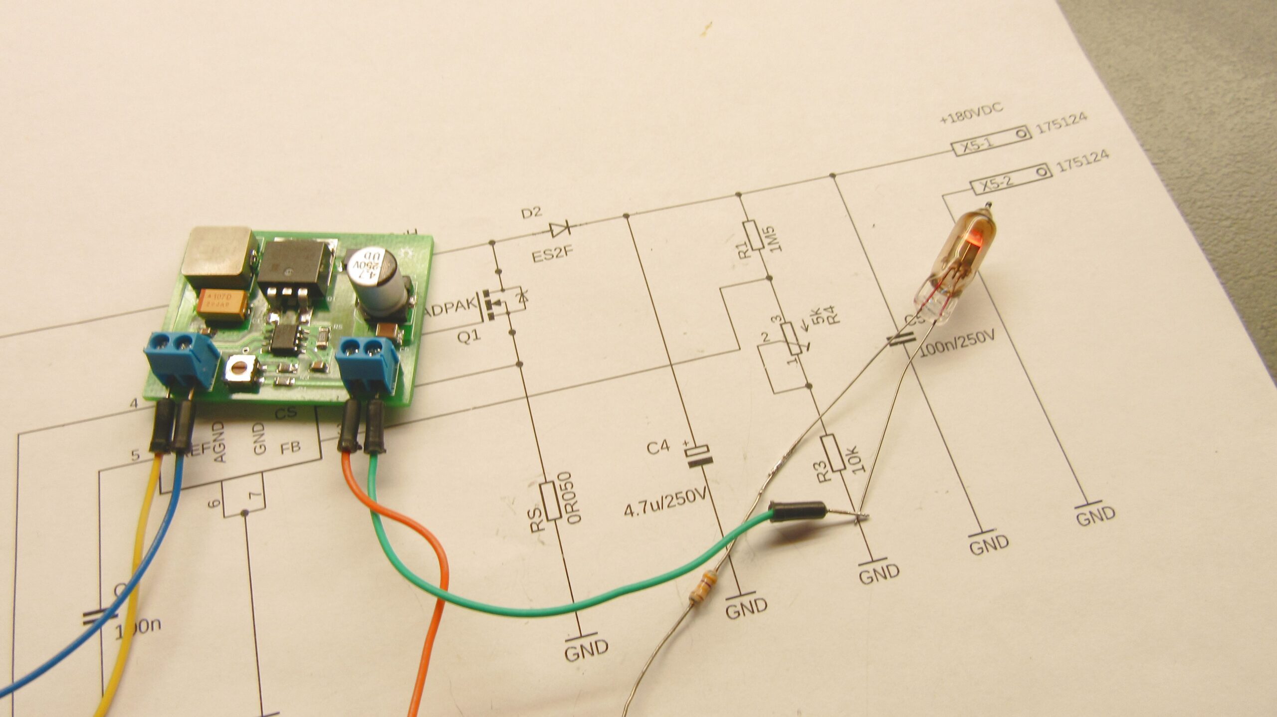
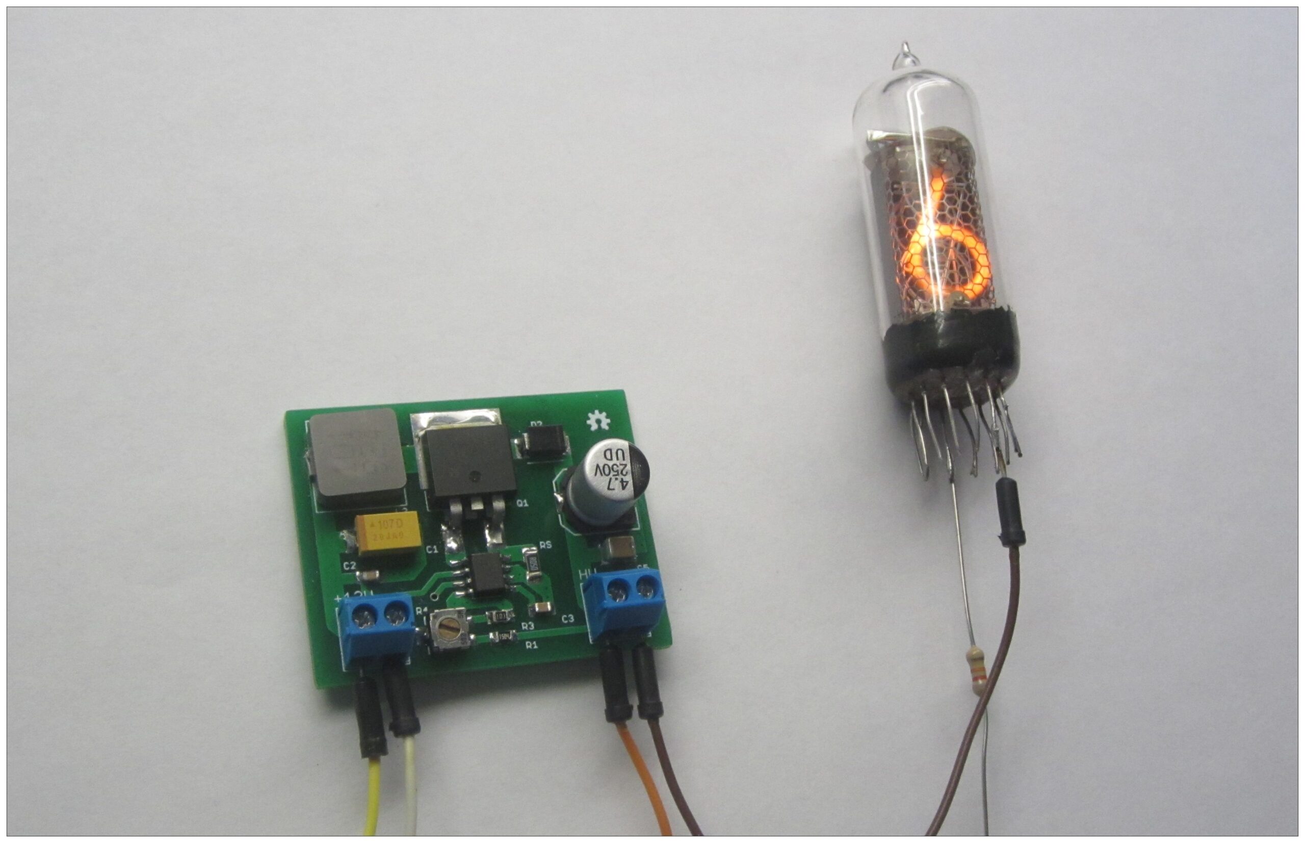
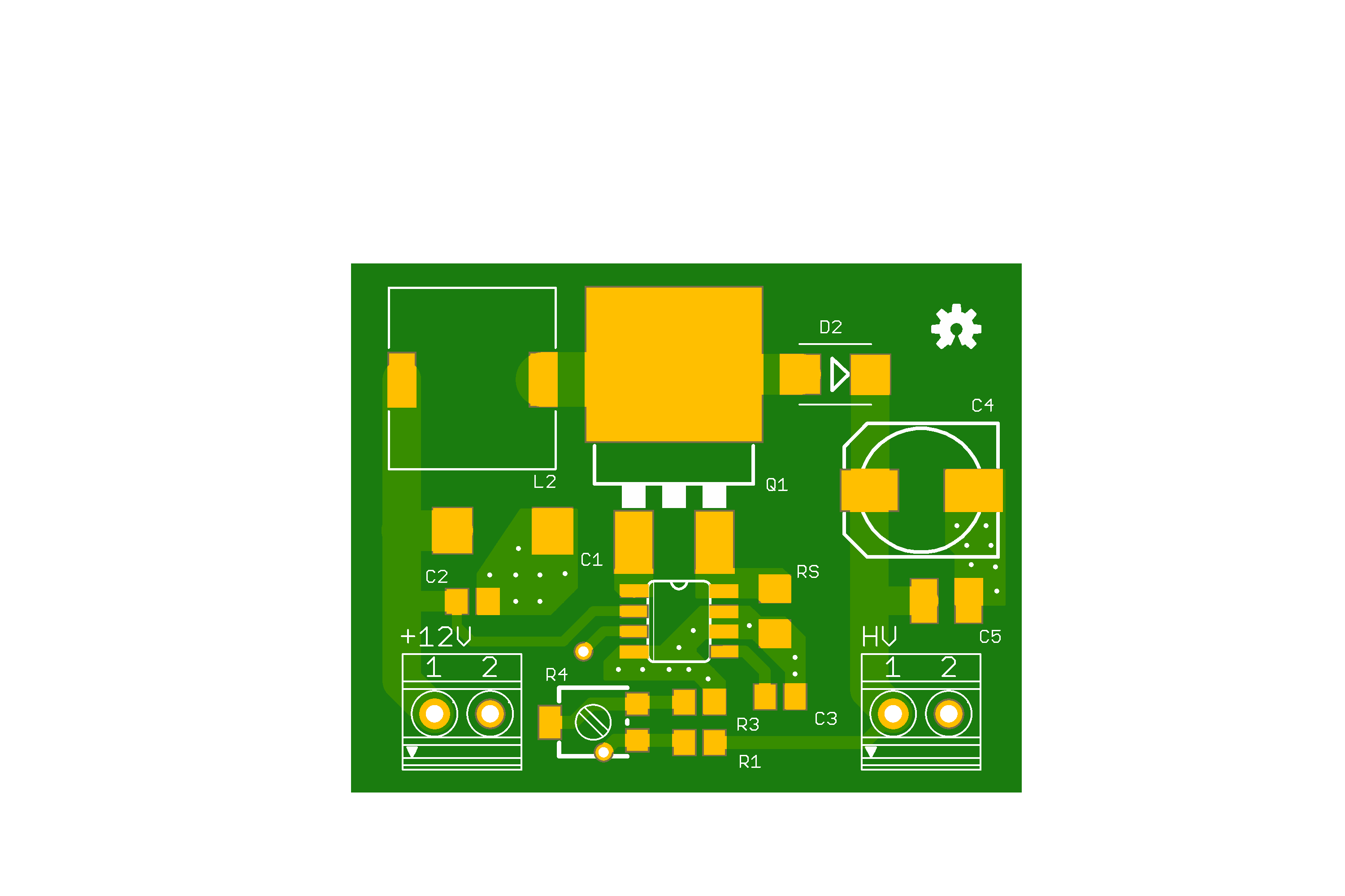
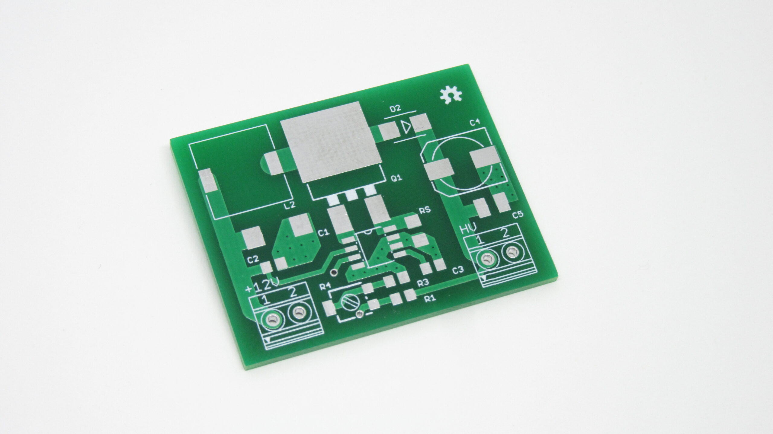
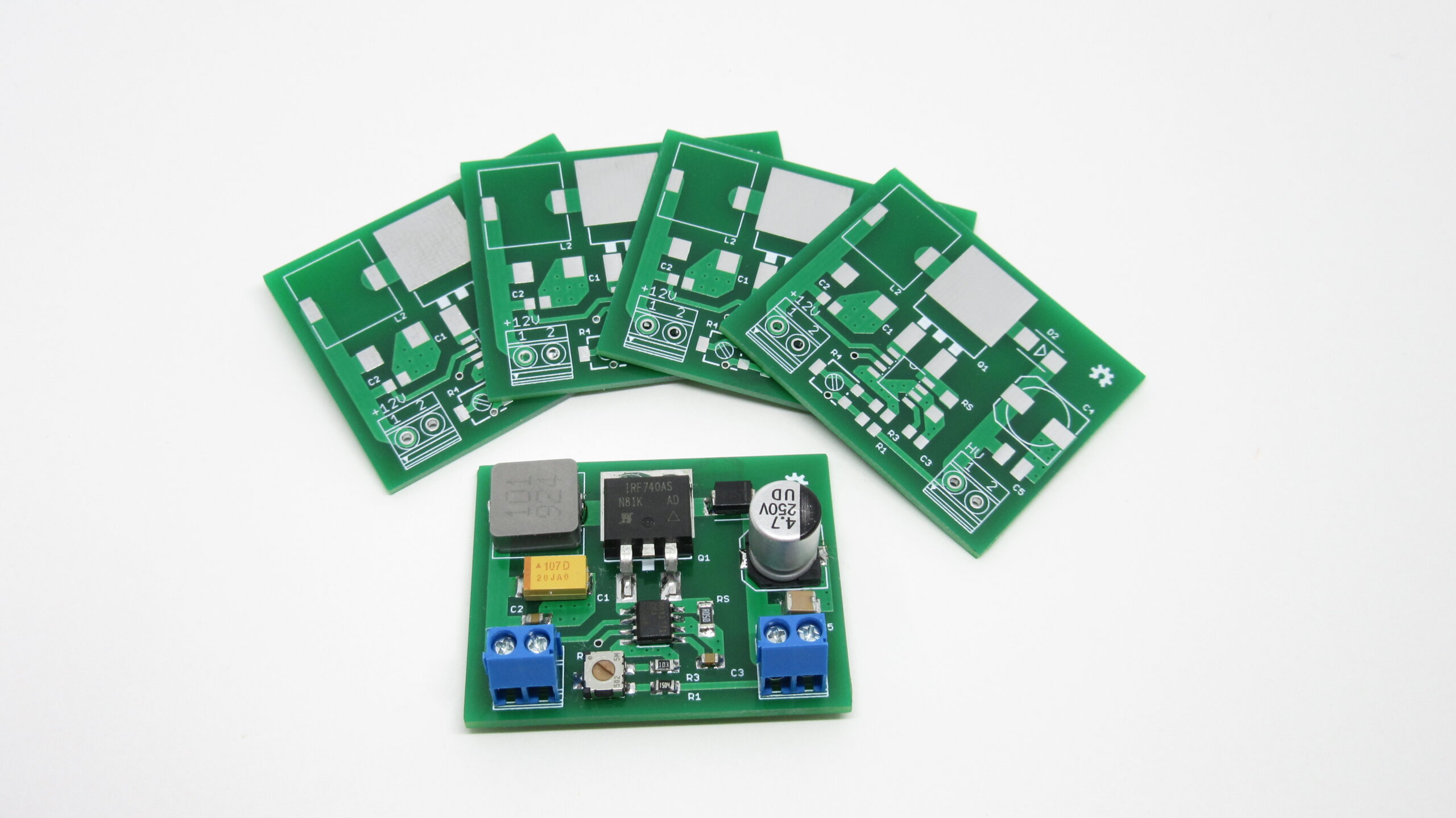
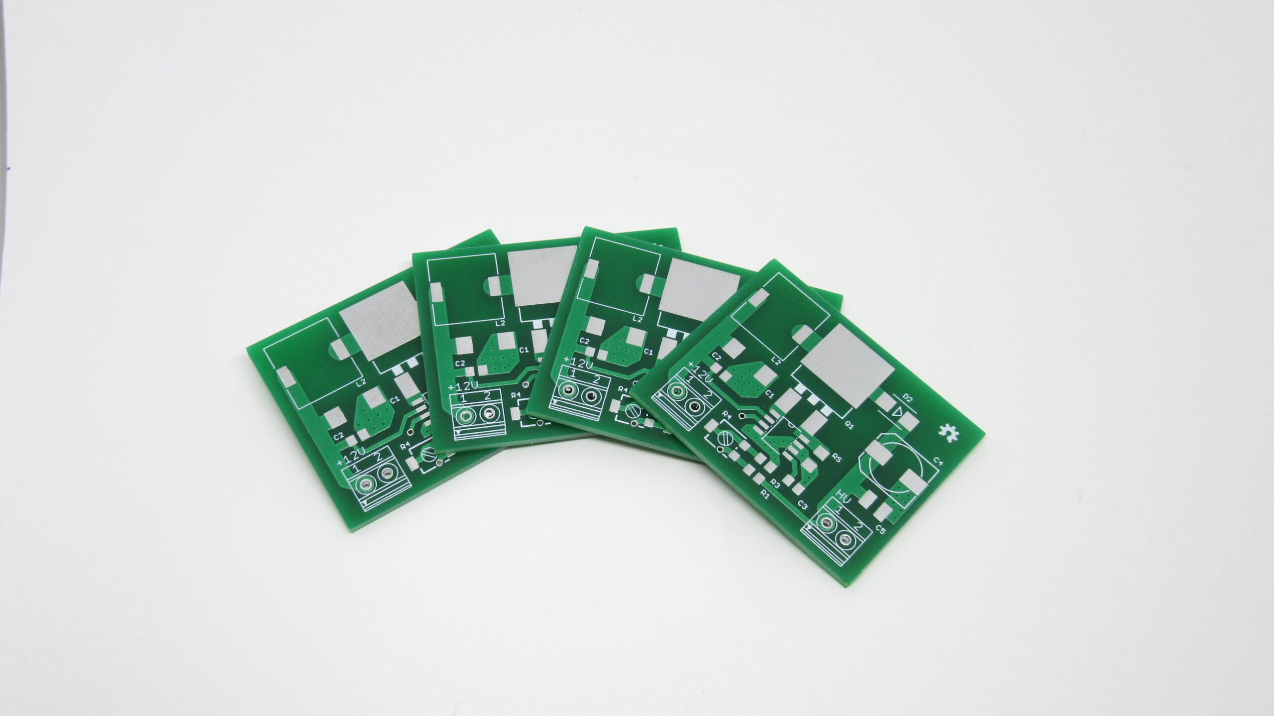
Nixie tubes need about ~180Vdc to light up and thus on most devices, a DC-DC converter is needed. Here we designed a simple DC-DC switching regulator capable of powering most of Nixie tubes. The board accepts 12Vdc input and gives an output of 150-250Vdc. The board is heavily inspired by Nick de Smith’s design.
Description
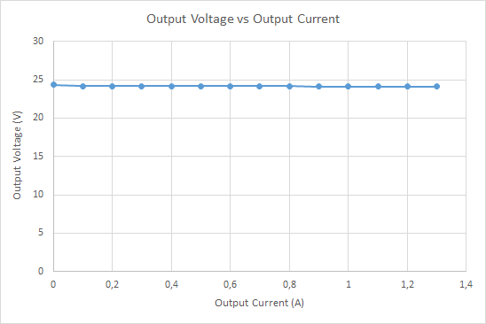
The module is based on the MAX1771 Step-Up DC-DC Controller. The controller works up to 300kHz switching frequency and that allows the usage of miniature surface mount components. In the default configuration, it accepts an input voltage from 2V to Vout and outputs 12V, but in this module, the output voltage is selected using the onboard potentiometer and it’s in the range 150-250Vdc. The maximum output current is 50mA @ 180Vdc.
The MAX1771 is driving an external N-channel MOSFET (IRF740) and with the help of the inductor and a fast diode, high voltage is produced.
MOSFET has to be low RDSon, the diode has to be fast Mttr, typically < 50nS, and capacitors have to be low ESR type to have good efficiency.
Precautions must be taken as this power supply uses high voltages. Build it only if you know what you are dealing with. Don’t touch any of the parts while in use.
Pay attention on the placement of C1 tantalum capacitor, as the bar indicates the anode (positive lead)
Schematic
Parts List
Part
Value
LCSC.com
R1
1.5M - 0805 SMD
C118025
R3
10k 0805
C269724
R4
5k trimmer SMD
C128557
Rs
0.05 Ohm - 0805 SMD
C149662
C1
100uF Tantalium SMD
C122302
C2, C3
100nF - 0805 SMD
C396718
C4
4.7uF / 250V SMD
C88702
C5
100nF / 250V SMD 1210
C52020
IC
MAX1771 SO-8
C407903
L1
100uH / 2.5 A
C2962892
Q1
IRF740 D2PAK (TO-263-2)
C39238
D2
ES2F-E3, ES2GB
C145321, C2844160
X1, X2
Screw Terminal - P=3.5mm
C474892
Oscilloscope Measurements
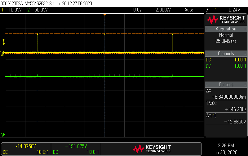
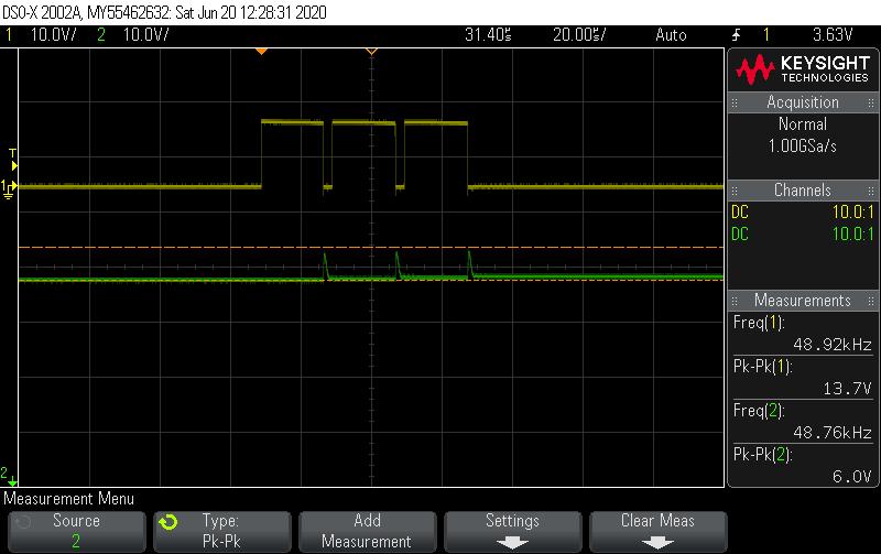
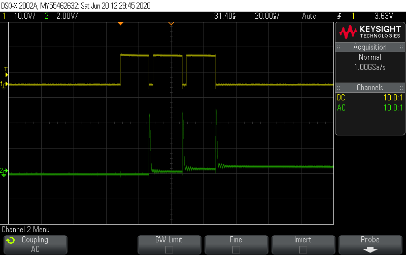
Yellow is the MOSFET Gate voltage and Green the output high voltage (~180Vdc). We see that the transistor switches with a low frequency of 146Hz and with a peak gate voltage of 12.8Vzoom in to the above short pulses reveals 3x pulses with 48.7Khz frequency to the gate of MOSFET. Also, the peak to peak ripple on output is 6Vfurther zoom to the output ripple reveals some short ringing and the peak ripple voltage.
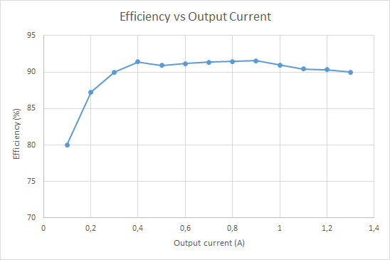
Efficiency
The module’s efficiency is calculated for two output currents (50mA and 25mA) at 180Vdc voltage output and 12V input. In the first case, the Pout = 8.1W while the Pin=10.96W, so efficiency is calculated at 73.9%. In the second case, the Pout = 4.1W while the Pin=5.52W, so efficiency is calculated at 74.2%. We see that for lower currents efficiency is a little greater than for the maximum current of 50mA.
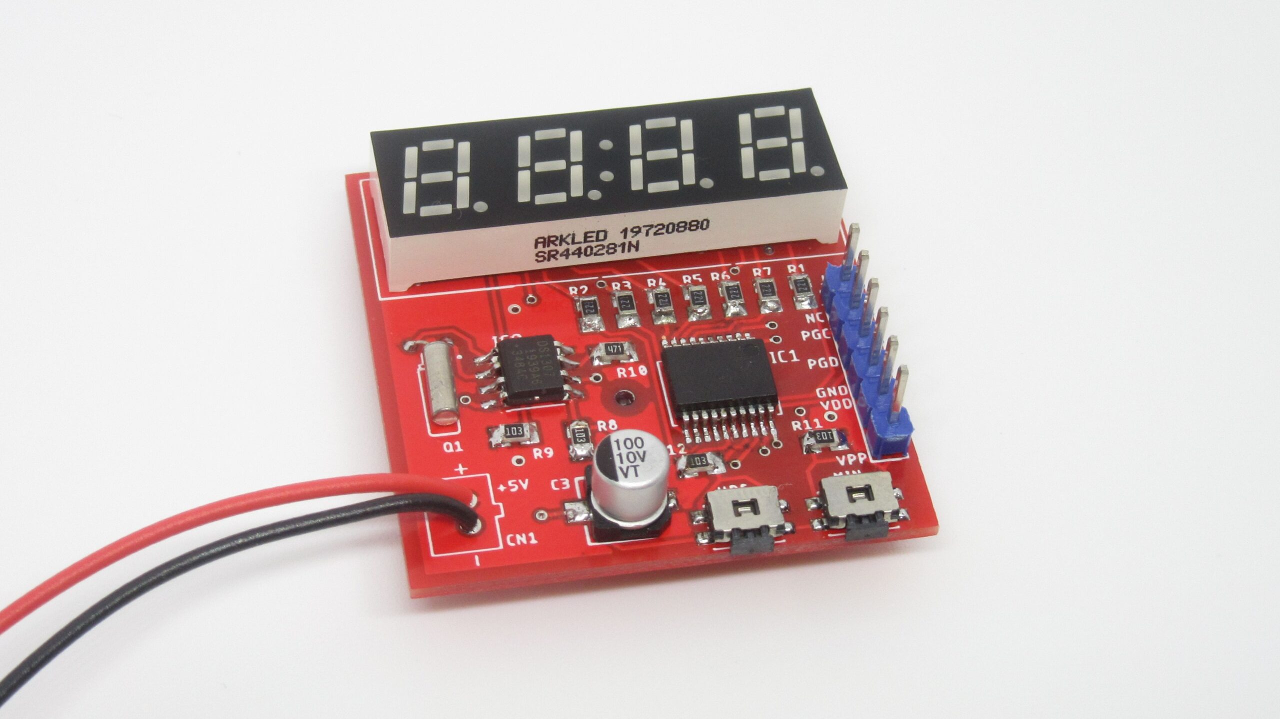
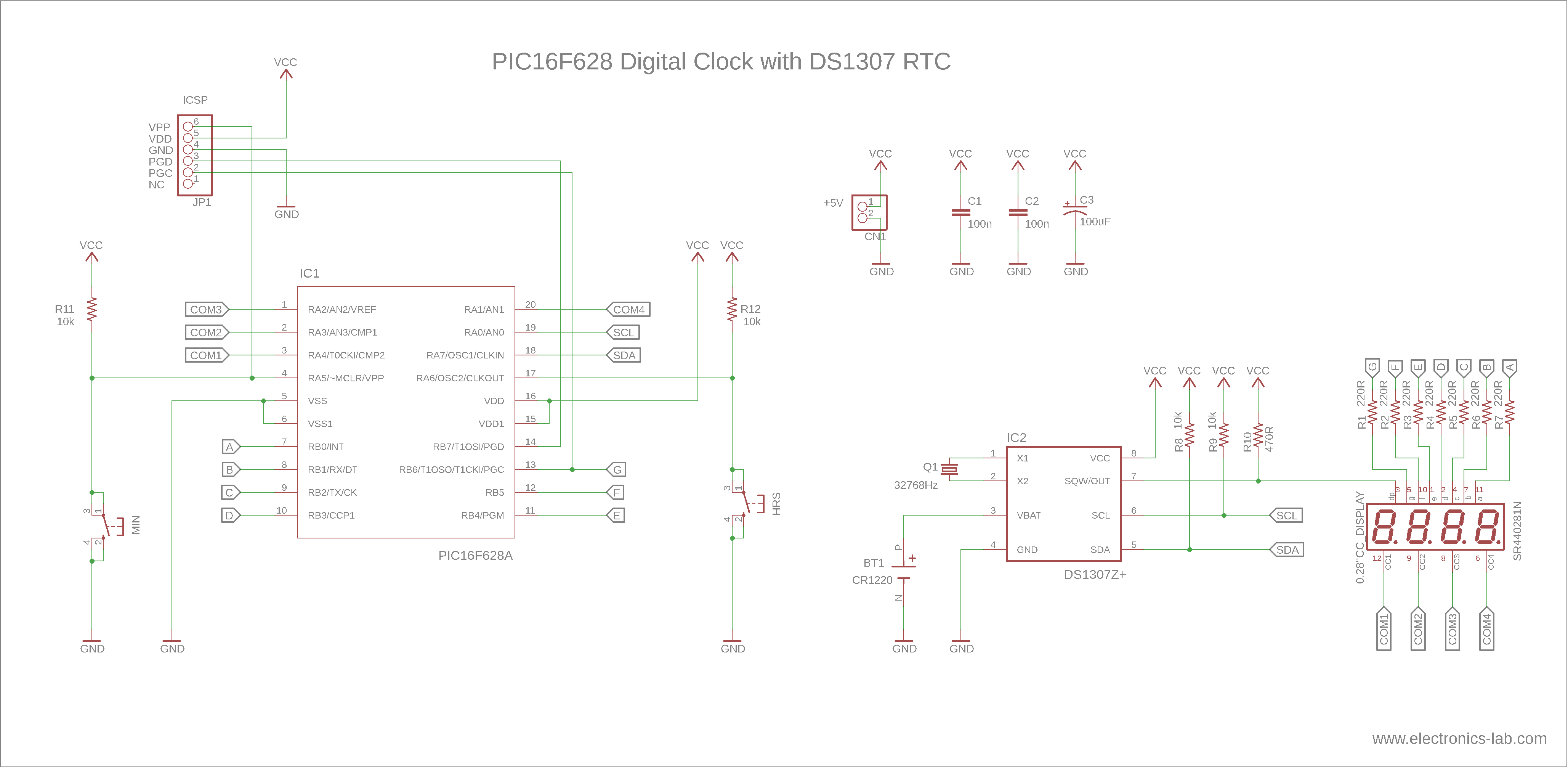
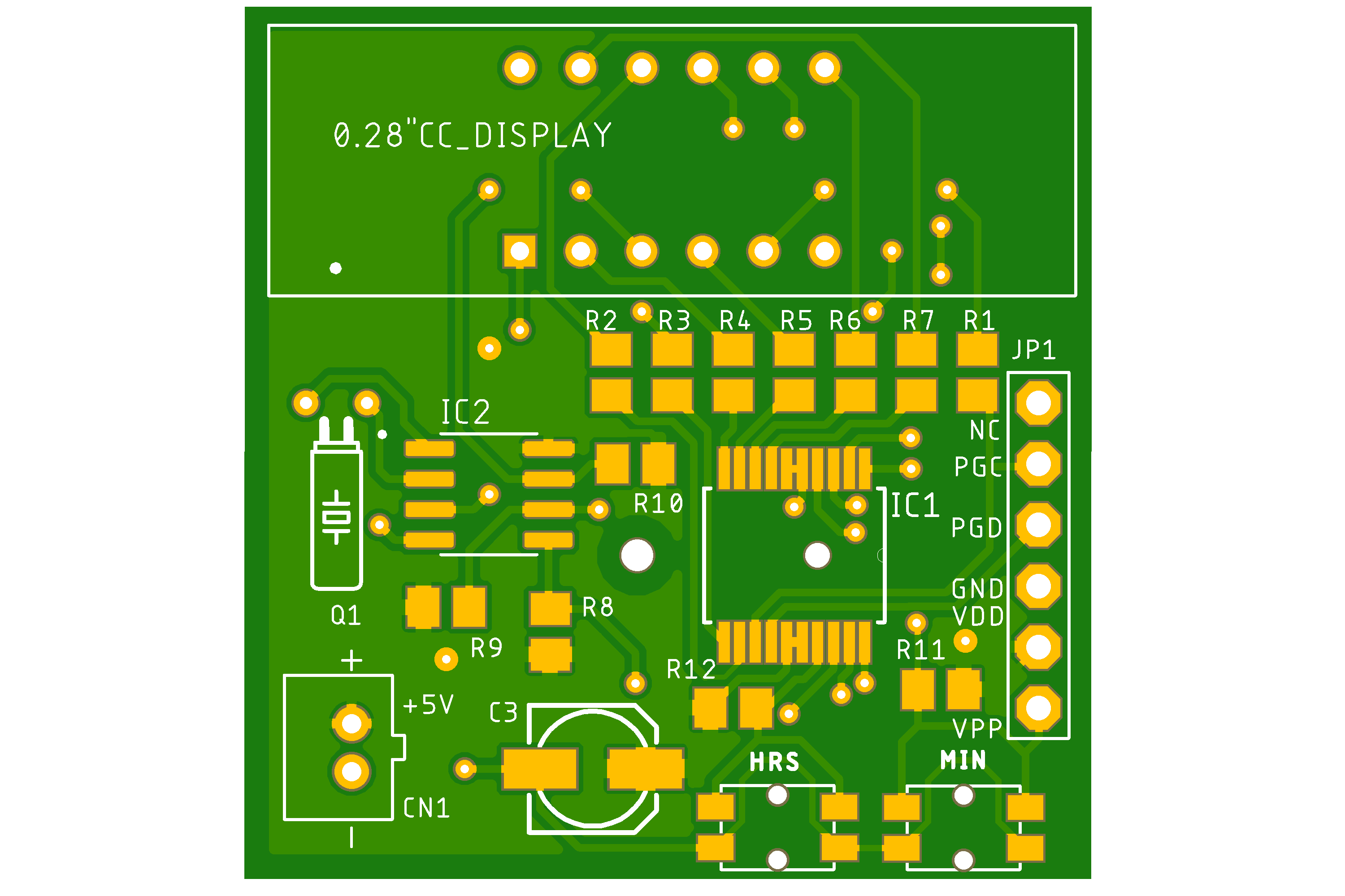
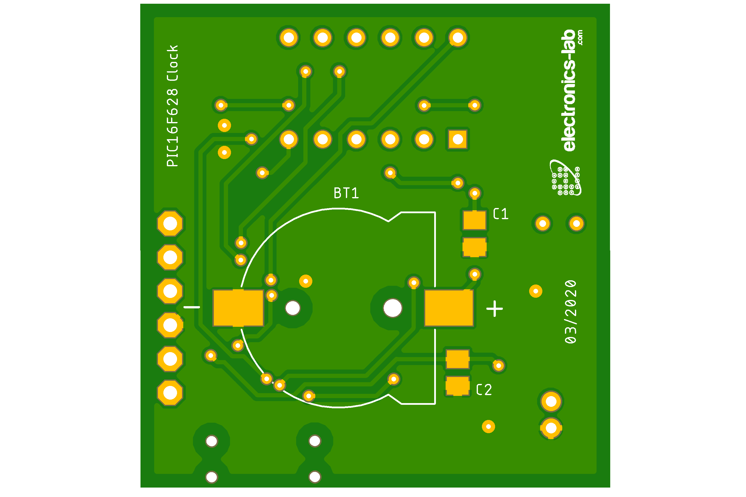
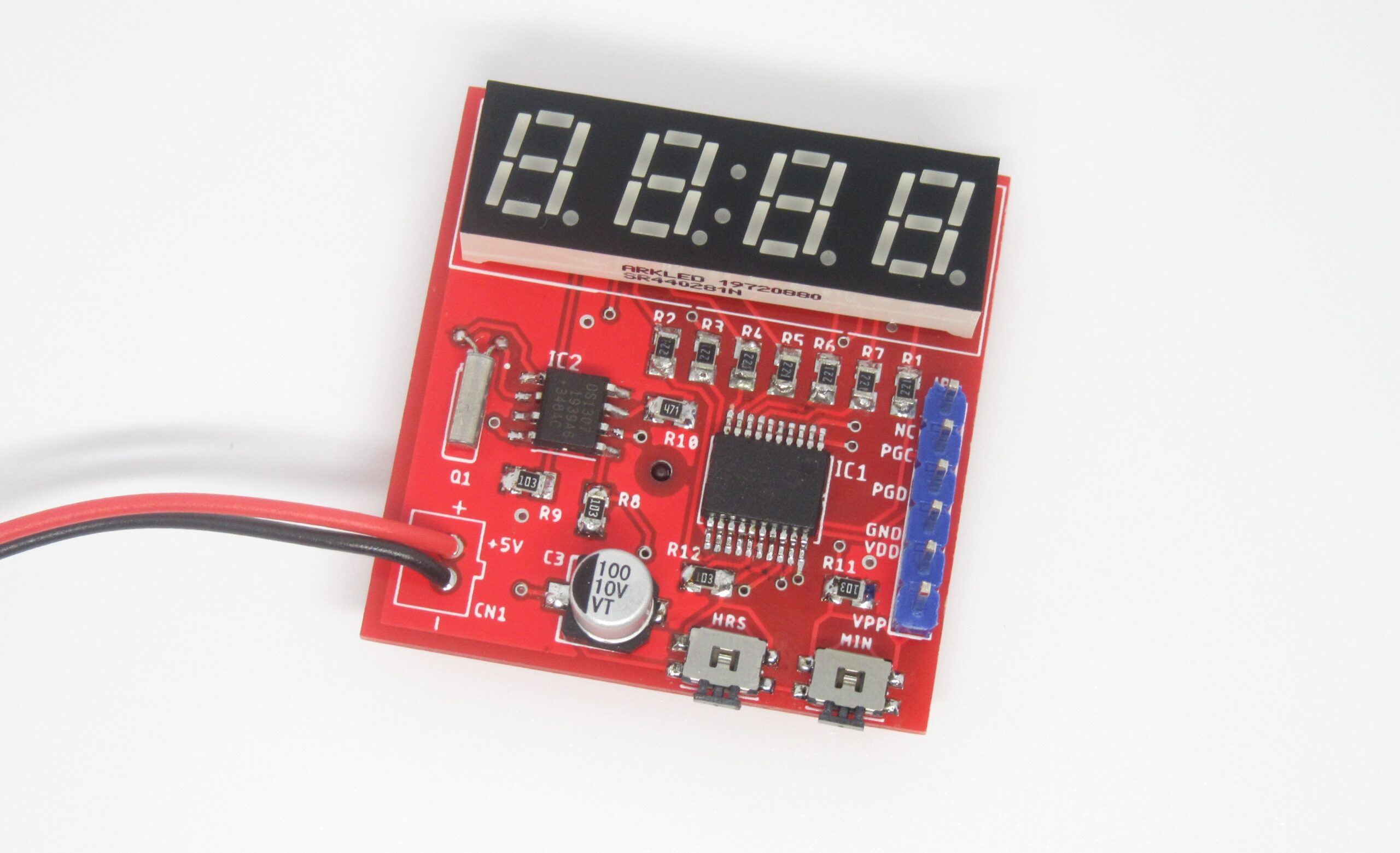
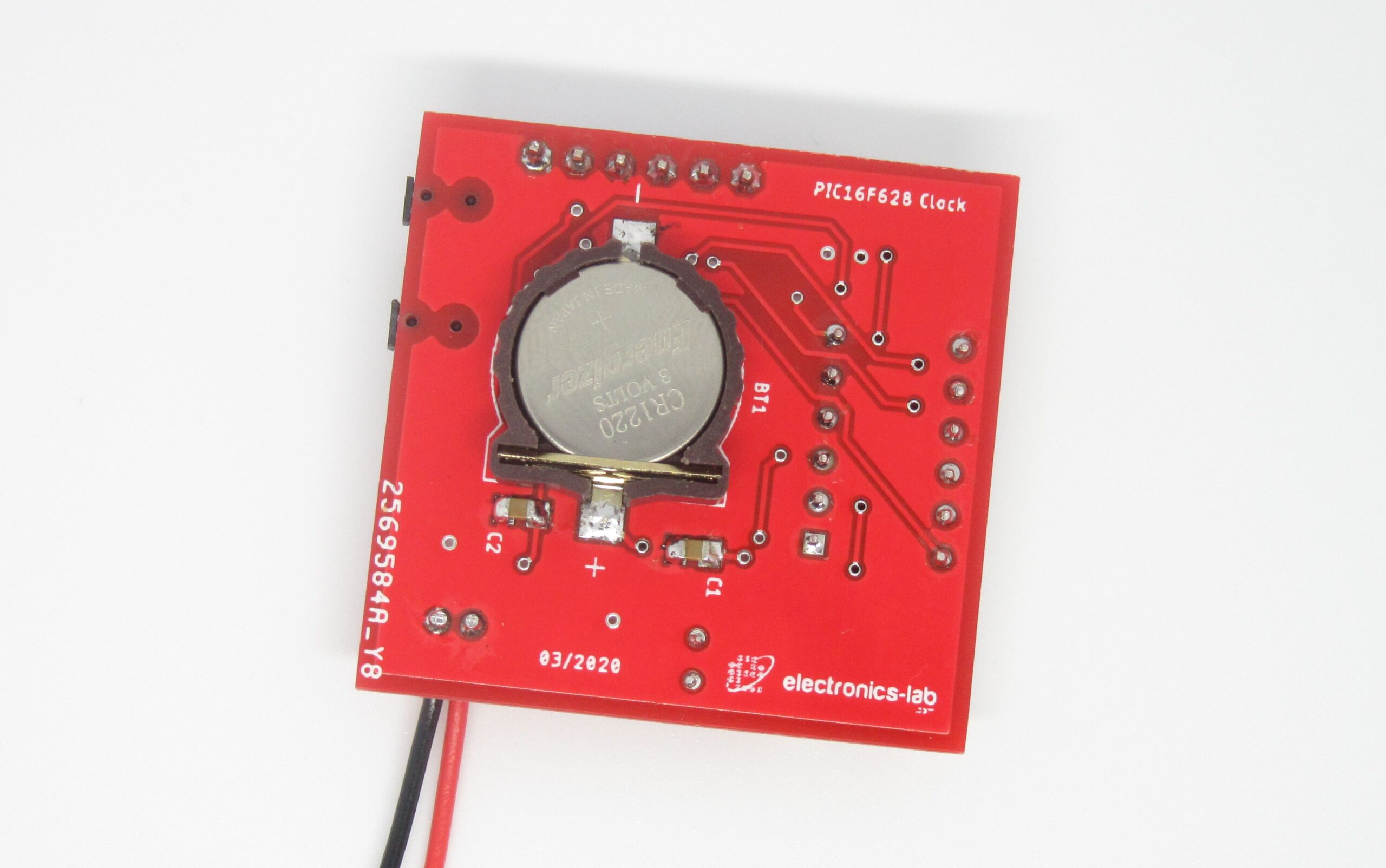
This is a minimal and small clock based on PIC16F628A microcontroller and DS1307 RTC IC. It is able to only show the time on a small 7-segment display with a total of 4 segments. The display we used is a 0.28″ SR440281N RED common cathode display bought from LCSC.com, but you can use other displays as well such as the 0.56″ Kingbright CC56-21SRWA. This project is heavily inspired by the “Simple Digital Clock with PIC16F628A and DS1307” in the case of schematic and we also used the same .hex as”Christo”.
Schematic
The schematic is straight forward. The heart is the PIC16F628A microcontroller running on the internal 4MHz oscillator, so no external crystal is needed. This saves us 2 additional IOs. The RESET Pin (MCLR) is also used as input for one of the buttons. All display segments are connected to PORTB and COMs are connected to PORTA. The RTC chip is also connected to PORTA using the I2C bus.
The refresh rate of the digits is about 53Hz and there is no visible flickering. The display segments are time-multiplexed and this makes them appear dimmer than the specifications. To compensate we are going to use some low resistors on the anodes. “Christo” tested it with different values for current limiting resistors R1-R7 and below 220Ω the microcontroller starts to misbehave (some of the digits start to flicker) above 220 Ohm everything seems OK. On the display we used the two middle dots are not connected to any pin on the package, so for the seconds’ indicators, we used the “comma” dots. These pins are connected to the SQW pin of the DS1307, which provides a square wave output with 1 sec period. The SQW pin is open drain, so we need to add a pull-up resistor. Τhe value of this resistor is chosen at 470Ω, after some trial and error testing. On the input side of the MCU, there are two buttons for adjusting the MINUTES and HOURS of the clock as indicated on the schematic. Onboard there is also an ICSP Programming connector, to help with the firmware upload. Finally, there is one unused pin left (RB7), which can be used for additional functionality, like adding a buzzer or an additional LED.
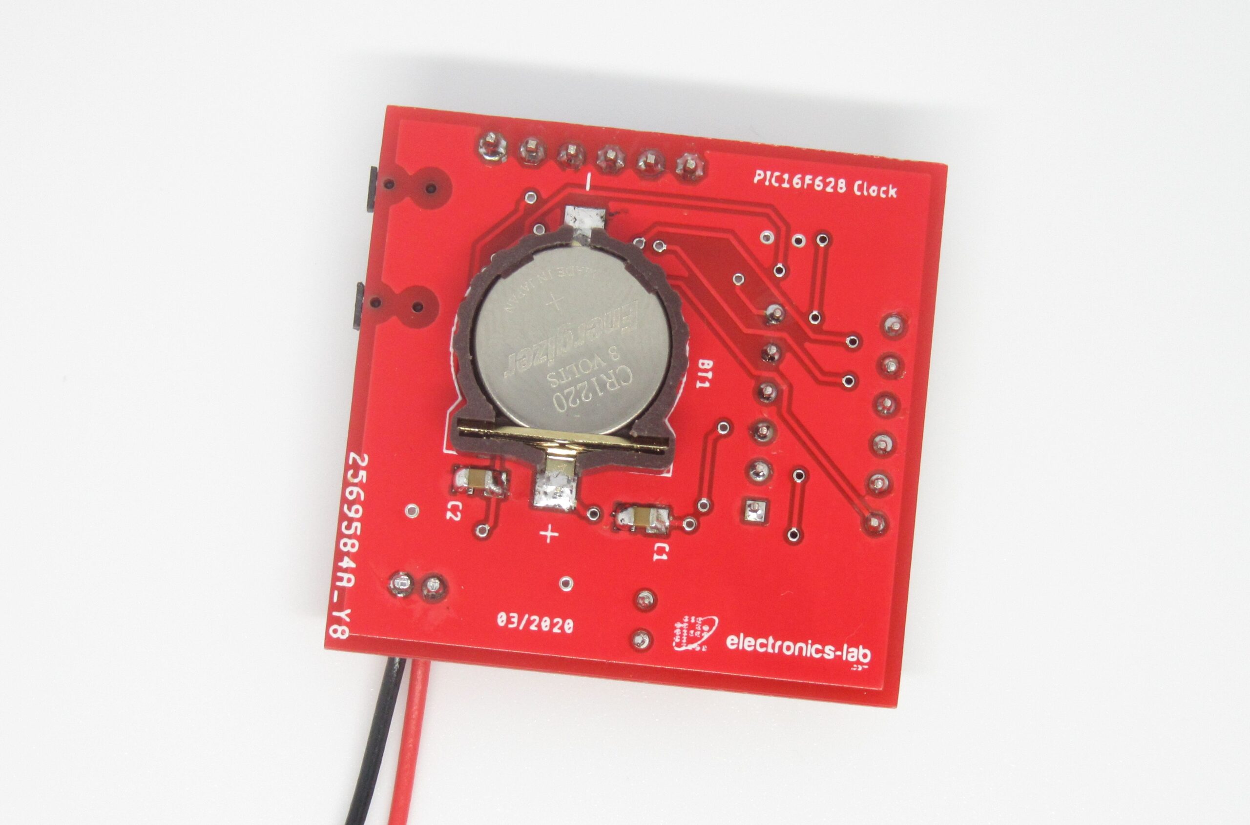
The DS1307 RTC needs an external crystal to keep the internal clock running and a backup battery to keep it running while the main power is OFF. So, the next time you power ON the clock the time would be current. To keep the overall board dimensions small we used a CR1220 battery holder with the appropriate 3V battery. Power consumption is about 35-40mA @ 5V input.
Code
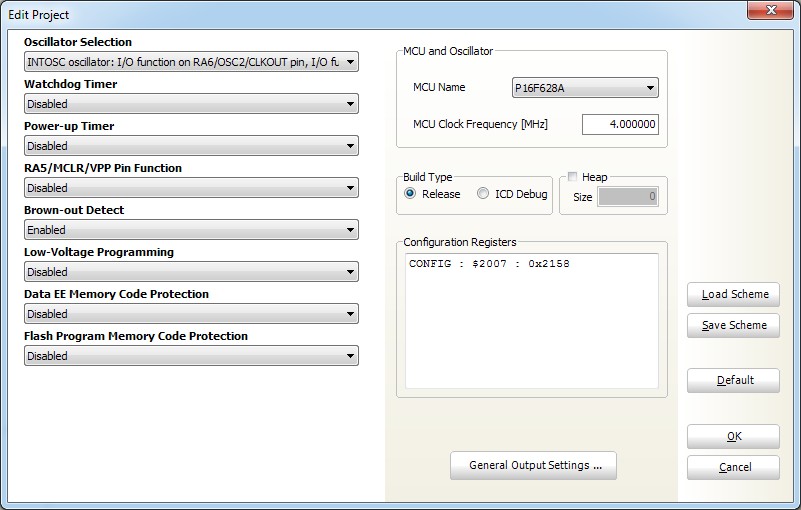
According to the author, the code is written and compiled with MikroC Pro and uses the build-in software I2C library for communicating with RTC chip. If you want to use MPLAB IDE for compiling the code you should write your own I2C library from scratch. For programming the board we used PICkit 3 programmer and software. In this case, in the “Tools” menu check the option “Use VPP First Program Entry“.
PIC Programmer Configuration
The code for this project is listed below. Additionally, you will need the “Digital Clock (PIC16F628A, DS1307, v2).h” file which can be found on the .zip in downloads below. Compiled .hex file is also provided on the same .zip file.
#include "Digital Clock (PIC16F628A, DS1307, v2).h"
#define b1 RA6_bit
#define b2 RA5_bit

// b1_old, b2_old - old state of button pins
// hour10, hour1 - tens and ones of the hour
// min10, min1 = tens and ones of the minutes
byte b1_old, b2_old, hour1, hour10, min1, min10;

// definitions for Software_I2C library
sbit Soft_I2C_Scl           at RA0_bit;
sbit Soft_I2C_Sda           at RA7_bit;
sbit Soft_I2C_Scl_Direction at TRISA0_bit;
sbit Soft_I2C_Sda_Direction at TRISA7_bit;


//  correct bits for each digit
//     RB6 RB5 RB4 RB3 RB2 RB1 RB0
//     g   f   e   d   c   b   a
//  0: 0   1   1   1   1   1   1   0x3F
//  1: 0   0   0   0   1   1   0   0x06
//  2: 1   0   1   1   0   1   1   0x5B
//  3: 1   0   0   1   1   1   1   0x4F
//  4: 1   1   0   0   1   1   0   0x66
//  5: 1   1   0   1   1   0   1   0x6D
//  6: 1   1   1   1   1   0   1   0x7D
//  7: 0   0   0   0   1   1   1   0x07
//  8: 1   1   1   1   1   1   1   0x7F
//  9: 1   1   0   1   1   1   1   0x6F
// BL: 0   0   0   0   0   0   0   0x00

const byte segments[11] = {0x3F, 0x06, 0x5B, 0x4F, 0x66, 0x6D, 0x7D, 0x07, 0x7F, 0x6F, 0x00};


//***********************************************//
//   Sets read or write mode at select address   //
//***********************************************//
void DS1307_Select(byte Read, byte address) {
     Soft_I2C_Start();
     Soft_I2C_Write(0xD0);       // start write mode
     Soft_I2C_Write(address);    // write the initial address
     if (Read) {
        Soft_I2C_Stop();
        Soft_I2C_Start();
        Soft_I2C_Write(0xD1);    // start read mode
     }
}

//********************************//
//   Initialize the DS1307 chip   //
//********************************//
void DS1307_Init() {
     byte sec, m, h;
     DS1307_Select(1, 0);                 // start reading at address 0
     sec = Soft_I2C_Read(1);              // read seconds byte
     m = Soft_I2C_Read(1);                // read minute byte
     h = Soft_I2C_Read(0);                // read hour byte
     Soft_I2C_Stop();
     if (sec > 127) {                     // if the clock is not running  (bit 7 == 1)
        DS1307_Select(0, 0);              // start writing at address 0
        Soft_I2C_Write(0);                // start the clock (bit 7 = 0)
        Soft_I2C_Stop();
        DS1307_Select(0, 7);              // start writing at address 7
        Soft_I2C_Write(0b00010000);       // enable square wave output 1 Hz
        Soft_I2C_Stop();
     }
     m = (m >> 4)*10 + (m & 0b00001111);  // converting from BCD format to decimal
     if (m > 59) {
        DS1307_Select(0, 1);              // start writing at address 1
        Soft_I2C_Write(0);                // reset the minutes to 0
        Soft_I2C_Stop();
     }
     if (h & 0b01000000) {                // if 12h mode (bit 6 == 1)
        if (h & 0b00100000)               // if PM (bit 5 == 1)
           h = 12 + ((h >> 4) & 1)*10 + (h & 0b00001111);
        else
           h = ((h >> 4) & 1)*10 + (h & 0b00001111);
     }
     else
        h = ((h >> 4) & 3)*10 + (h & 0b00001111);
     if (h > 23) {
        DS1307_Select(0, 2);              // start writing at address 2
        Soft_I2C_Write(0);                // reset the hours to 0 in 24h mode
        Soft_I2C_Stop();
     }
}


void incrementH() {     // increments hours and write it to DS1307
     hour1++;
     if ((hour10 < 2 && hour1 > 9) || (hour10 == 2 && hour1 > 3)) {
        hour1 = 0;
        hour10++;
        if (hour10 > 2)
           hour10 = 0;
     }
     DS1307_Select(0, 2);
     Soft_I2C_Write((hour10 << 4) + hour1);
     Soft_I2C_Stop();
}


void incrementM() {     // increments minutes and write it to DS1307
     min1++;
     if (min1 > 9) {
        min1 = 0;
        min10++;
        if (min10 > 5)
           min10 = 0;
     }
     DS1307_Select(0, 0);
     Soft_I2C_Write(0);                       // reset seconds to 0
     Soft_I2C_Write((min10 << 4) + min1);     // write minutes
     Soft_I2C_Stop();
}

void main(){
     // pos: current digit position;
     // counter1, counter2: used as flag and for repeat functionality for the buttons
     // COM[]: drive the common pins for the LED display
     byte pos, counter1, counter2, COM[4] = {0b11101111, 0b11110111, 0b11111011, 0b11111101};
     CMCON = 0b00000111;             // comparator off
     TRISA = 0b01100000;
     TRISB = 0b00000000;
     b1_old = 1;
     b2_old = 1;
     counter1 = 0;
     counter2 = 0;
     pos = 0;
     Soft_I2C_Init();
     DS1307_Init();
     while (1) {
           DS1307_Select(1, 1);      // select reading at address 1
           min1 = Soft_I2C_Read(1);  // read minutes byte
           hour1 = Soft_I2C_Read(0); // read houts byte
           Soft_I2C_Stop();
           min10 = min1 >> 4;
           min1 = min1 & 0b00001111;
           hour10 = hour1 >> 4;
           hour1 = hour1 & 0b00001111;
           if (b1 != b1_old) {        // if the button1 is pressed or released
              b1_old = b1;
              counter1 = 0;
           }
           if (!b1_old) {             // if the button1 is pressed
              if (counter1 == 0)
                 incrementH();        // increment hour
              counter1++;
              if (counter1 > 50)      // this is repeat functionality for the button1
                 counter1 = 0;
           }
           if (b2 != b2_old) {        // if the button2 is pressed or released
              b2_old = b2;
              counter2 = 0;
           }
           if (!b2_old) {             // if the button2 is pressed
              if (counter2 == 0)
                 incrementM();        // increment minutes and reset the seconds to 0
              counter2++;
              if (counter2 > 50)      // this is repeat functionality for the button2
                 counter2 = 0;
           }

           TRISA = TRISA | 0b00011110;       // set all 4 pins as inputs
           switch (pos) {                    // set proper segments high
             case 0: PORTB = segments[hour10]; break;
             case 1: PORTB = segments[hour1]; break;
             case 2: PORTB = segments[min10]; break;
             case 3: PORTB = segments[min1]; break;
           }
           TRISA = TRISA & COM[pos];         // set pin at current position as output
           PORTA = PORTA & COM[pos];         // set pin at current position low
           pos++;                            // move to next position
           if (pos > 3) pos = 0;
     }
}
PCB
PCB is designed with Autodesk EAGLE and design files are available in downloads below. The overall dimensions of the board are 35.56 x 36.61 mm and we used almost SMD components.
Spare PCBs are available for shipment around the world. If you would like to get some drop us a line.
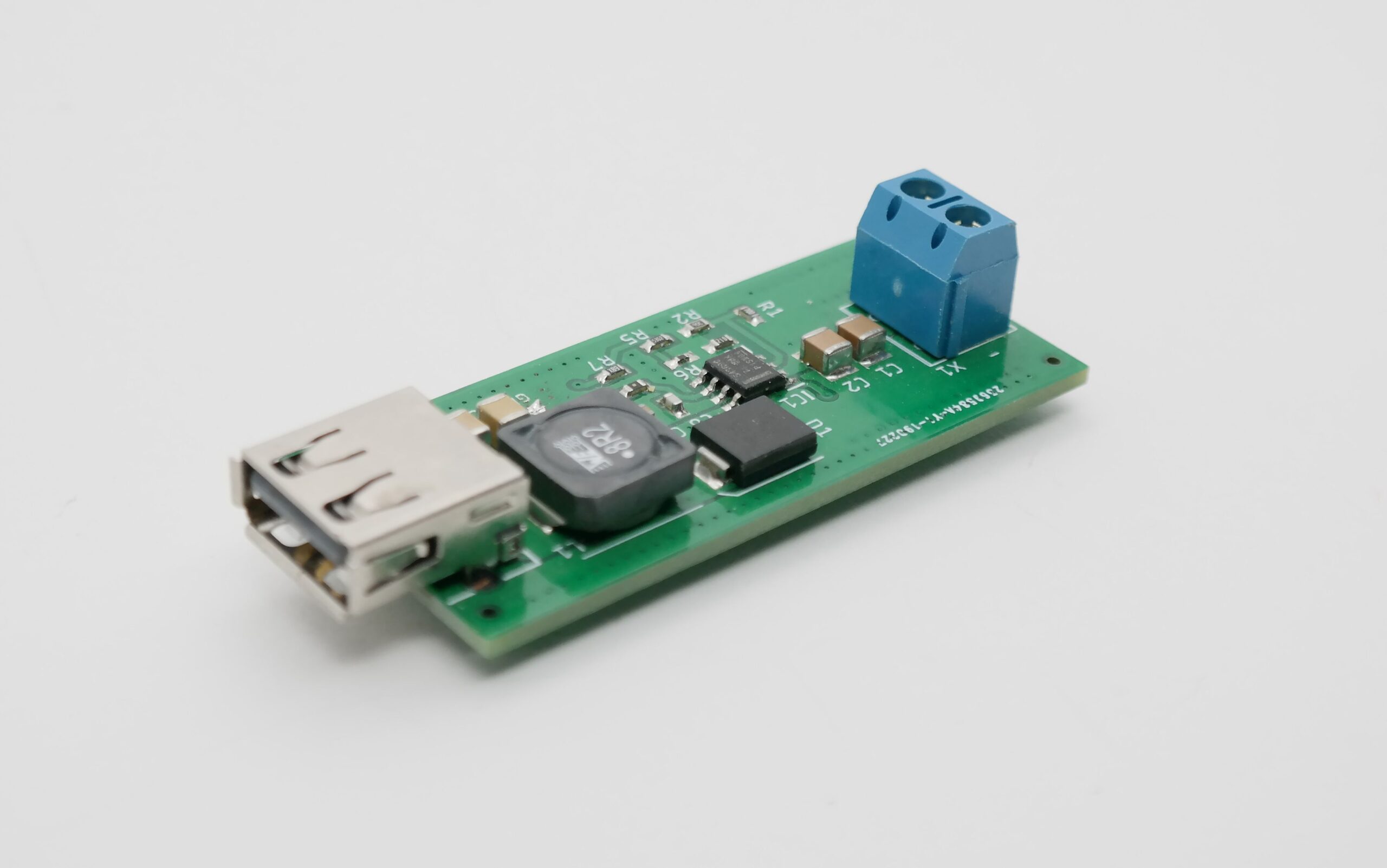
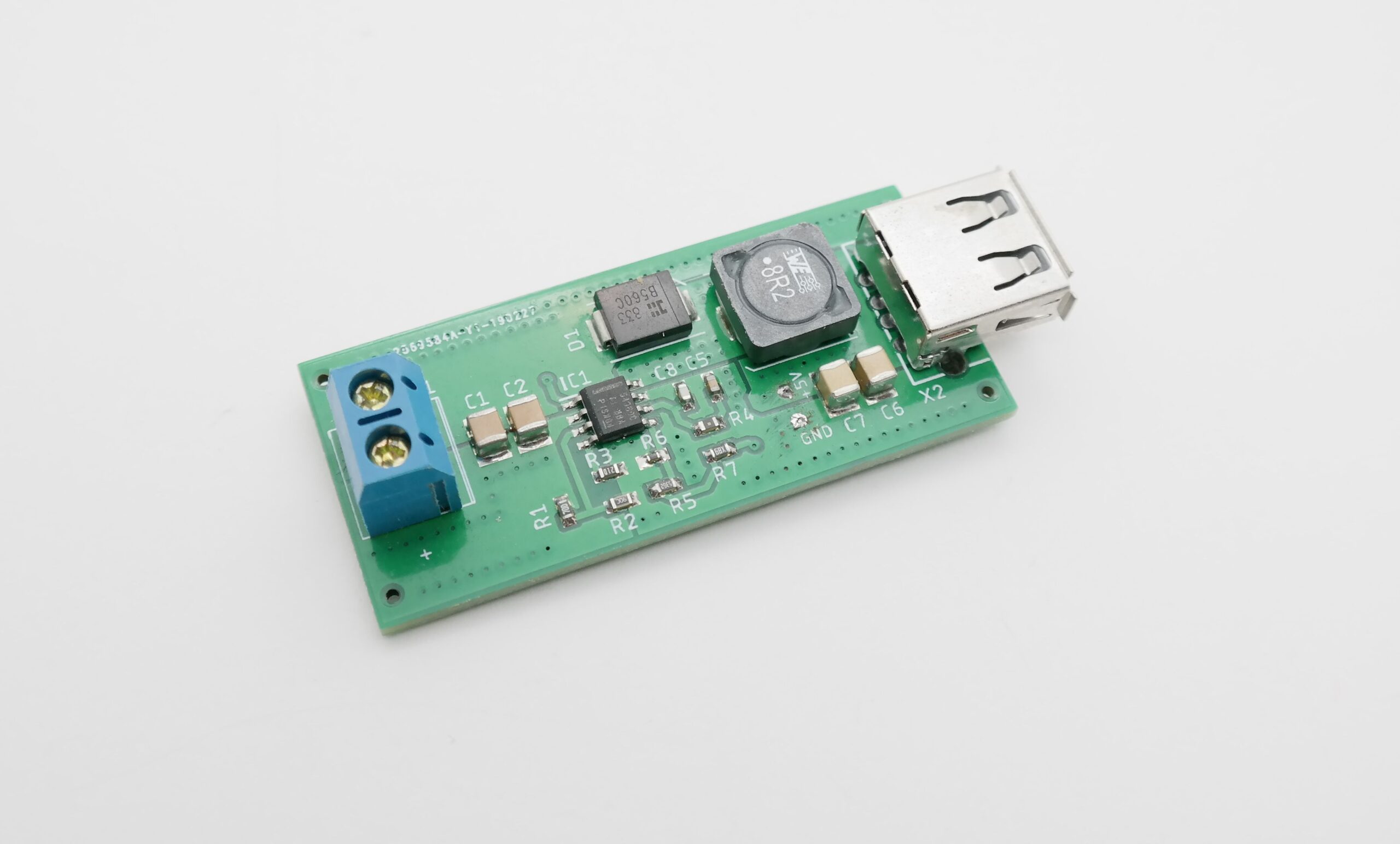
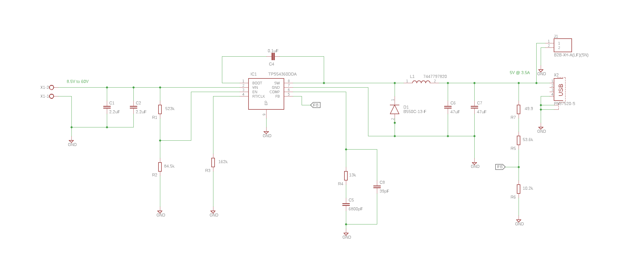
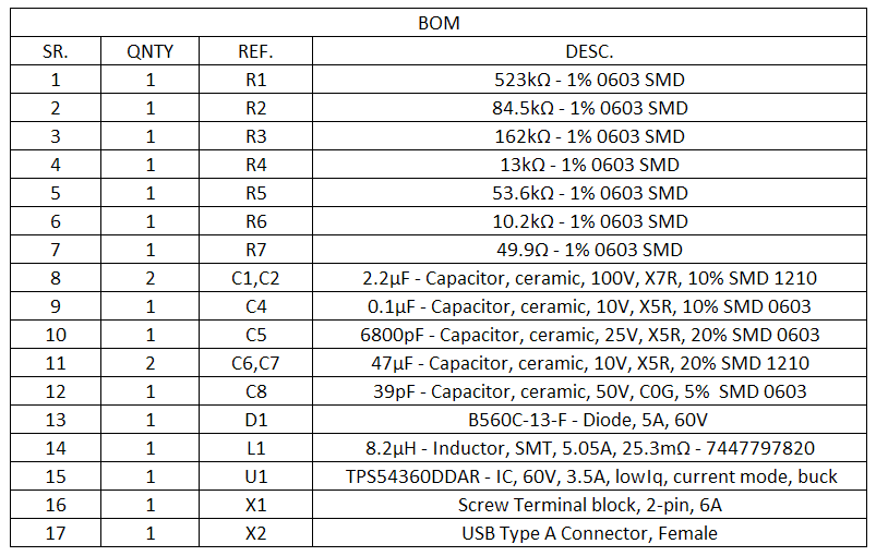
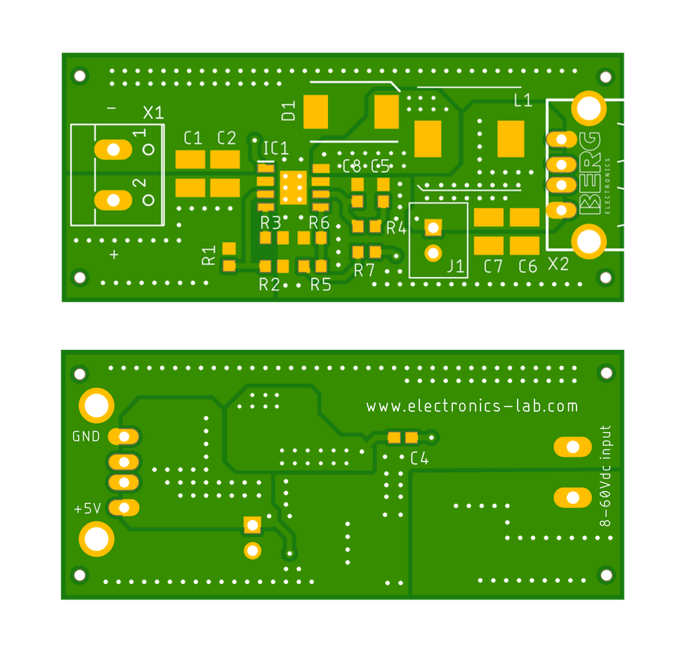
This is a 60V to 5V – 3.5A step down DC-DC converter based on TPS54360B from Texas Instruments. Sample applications are: 12 V, 24 V and 48 V industrial, Automotive and Communications Power Systems. The TPS54360 is a 60V, 3.5A, step down regulator with an integrated high side MOSFET. The device survives load dump pulses up to 65V per ISO 7637. Current mode control provides simple external compensation and flexible component selection. A low ripple pulse skip mode reduces the no load supply current to 146 μA. Shutdown supply current is reduced to 2 μA when the enable pin is pulled low.
Under-voltage lockout is internally set at 4.3 V but can be increased using the enable pin. The output voltage start up ramp is internally controlled to provide a controlled start up and eliminate overshoot. A wide switching frequency range allows either efficiency or external component size to be optimized. Frequency fold back and thermal shutdown protects internal and external components during an overload condition.
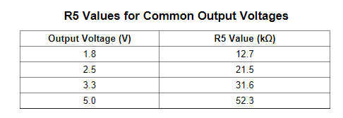
Note: The output voltage is set by a resistor divider from the output node to the FB terminal. It is recommended to use 1% tolerance or better divider resistors, choose R5, R6 for other output voltages.
It is strongly recommended to use adequate air flow over the board to ensure it doesn’t go at thermal shutdown. See thermal profile below.
Setting Output Voltage
The following table lists the R5 values for some common output voltages assuming R6= 10.0kΩ
Features
Supply Input 8.5V-60V
Output 5V (Output Voltage adjustable with R5, R6)
Output Current 3.5A
100 kHz to 2.5 MHz Switching Frequency
Optional JST connector for 5V Fan
Current Mode Control DC-DC Converter
Integrated 90-mΩ High Side N-Channel MOSFET
High Efficiency at Light Loads with Pulse Skipping Eco-mode™
Low Dropout at Light Loads with Integrated BOOT Recharge FET
146 μA Operating Quiescent Current
1 µA Shutdown Current
Internal Soft-Start
Accurate Cycle-by-Cycle Current Limit
Thermal, Overvoltage, and Frequency Fold back Protection
PCB Dimensions 55.50mm x 24.64mm
Schematic
Parts List
PCB
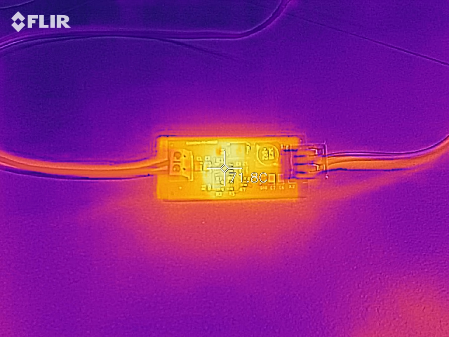
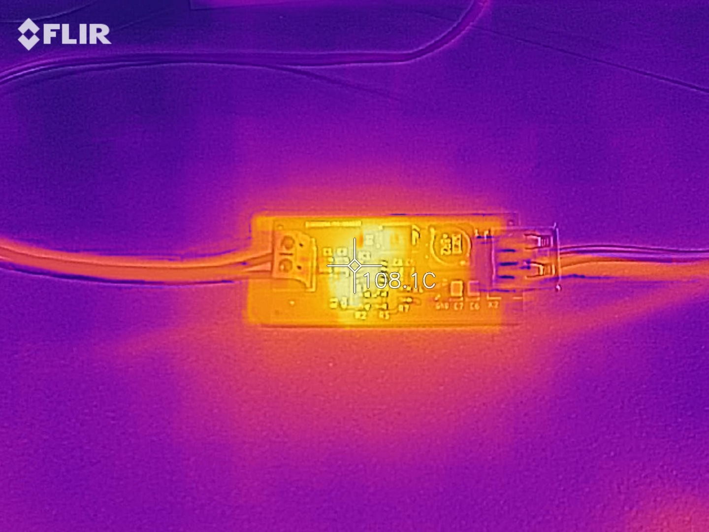
Thermal Image
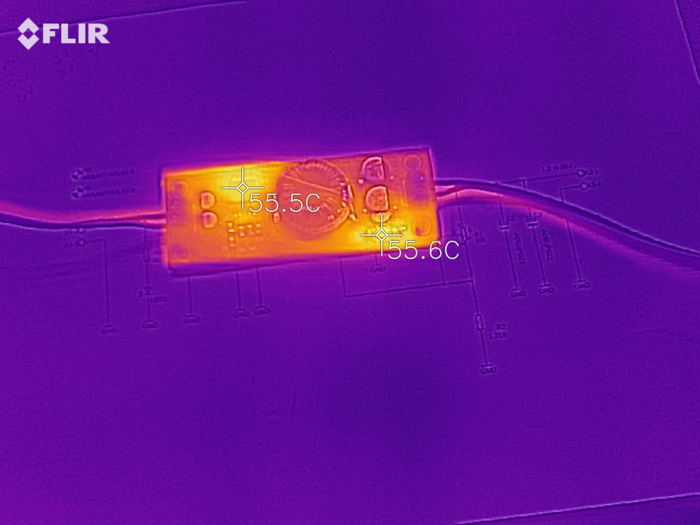
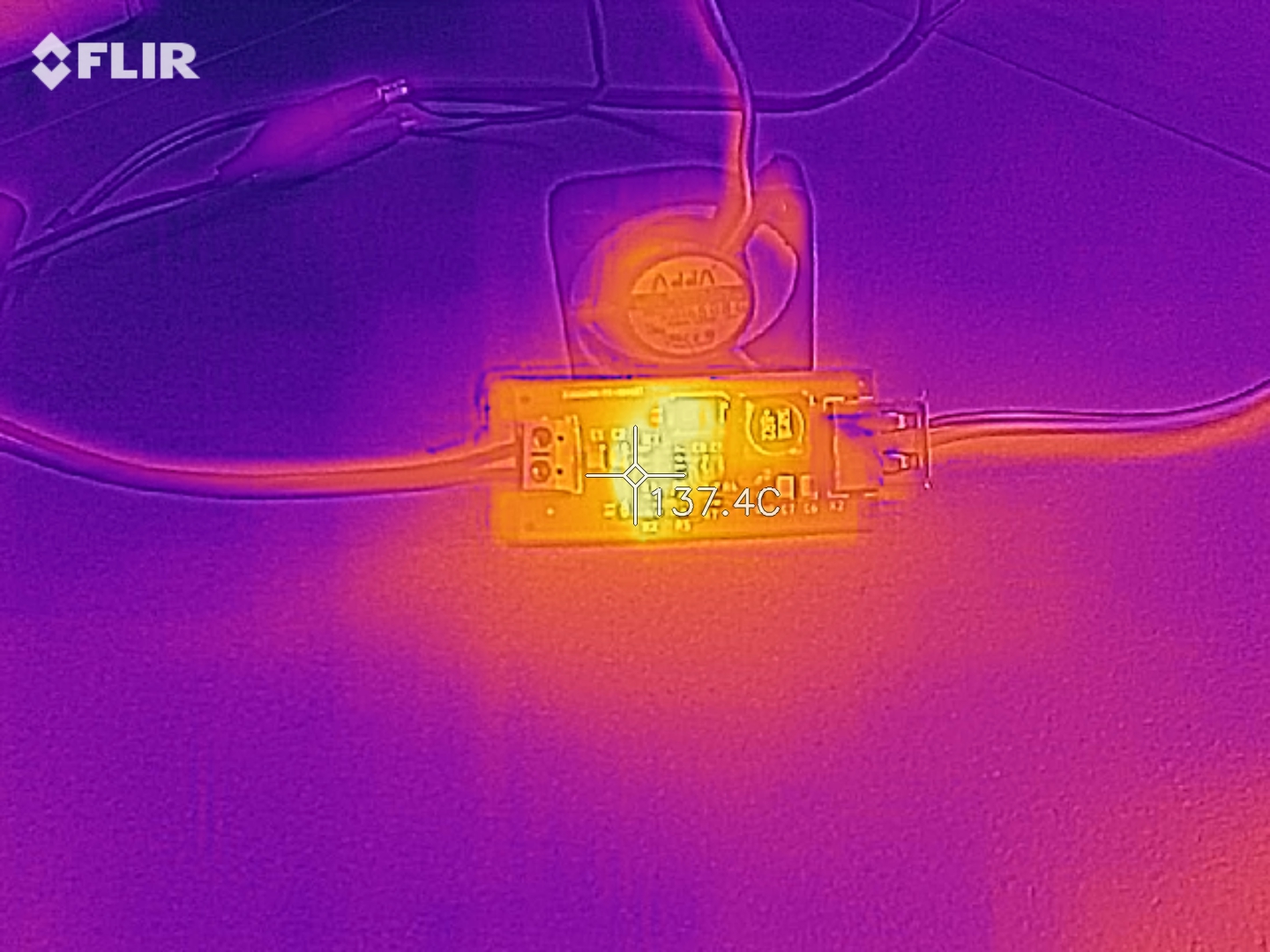
You can see on the thermal images below that at 60V input – 5V @2A output the IC gets too hot (>105ºC) and if we go for higher outputs (2.5-3A) the IC gets in thermal cut-off. To avoid this situation you can use a small 5V FAN to blow air on the board or probably use a heatsink attached to the board.
60V input – 5V @1A output60V input – 5V @2A output60V input – 5V @3A output cooled with a small FAN
Measurements
The efficiency is calculated based on the (Pout/Pin)*100%. For 60V input and 5V @3A output the input current is 0.32A, so Pin=19.38W. Pout=5V*3A=15W, so e=77.39% with Pdis = 4.58W
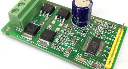
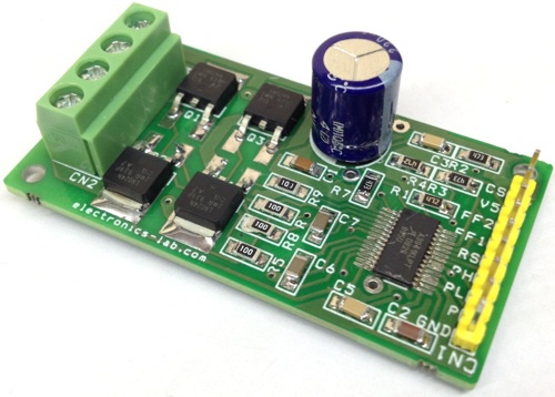
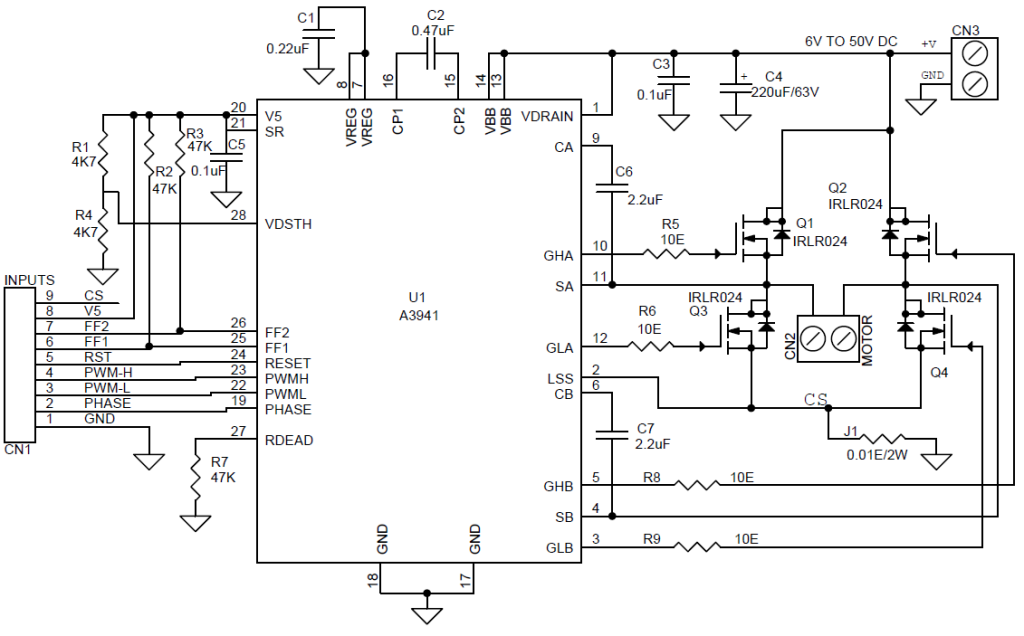
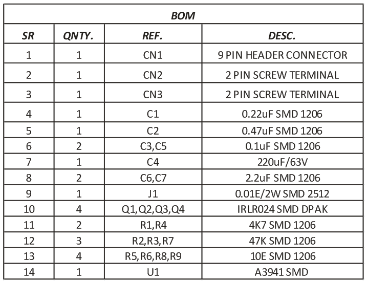
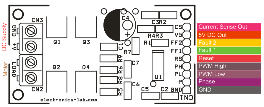
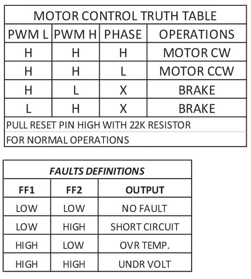
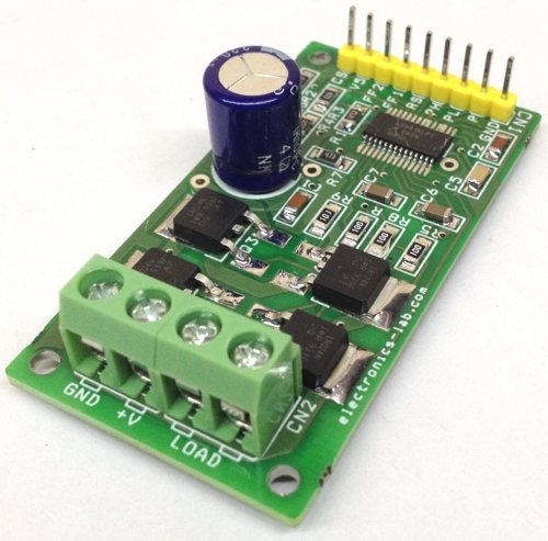
This tiny board is designed to drive a bidirectional DC brushed motor of large current. DC supply is up to 50V DC. A3941 gate driver IC and 4X N Channel Mosfet IRLR024 used as H-Bridge. The project can handle a load of up to 10A. Screw terminals are provided to connect the load and load supply, and 9 Pin header connector is provided for easy interface with the microcontroller. An on board, shunt resistor provides current feedback.
The A3941 is a full-bridge controller for use with external N-channel power MOSFETs and is specifically designed for automotive applications with high-power inductive loads, such as brush DC motors. A unique charge pump regulator provides full (>10 V) gate drive for battery voltages down to 7 V and allows the A3941 to operate with a reduced gate drive, down to 5.5 V. A bootstrap capacitor is used to provide the above-battery supply voltage required for N-channel MOSFETs. An internal charge pump for the high-side drive allows DC (100% duty cycle) operation.
The full bridge can be driven in fast or slow decay modes using diode or synchronous rectification. In the slow decay mode, current recirculation can be through the high-side or the low side FETs. The power FETs are protected from shoot-through by resistor R7 adjustable dead time. Integrated diagnostics provide an indication of under voltage, over temperature, and power bridge faults, and can be configured to protect the power MOSFETs under most short circuit conditions.
The A3941 is a full-bridge MOSFET driver (pre-driver) requiring a single unregulated supply of 7 to 50 V. It includes an integrated 5 V logic supply regulator. The four high current gate drives are capable of driving a wide range of N-channel power MOSFETs, and are configured as two high-side drives and two low-side drives. The A3941 provides all the necessary circuits to ensure that the gate-source voltage of both high-side and low-side external FETs are above 10 V, at supply voltages down to 7 V. For extreme battery voltage drop conditions, correct functional operation is guaranteed at supply voltages down to 5.5 V, but with a reduced gate drive voltage. The A3941 can be driven with a single PWM input from a Microcontroller and can be configured for fast or slow decay. Fast decay can provide four-quadrant motor control, while slow decay is suitable for two-quadrant motor control or simple inductive loads. In slow decay, current recirculation can be through the high-side or the low-side MOSFETs. In either case, bridge efficiency can be enhanced by synchronous rectification. Cross conduction (shoot through) in the external bridge is avoided by an adjustable dead time. A low-power sleep mode allows the A3941, the power bridge, and the load to remain connected to a vehicle battery supply without the need for an additional supply switch. The A3941 includes a number of protection features against under voltage, over temperature, and Power Bridge faults. Fault states enable responses by the device or by the external controller, depending on the fault condition and logic settings. Two fault flag outputs, FF1 and FF2, are provided to signal detected faults to an external controller.
Features
High current gate drive for N-channel MOSFET full bridge
High-side or low-side PWM switching
Charge pump for low supply voltage operation
Top-off charge pump for 100% PWM
Cross-conduction protection with adjustable dead time
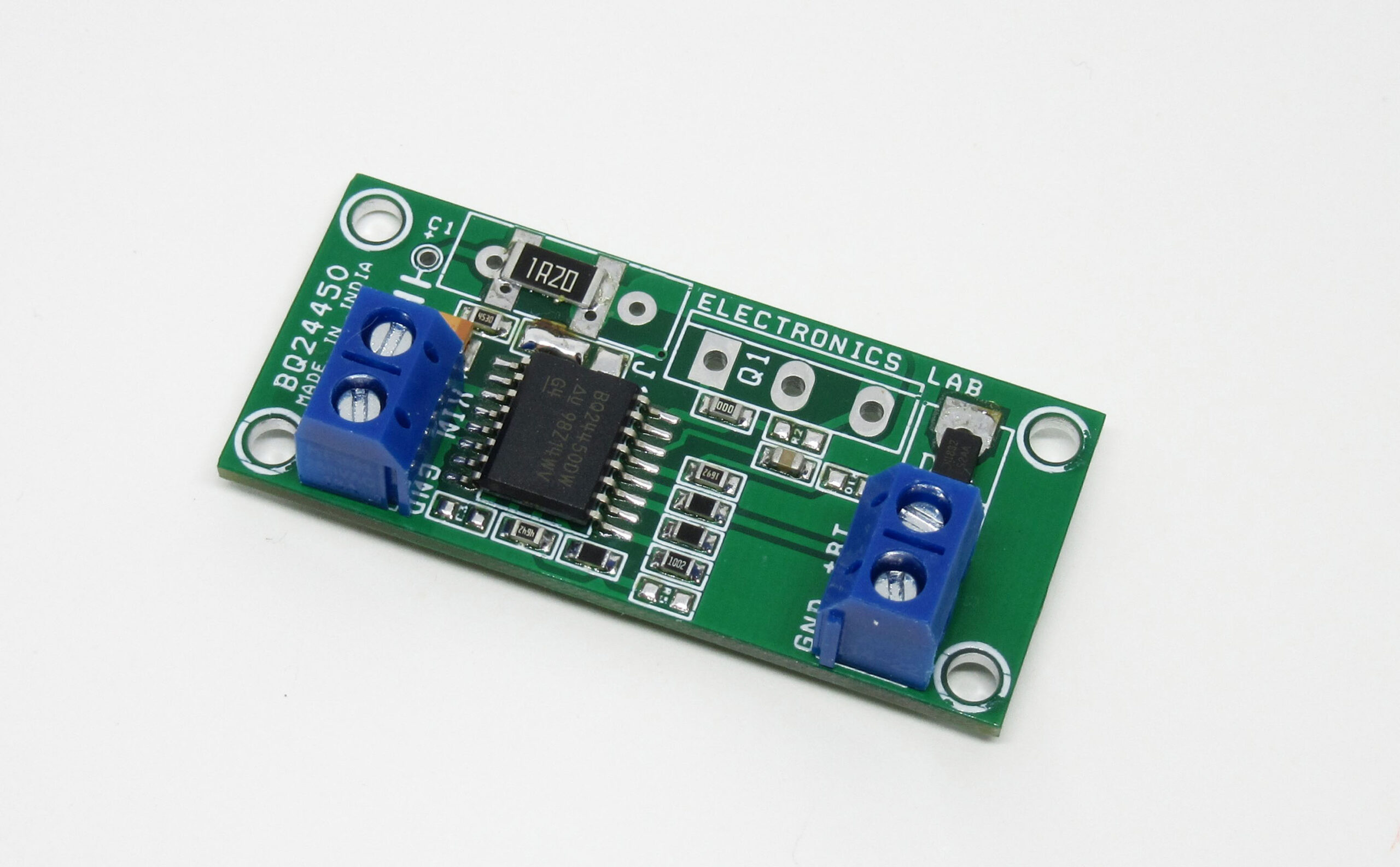
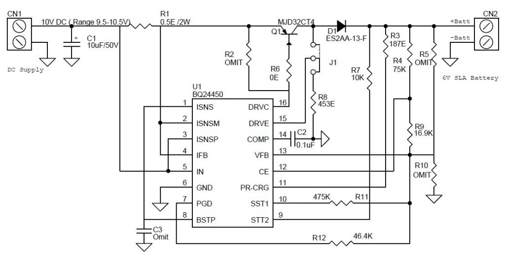
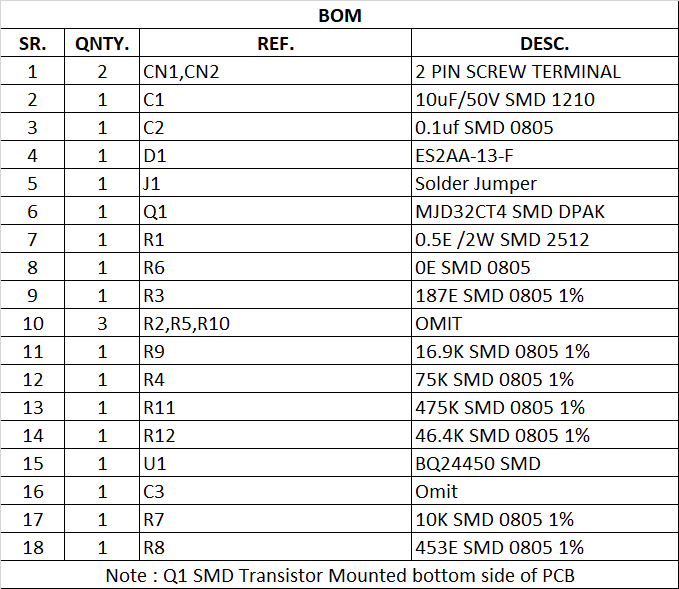
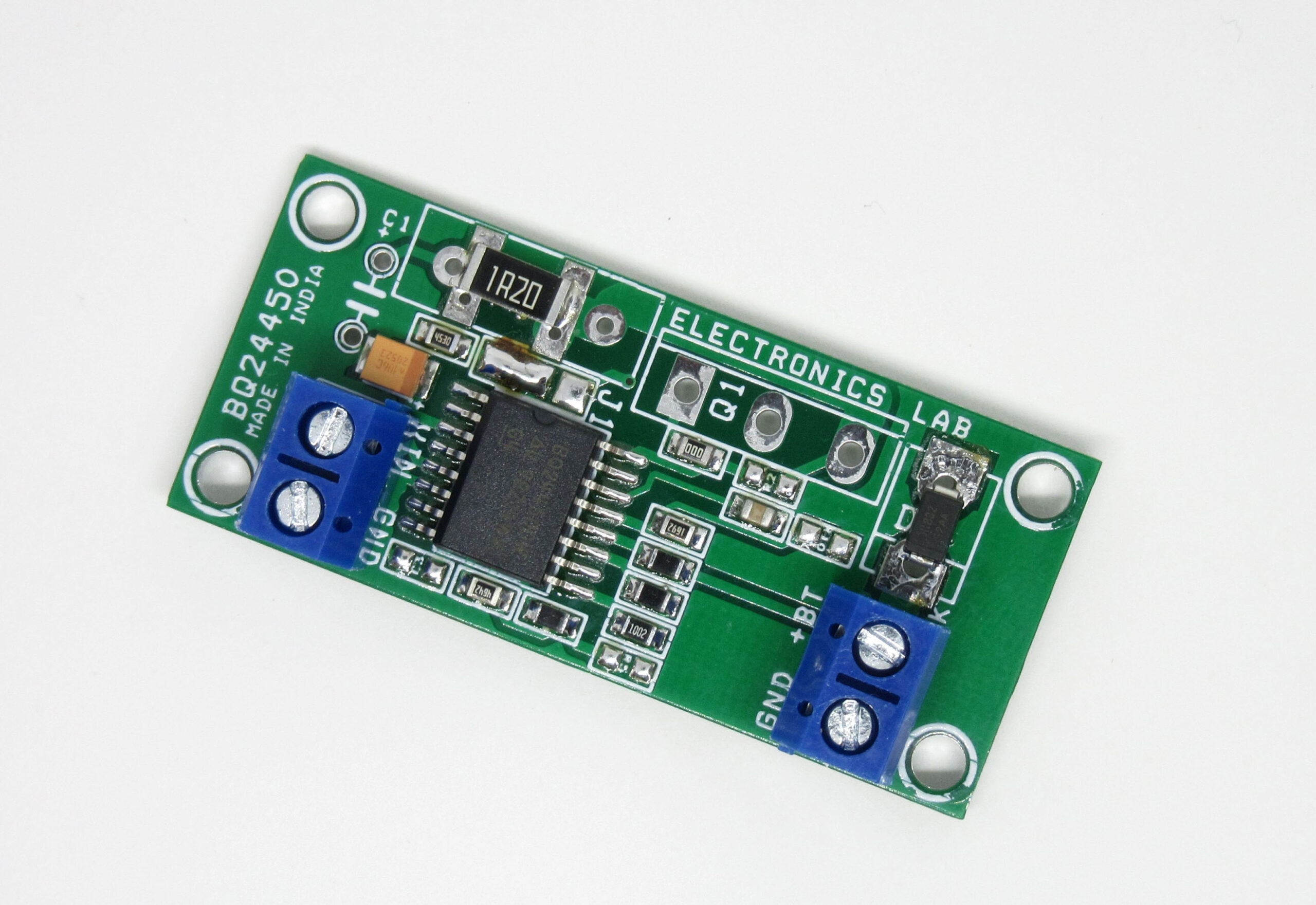
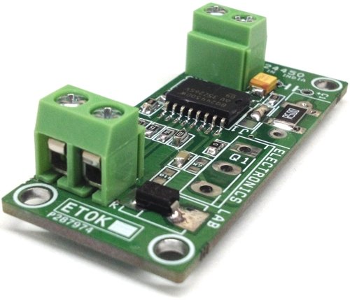
6V Lead acid (SLA) battery charger project is based on BQ24450 IC from Texas instruments. This charger takes all the guesswork out of charging and maintaining your battery, no matter what season it is. Whether you have a Bike, Robot, RC Car, Truck, Boat, RV, Emergency Light, or any other vehicle with a 6v battery, simply hook this charger maintainer up to the battery. The BQ24450 contains all the necessary circuitry to optimally control the charging of lead-acid batteries. The IC controls the charging current as well as the charging voltage to safely and efficiently charge the battery, maximizing battery capacity and life. The IC is configured as a simple constant-voltage float charge controller. The built-in precision voltage reference is especially temperature-compensated to track the characteristics of lead-acid cells, and maintains optimum charging voltage over an extended temperature range without using any external components. The low current consumption of the IC allows for accurate temperature monitoring by minimizing self-heating effects. In addition to the voltage- and current-regulating amplifiers, the IC features comparators that monitor the charging voltage and current. These comparators feed into an internal state machine that sequences the charge cycle.
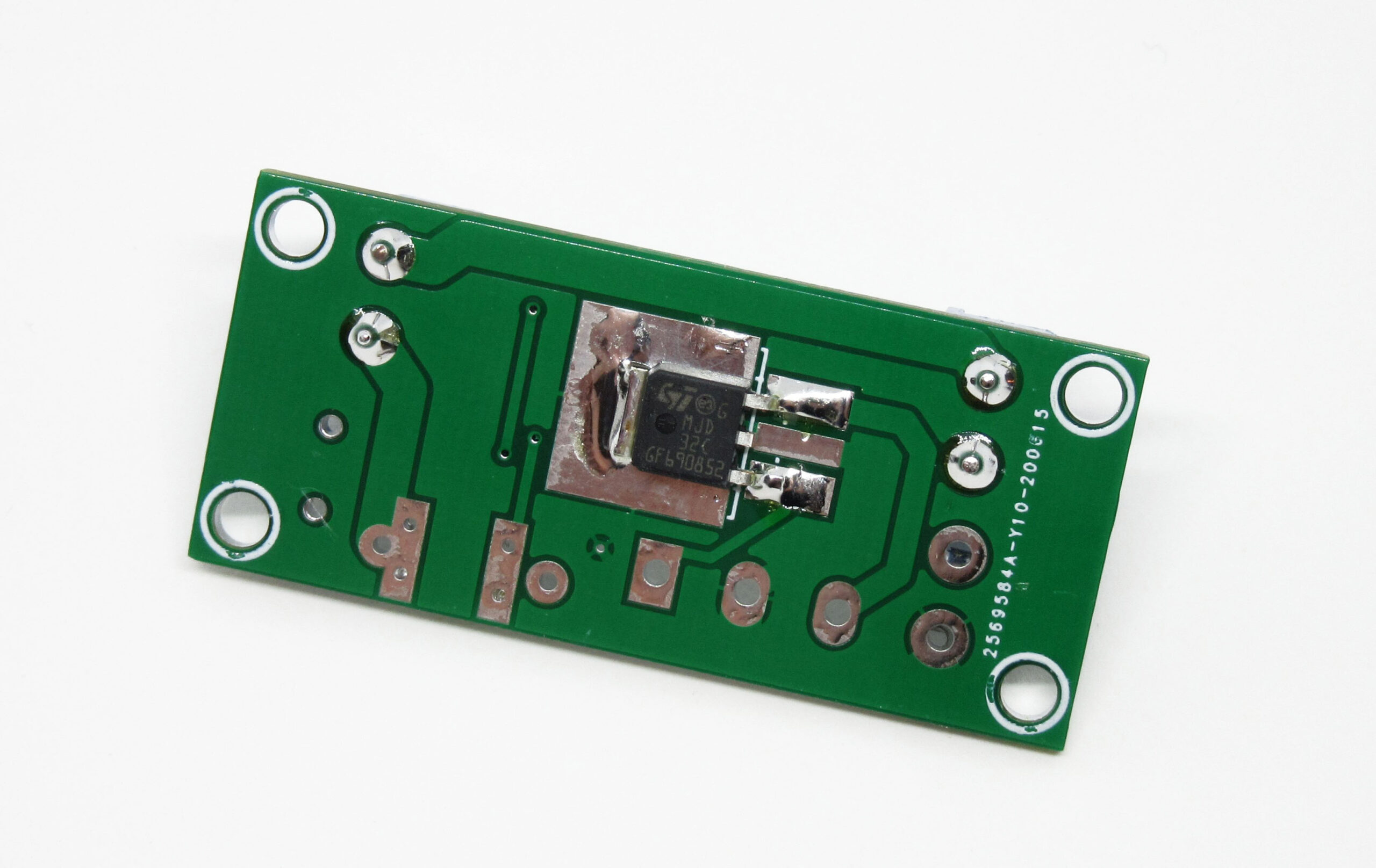
For low charging current, you can use SMD Q1 transistor on the bottom of PCB, for higher charging currents you should use a through-hole (TO247) transistor, like TIP147 on the top of PCB.
The circuit has been designed for PNP transistor (Q1) that’s why the PCB jumper is shorted to R8 by default. You can also use an NPN transistor, in this case, Omit R6, Use R2, Jumper has to be shorted the other way.
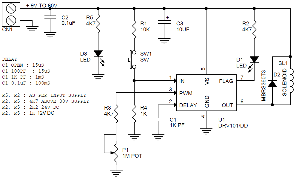
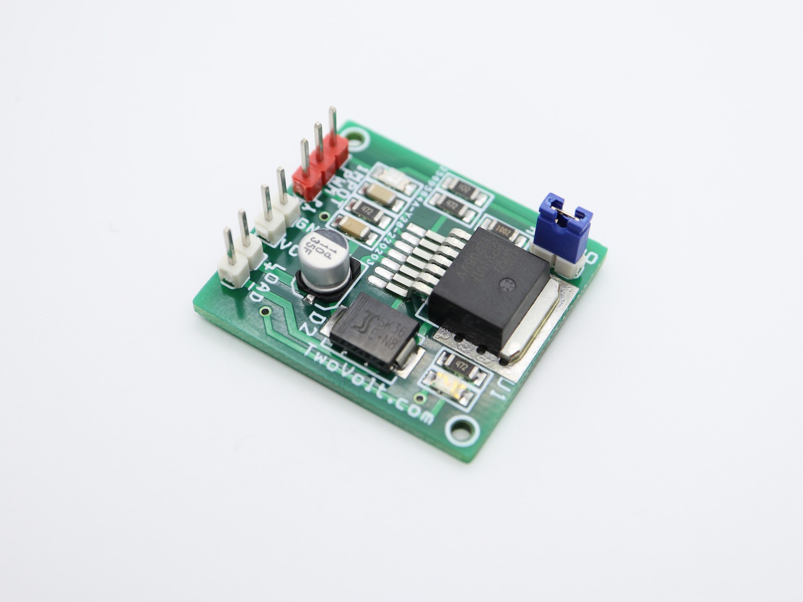
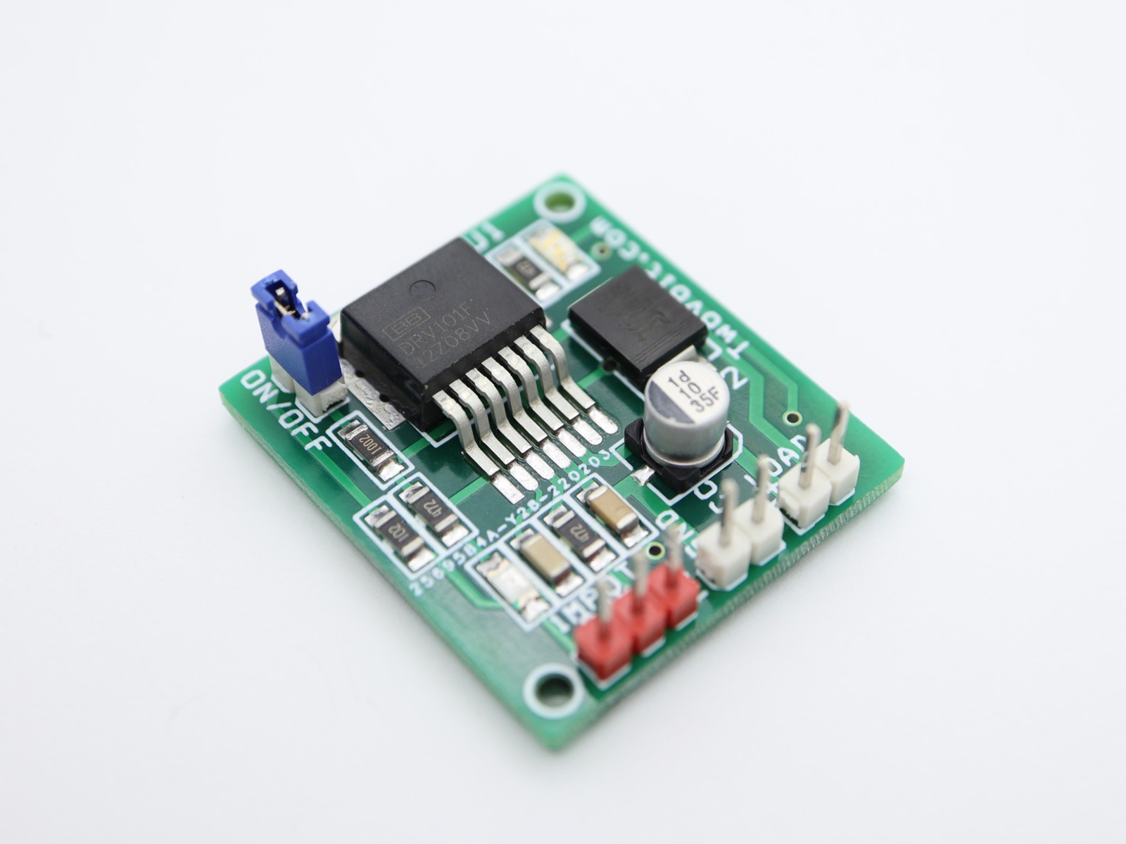
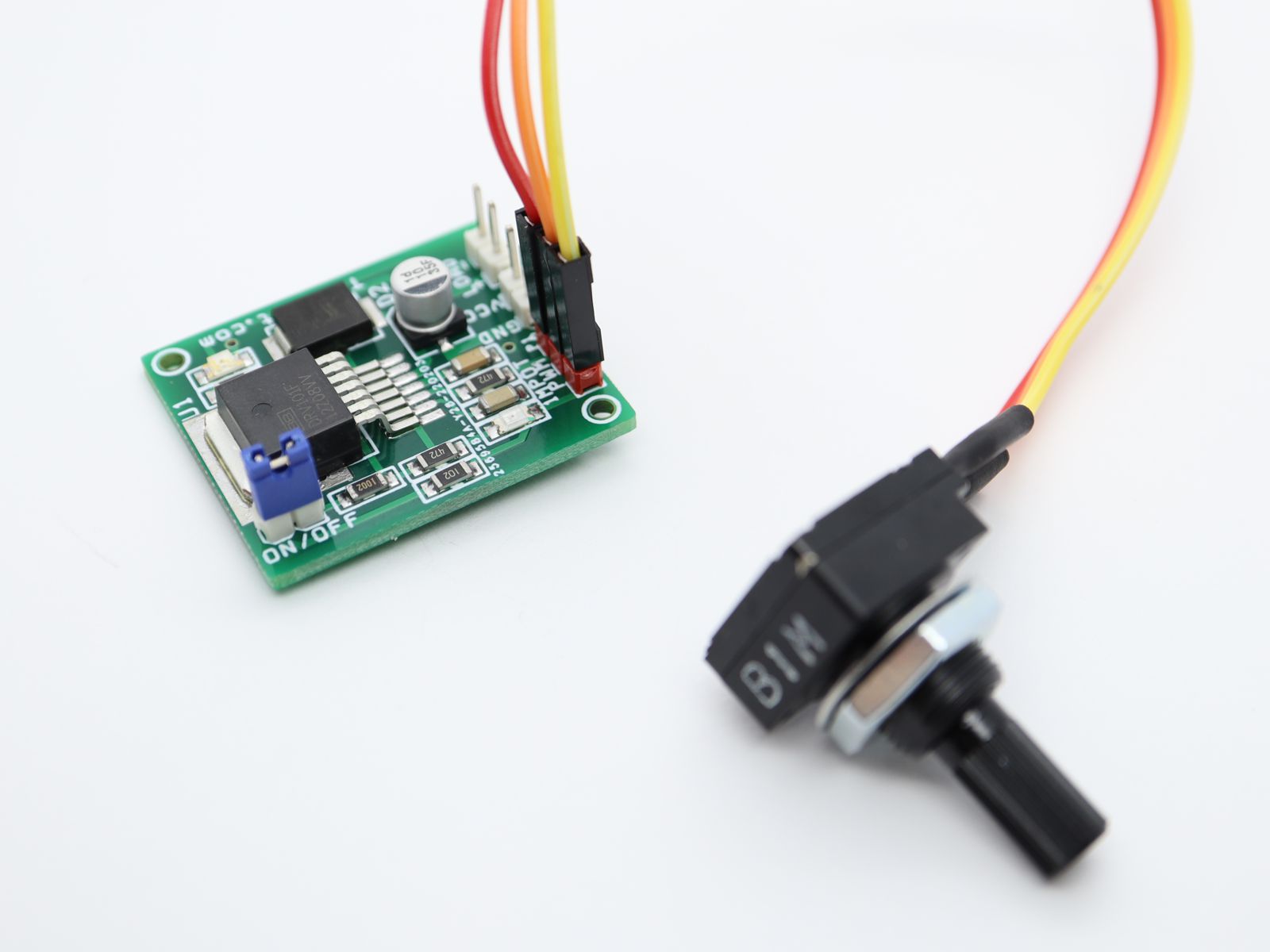
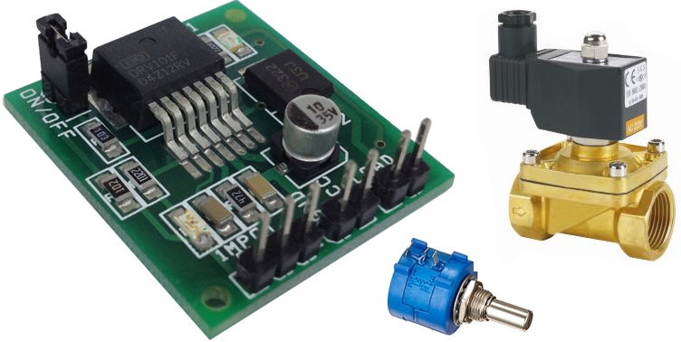
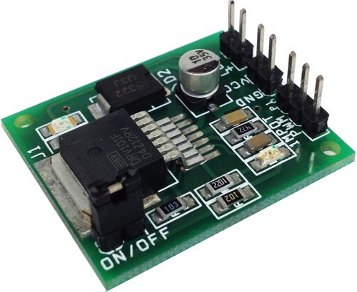
The DRV101 is a low-side power switch employing a pulse-width modulated (PWM) output. Its rugged design is optimized for driving electromechanical devices such as valves, solenoids, relays, actuators, and positioners. The DRV101 module is also ideal for driving thermal devices such as heaters and lamps. PWM operation conserves power and reduces heat rise, resulting in higher reliability. In addition, an adjustable PWM potentiometer allows fine control of the power delivered to the load. Time from dc output to PWM output is externally adjustable. The DRV101 can be set to provide a strong initial closure, automatically switching to a soft hold mode for power savings. The duty cycle can be controlled by a potentiometer, analog voltage, or digital-to-analog converter for versatility. A flag output LED D2 indicates thermal shutdown and over/under current limit. A wide supply range allows use with a variety of actuators.
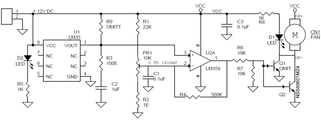
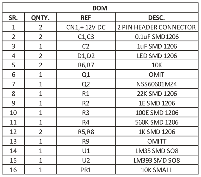
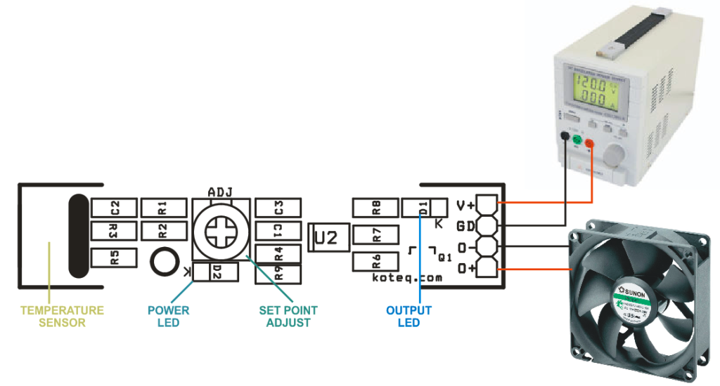
Heat activated cooling fan controller is a simple project which operates a brushless fan when the temperature in a particular area goes above a set point, when temperature return normal, fan automatically turns off. The project is built using LM358 Op-amp and LM35 temperature Sensor. Project requires 12V DC supply and can drive 12V Fan. This project is useful in application like Heat sink temperature controller, PC, heat sensitive equipment, Power supply, Audio Amplifiers, Battery chargers, Oven etc
The SMD SO8 LM35 used as temperature sensor, LM358 act as comparator and provides high output when temperature rise above set point, high output drive the Fan through driver transistor. The LM35 series are precision integrated-circuit temperature devices with an output voltage linearly-proportional to the Centigrade temperature. The LM35 device has an advantage over linear temperature sensors calibrated in Kelvin, as the user is not required to subtract a large constant voltage from the output to obtain convenient Centigrade scaling. The LM35 device does not require any external calibration or trimming to provide typical accuracy of ±¼°C at room temperature. Temperature sensing range 2 to 150 centigrade. LM35 provides output of 10mV/Centigrade.
Electromagnetism is a branch of physics and engineering that includes the study of electric and magnetic fields and their interactions. Electricity and magnetism are two aspects of electromagnetism. This concept describes how electric currents create magnetic fields and how changing magnetic fields induce electric currents. Electromagnetism involves phenomena such as electromagnetic induction, electromagnetic waves (including light), and the behavior of charged particles in electric and magnetic fields.
In physics, electromagnetism is one of the fundamental forces of nature. In engineering, electromagnetism plays a crucial role in various disciplines such as electrical engineering, electronics, telecommunications, and electromechanical systems. Engineers always utilize principles of electromagnetism to design and develop devices like motors, generators, transformers, antennas, and communication systems.
Historically, electricity and magnetism were long thought to be separate forces. It was not until the 19th century that they were finally treated as interrelated phenomena. In 1905 Albert Einstein’s special theory of relativity established that both are aspects of one common phenomenon.
An important aspect of electromagnetism is the science of electricity, which is concerned with the behavior of aggregates of charge, including the distribution of charge within matter and the motion of charge from place to place.
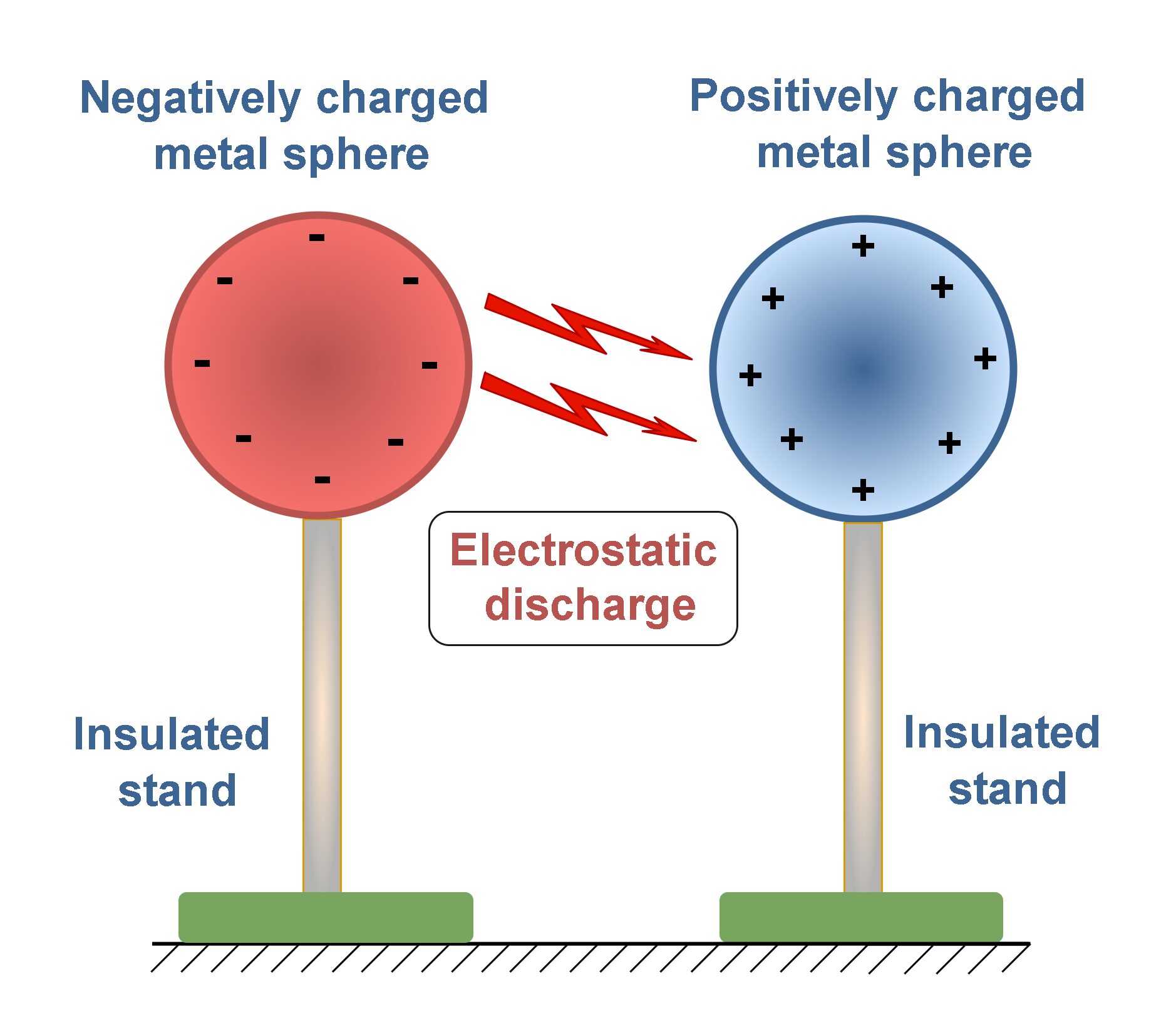
At a microscopic scale, the electric force in particular is responsible for most of the physical and chemical properties of atoms and molecules. It is strongly compared with the force of gravity. At a more familiar macroscopic scale, electric phenomena are responsible for the lightning and thunder accompanying certain storms in nature. Such conditions can be simulated in a laboratory with two oppositely charged metal spheres which are installed on insulated stands. If we bring them close to each other, in a certain distance we may observe some sparks because of electrical discharge between spheres, as Figure 1 shows.
Figure 1: The electrical discharge phenomenon
Electricity is the lifeblood of technological civilization and modern society. Without it, we revert to the mid-nineteenth century: no telephones, no television, none of the household appliances that we take for granted. Instead, with the discovery and harnessing of electric forces and fields, we can view arrangements of atoms, probe the inner workings of the cell, and send spacecraft beyond the limits of the solar system.
Static Electric Charges
Electrostatics is a branch of physics that studies the interaction between slow-moving or stationary electric charges. It focuses on phenomena involving static electricity, where charges are not in motion.
Around 600 B.C. the ancient Greek philosophers conducted the earliest known study of electricity. It all began when Thales noticed that a fossil material called amber would attract small objects after being rubbed with wool because it became electrically charged. Subsequent experiments found that most materials when rubbed possessed this property. We say that they are electrified (a word derived from elektron, the Greek name for amber).
An officer in the French Army Engineers, Colonel Charles Coulomb (1736- 1806), performed an elaborate series of experiments to determine quantitatively the force exerted between two objects, each having a static charge of electricity.
Experiments also demonstrate that there are two kinds of electric charge, which the American scientist Benjamin Franklin (1706- 1790) named positive and negative charges.
A charge is a basic property of matter. Most bulk matter has an equal amount of positive and negative charge and thus has zero net charge.
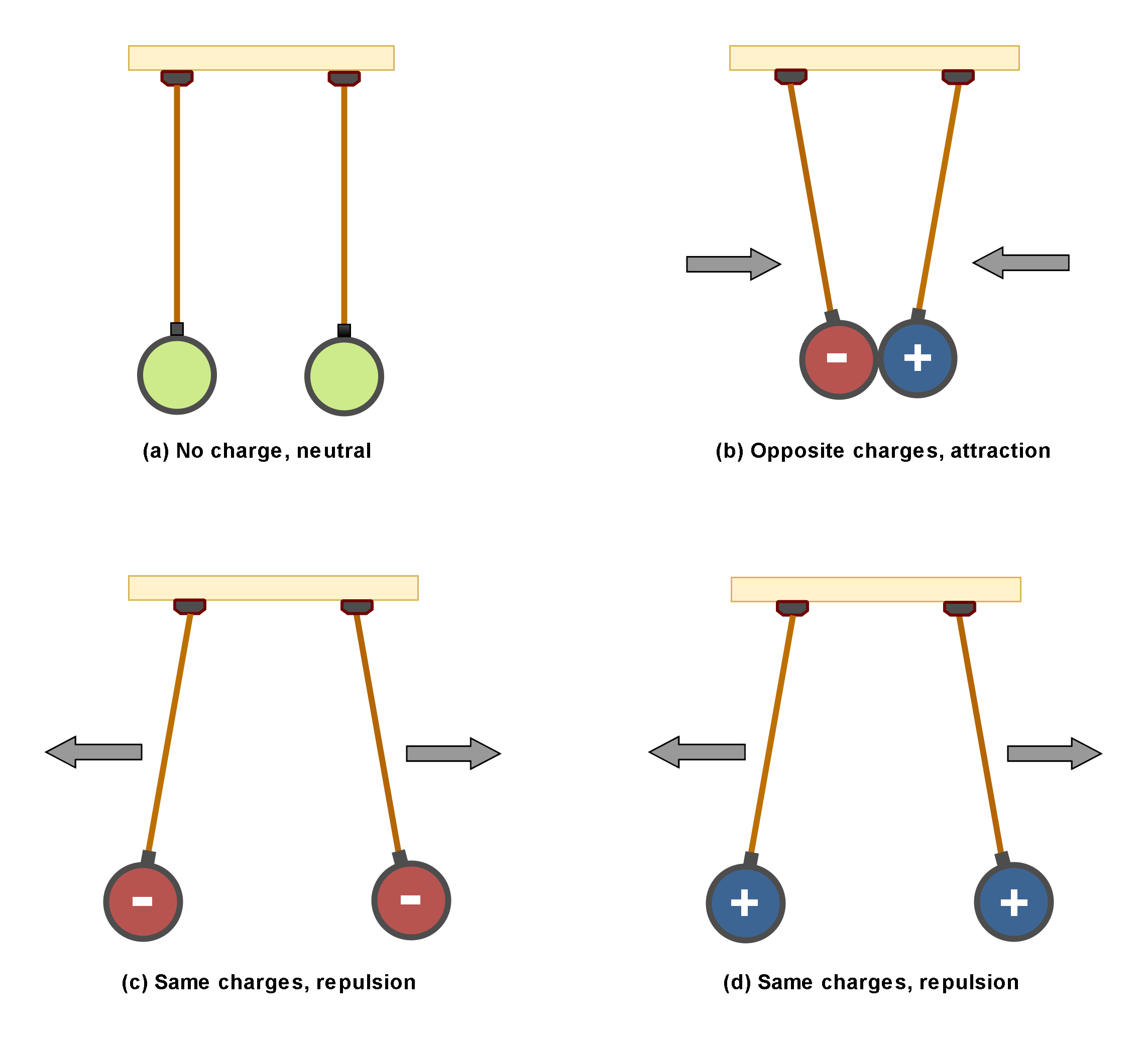
Figure 2 illustrates the interaction of two charges. There are 2 objects (for example 2 metallic spheres) suspended by insulated strings.
Figure 2: The interaction of two charges
In Figure 2(a), both of objects are uncharged and there is not any interaction between them. In Figure 2(b), they are oppositely charged and then there are attraction forces between them. This is one of the main physical principles that charges of opposite signs, attract each other.
In Figure 2(c) and 2(d), the objects are similarly charged and then there are repulsive forces between them. This is another physical fact that charges of the same signs, repel each other.
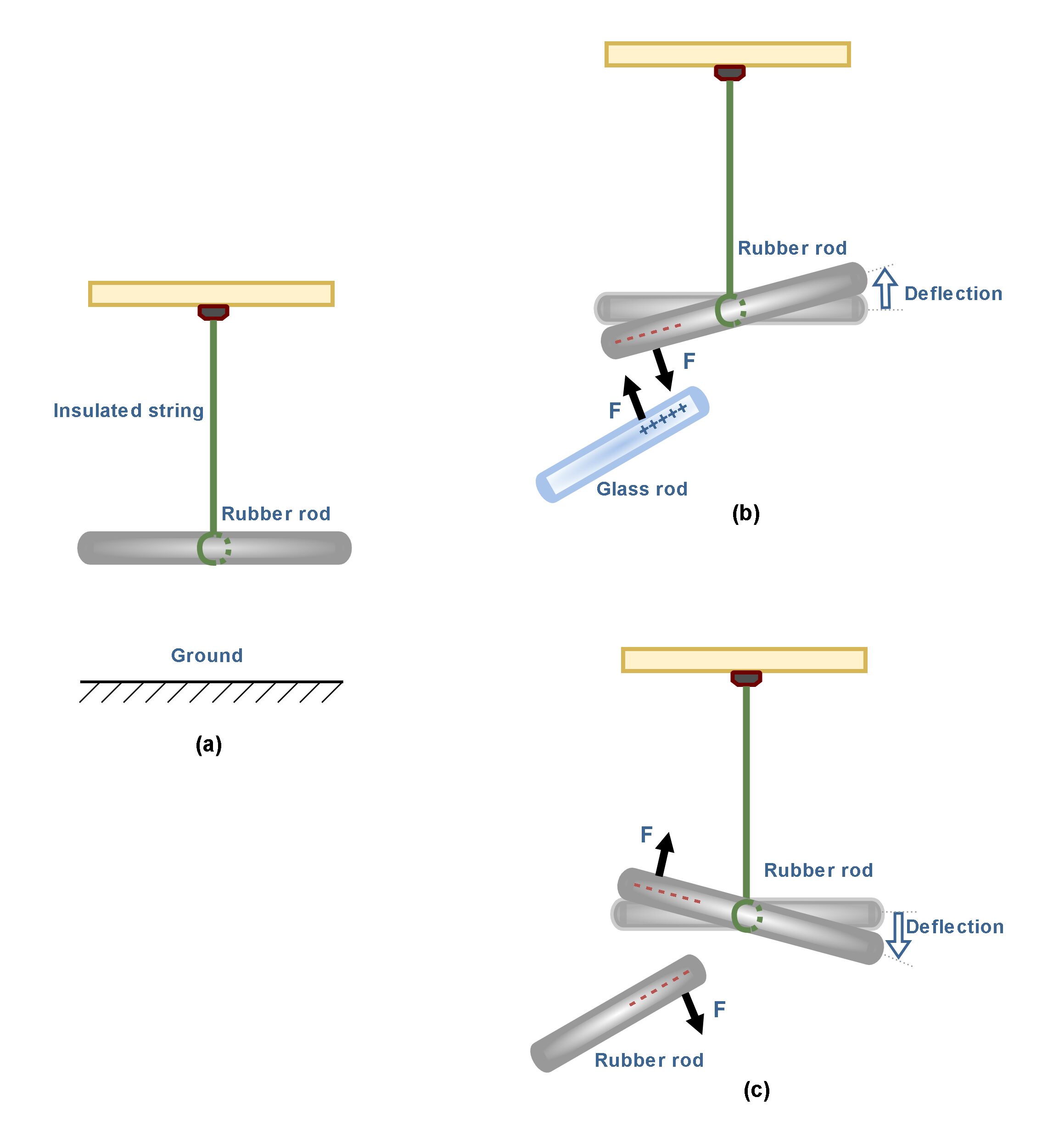
As a more realistic example, Figure 3 shows an experimental setup for observing the electrical force between two charged objects.
Figure 3: An experimental setup for observing the electrical force between two charged objects
In Figure 3(a) there is an uncharged hard rubber rod that is suspended by a piece of insulated string over the ground. We might assume that the rubber rod has already been rubbed with fur before suspending. Then, it has absorbed some negative charges. Also, we have a glass rod which has already been rubbed with silk and then it has lost some negative charges. When the positively charged glass rod is brought near the rubber rod, the rubber rod is attracted toward the glass rod because the electrostatic force between them is attractive as shown in Figure 3(b).
If two charged rubber rods (or two charged glass rods) are brought near each other, as in Figure3(c), the force between them is repulsive. These observations may be explained by assuming the rubber and glass rods have acquired different kinds of charge, where the electric charge on the glass rod is positive and that on the rubber rod is negative.
Atomic Nature Of Electricity
Atoms are the basic particles of the chemical elements. The word atom is derived from the ancient Greek word “atomos”, which means “uncuttable”.
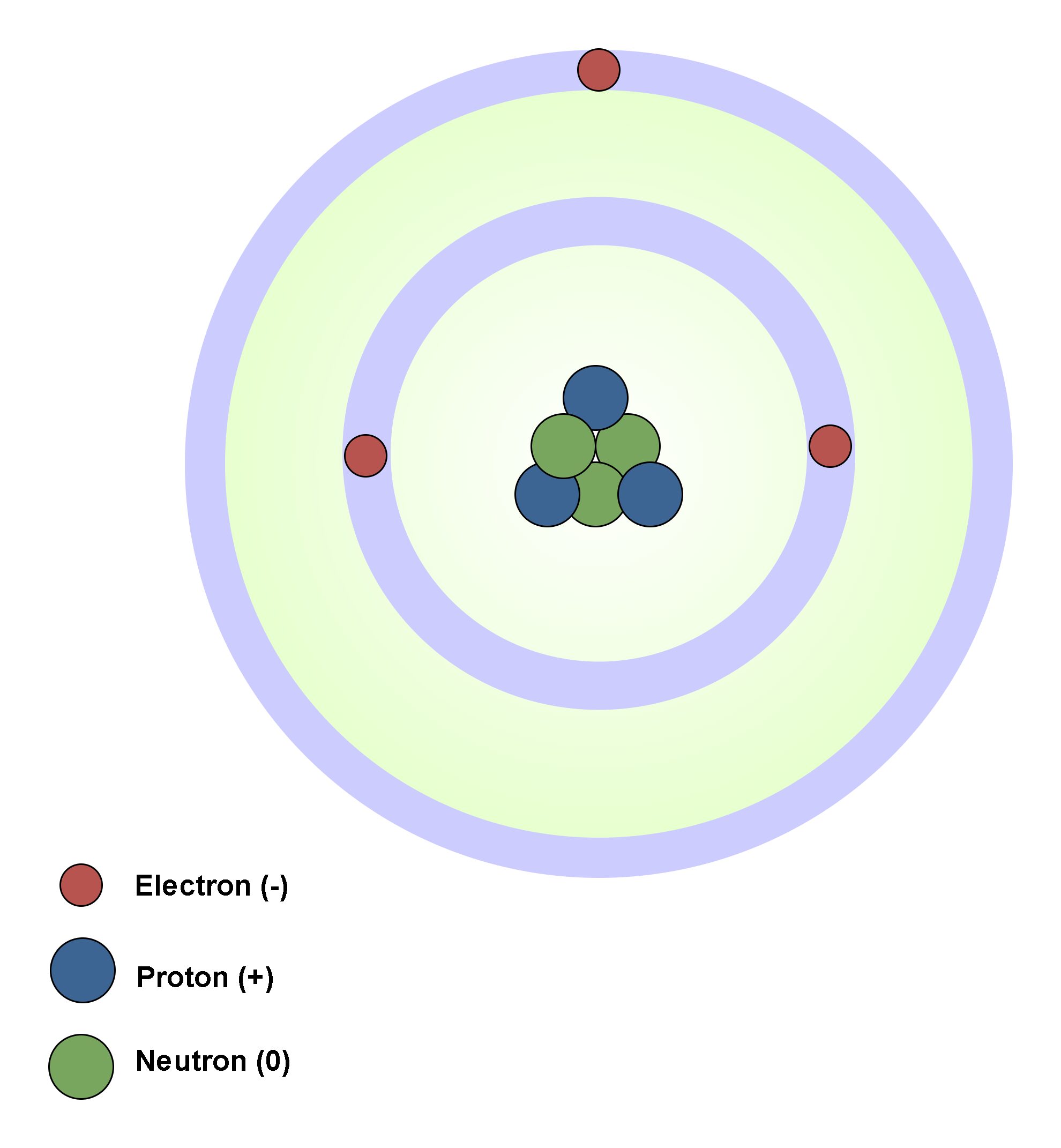
In atomic physics, the Rutherford–Bohr model of the atom, presented by Niels Bohr and Ernest Rutherford in 1913, consists of a small, dense nucleus surrounded by orbiting electrons. It is analogous to the structure of the Solar System, but with attraction provided by electrostatic force rather than gravity, and with the electron energies quantized (assuming only discrete values). Figure 4 shows the simplest classic physical model of an atom.
Figure 4: The classic physical model of an atom
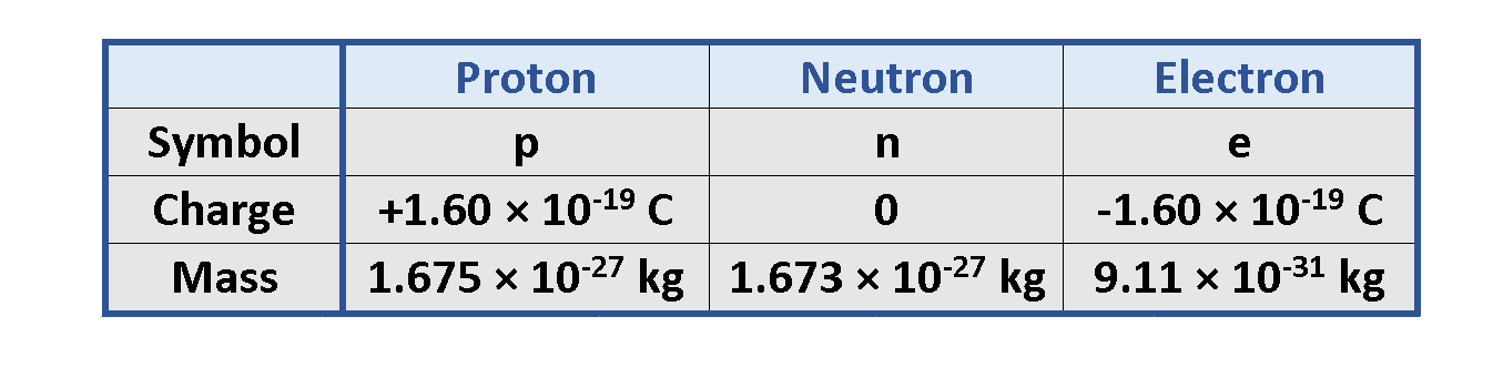
Atom´s nucleus contains practically the whole mass of the atom. It consists of protons and neutrons. Neutrons are not charged. Protons are charged positively and they never move from one material to another. Electrons are small and light negatively charged that rotate around the core in electron shells. They occupy the outer regions of the atom.
In 1909 Robert Millikan (1886–1953) discovered that if an object is charged, its charge is always a multiple of a fundamental unit of charge, designated by the symbol e. Other experiments in Millikan’s time showed that the electron has a charge of -e and the proton has an equal and opposite charge of +e. In modern terms, the charge is said to be quantized, meaning that charge occurs in discrete chunks that can’t be further subdivided.
In the SI (International System of Units) the unit of electric charge is the Coulomb or C. The amount of charge of one proton is qp = +e = 1.60 × 10⁻¹⁹ C.
Table 1 provides information about particles of an atom containing the charge and mass of each component.
Table 1: The basic components of an atom
Electrons are far lighter than protons and hence more easily accelerated by forces. A typical atom contains many electrons that can be closer to or further from the core. Those further from the core are loosely bound and they can be removed by rubbing or other methods. Rubbing the two materials together serves to increase the area of contact, facilitating the transfer process.
Normally atoms are not charged. A neutral atom (an atom with no net charge) contains as many protons as electrons. Removing electrons creates a positively charged ion and placing additional electrons on the atom creates a negatively charged ion. Consequently, objects become charged by gaining or losing electrons.
Essentially, 1C is a very large amount of charge. In typical electrostatic experiments in which a rubber or glass rod is charged by friction, there is a net charge on the order of 10-6 C.
As a tangible example, an ordinary flashlight battery delivers a current that provides a total charge flow of approximately 5,000 Coulombs, which corresponds to more than 1022 electrons, before it is exhausted!
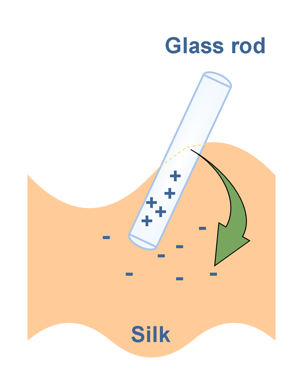
When a glass rod is rubbed with a piece of silk cloth, as in Figure 5, electrons are transferred from the rod to the silk. As a result, the glass rod carries a net positive charge and the silk carries a net negative charge.
Figure 5: Electrifying a glass rod by rubbing it with silk
The transmission of electric charges between objects, due to rubbing them together, is shown in Figure 6. If there are more protons than electrons, the object will be positively charged, and if there are more electrons than protons, it will be negatively charged. In Figure 6 (a) there are two objects without any physical contact and in the neutral state with equal amounts of positive and negative charges. In Figure 6 (b) and (c) there is physical contact between them which causes the transfer of electrons between the objects. Consequently, we have two charged objects (positively and negatively) instead of neutral ones.
Figure 6: Transferring electric charges by physical contact
Insulators And Conductors
Substances can be classified in terms of their ability to conduct electric charge. In conductors, electric charges move freely in response to an electric force. All other materials are called insulators.
Glass and rubber are insulators. When such materials are charged by rubbing, only the rubbed area becomes charged, and there is no tendency for the charge to move into other regions of the material. In contrast, materials such as copper, aluminum, and silver are good conductors. When such materials are charged in some small region, the charge readily distributes itself over the entire surface of the material.
Semiconductors are a third class of materials, and their electrical properties are somewhere between those of insulators and those of conductors. Silicon and germanium are well-known semiconductors that are widely used in the fabrication of a variety of electronic devices.
Coulomb´S Law
In 1785 Charles Coulomb experimentally established the fundamental law of electric force between two stationary charged particles. An electric force has the following properties:
The direction of the electric force is along the line connecting the charges.
The magnitude of the force F is proportional to the product of the magnitudes of the charges, q1 and q2, of the two particles.
The magnitude of the force F is inversely proportional to the square of the separation distance r, between the two charges, q1 and q2.
It is attractive if the charges are of opposite sign and repulsive if the charges have the same sign.
The force depends on the medium in which the charges are placed.
Based on his observations, Coulomb proposed the following mathematical formula for the vector electric force F between two charges q1 and q2 separated by a distance r as explained in Equation 1.
Equation 1: Coulomb’s law
where ke is a constant called the Coulomb constant. The vector electric force F involves both magnitude and direction. In Equation 1 the direction of force is governed by the unit radius vector r12 in the direction from q1 to q2. In the SI system, q1 and q2 are measured in Coulombs (C) and r in meters (m), and the force F should be Newtons (N). The value of the Coulomb constant in Equation1 depends on the choice of units. From the experiment, we know that the Coulomb constant in SI units has the value explained in Equation2.
Equation 2: Coulomb constant
Equation1, known as Coulomb’s law, applies exactly only to distinct point charges and to spherical distributions of charges, in which case r is the distance between the two centers of charges. If the force formula yields a positive value, charges repel each other. If it yields a negative value, the charges attract each other. Electric forces between stationary and unmoving charges are called electrostatic forces.
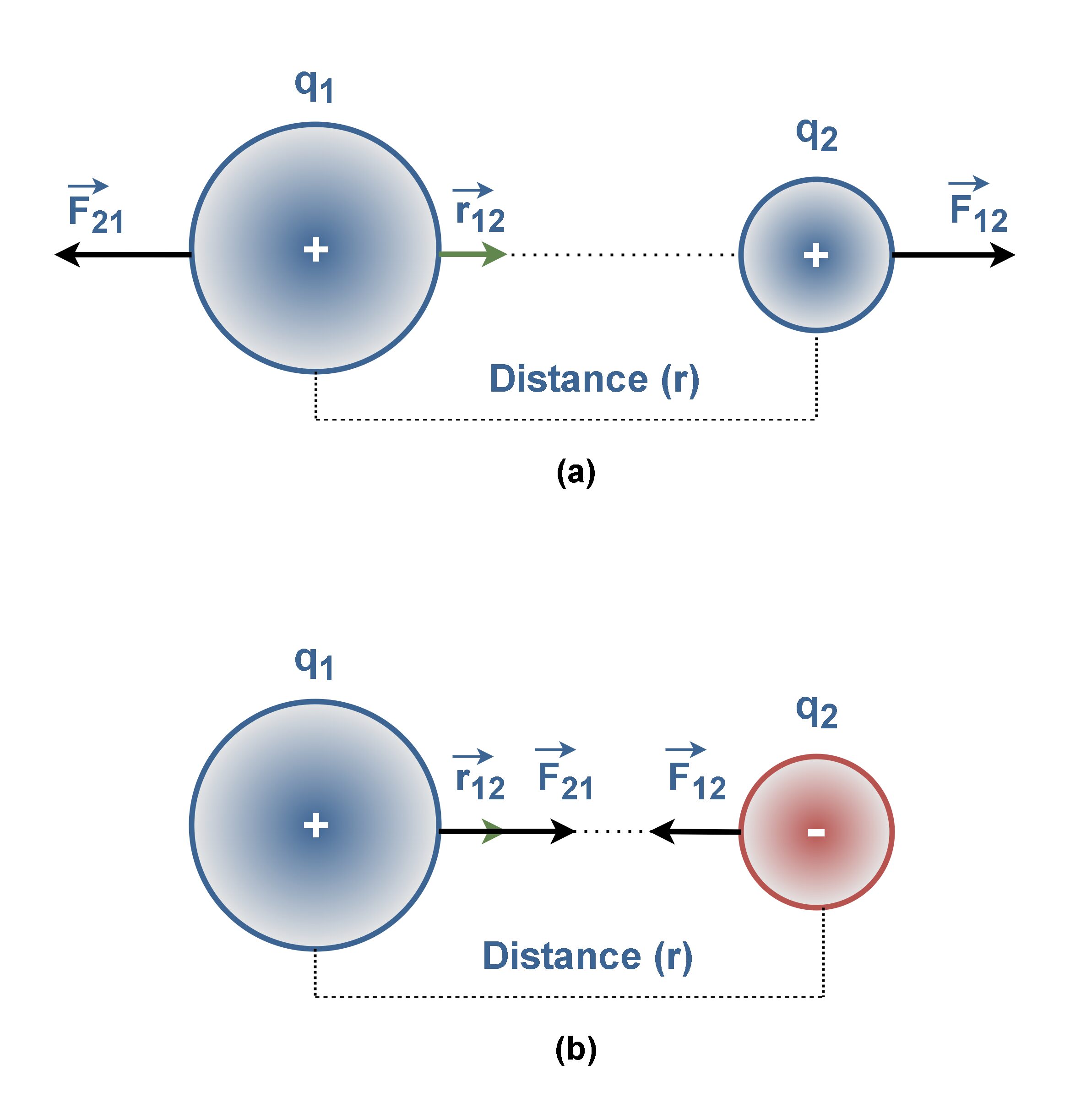
Figure 7: The electric force between two (a) similar, and (b) dissimilar sign charges
Figure 7 shows the exertion of electric forces, F12 (the force exerted by particle 1 on particle 2) and F21(the force exerted by particle 2 on particle 1) between similar-sign and dissimilar-sign q1 and q2 charges.
Figure 7(a) shows the electric force of repulsion between two positively (or two negatively) charged particles. Also Figure 7(b) shows the electric force of attraction between two opposite-sign charged particles.
Like other forces, electric forces obey Newton’s third law. Hence, the forces F12and F21are always equal in magnitude but opposite in direction, regardless of whether q1 and q2 have the same magnitude or not.
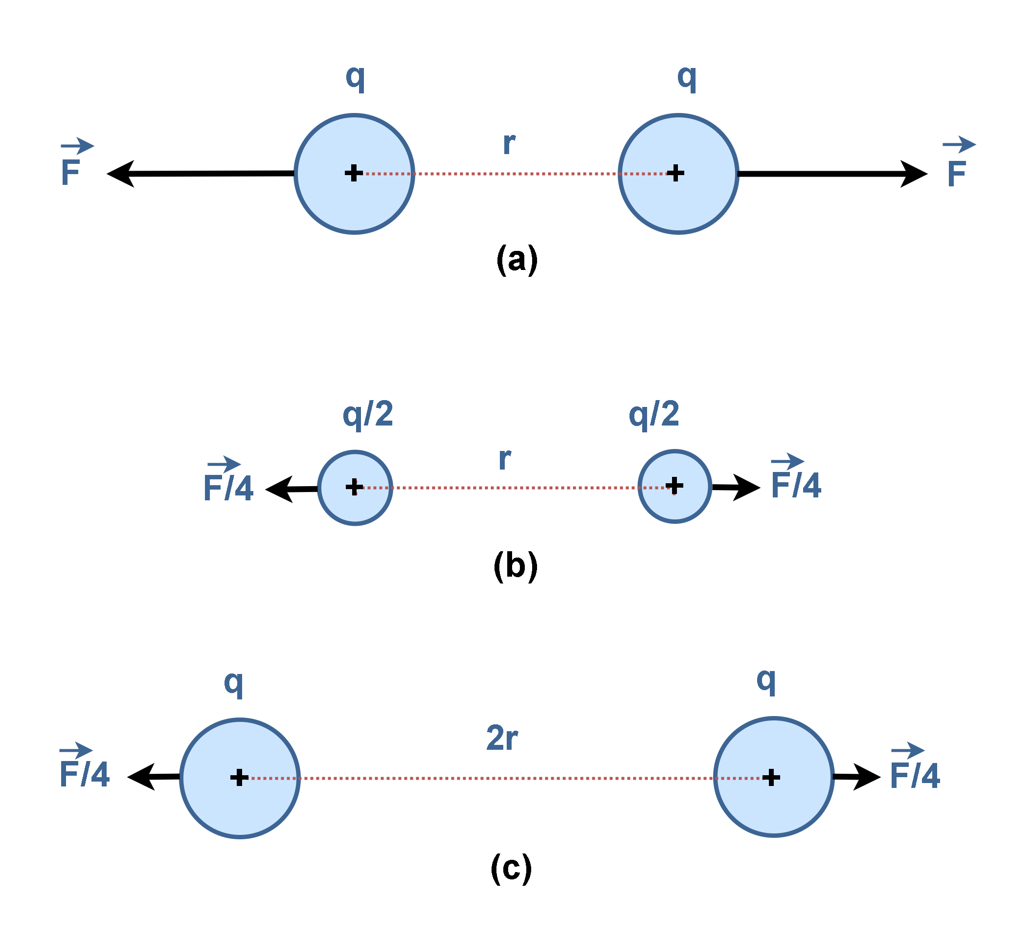
According to Equation1, if there were two positive equal charges, q, they would repel each other with the force that depends on the product (q × q) as illustrated in Figure 8(a). If each of the charges were reduced by one-half, the repulsion would be reduced to one-quarter of its former value, F/4, as depicted in Figure 8(b).
Figure 8: The effects of size and distance between charges on the electric force F
Additionally, if the distance between the two charges is doubled (2 × r), the force becomes weaker, decreasing to one-fourth of the original value (F/4), as depicted in Figure 8(c).
Another expression for the above-mentioned law is related to the definition of the permittivity (ϵ) which is a property of the medium. In the Coulomb’s law, the constant ke can also be written as Equation 3.
Equation 3: Coulomb constant
The new constant ϵ0 is called the permittivity of free space and has magnitude, measured in Farads per meter (F/m). Equation 4 defines this quantity.
Equation 4: Permittivity of free space
Thus, the Coulomb’s force law can be rewritten as Equation 5.
Equation 5: Coulomb’s law in terms of permittivity
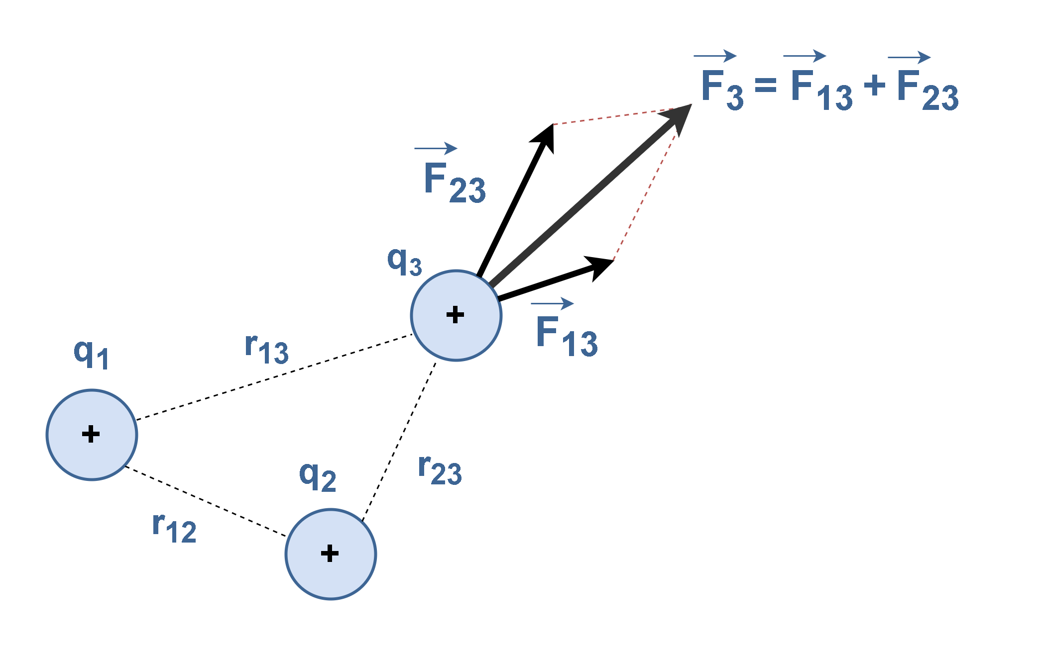
When a number of separate charges act on the charge of interest, each exerts an electric force. These electric forces can all be computed separately, one at a time, and then added as vectors. This is the superposition principle. For example, if there are several charges q1, q2 and q3, the force acting on each charge is the sum of all Coulomb forces acting on the charge from the other charges.
Figure 9 illustrates an example of the final force F3 which is the resultant of the forces exerted on q3 by q1 (F13) and by q2 (F23). Then, F3is the outcome of vector summation of F13 and F23.
Figure 9: The resultant force F3 due to the sum of forces of charges q1 and q2 on q3
Summary
Electromagnetism is the science of electric charge and of the forces and fields associated with the charge.
Electric forces are produced by electric charges either static or in motion.
Electrostatics describes electric charges at rest.
Nature’s basic carriers of positive charge are protons, which, along with neutrons, are located in the nucleus of atoms. Some particles, such as a neutrons, have no net charge.
Then, the smallest subdivision of the amount of charge that a particle can have is the charge of one proton.
The electron has a charge of the same magnitude but the opposite sign of protons.
Normally atoms are neutral as the charge of their electrons balances the charge of their core.
Electrons with negative charges can transfer readily from one type of material to another due to rubbing.
Objects usually contain equal amounts of positive and negative charge, so they are neutral. Electrical forces between objects arise when those objects have net negative or positive charges.
Like charges repel one another and unlike charges attract one another.
Different types of materials are classified as either conductors or insulators on the basis of whether charges can move freely through their constituent matter.
The SI unit of charge is the coulomb (C).
Only a very small fraction of the total available charge is transferred between the rod and the rubbing material.
When using Coulomb’s force law, remember that force F is a vector quantity and must be treated accordingly.
There are three conditions to be fulfilled for the validity of Coulomb’s law: The charges must have a spherically symmetric distribution, the charges must not overlap, the charges must be stationary.
The name “Synchronous Counter” comes from the fact that all the flip-flops inside the counter are driven through a single clock source and because of this parallel clock sourcing arrangement of flip-flops in a synchronous counter, they are often referred to as “Parallel Counters”. This indicates that with each clock pulse, the counter’s output varies concurrently and reliably. In addition to having shorter propagation latency and power usage than asynchronous counters, synchronous counters are simpler to build and evaluate. Nevertheless, they also need more wires and logic gates, which raises the circuit’s potential cost and complexity.
Synchronous counters can be built with Toggle or D-type flip-flops. In contrast to asynchronous counters, which have a direct connection between the output of the preceding stage and the clock input of the next counter stage in the chain, the synchronous counter has synchronized timing for each level. Therefore, the overall operation is faster in synchronous counters compared to asynchronous ones.
The issue with asynchronous counters is that they experience a phenomenon called “Propagation Delay,” whereby the timing signal has a slight delay as it passes through each flip-flop. On the other hand, the external clock signal is connected to the clock input of each flip-flop within the synchronous counter. This results in all the flip-flops being synchronously timed (in parallel) with each other, providing a fixed time correlation. Stated differently, the output is “synchronized” with the clock signal as it varies.
As a result of this synchronization, there is no propagation delay since every single output bit changes its state in response to the common clock signal at precisely the same moment.
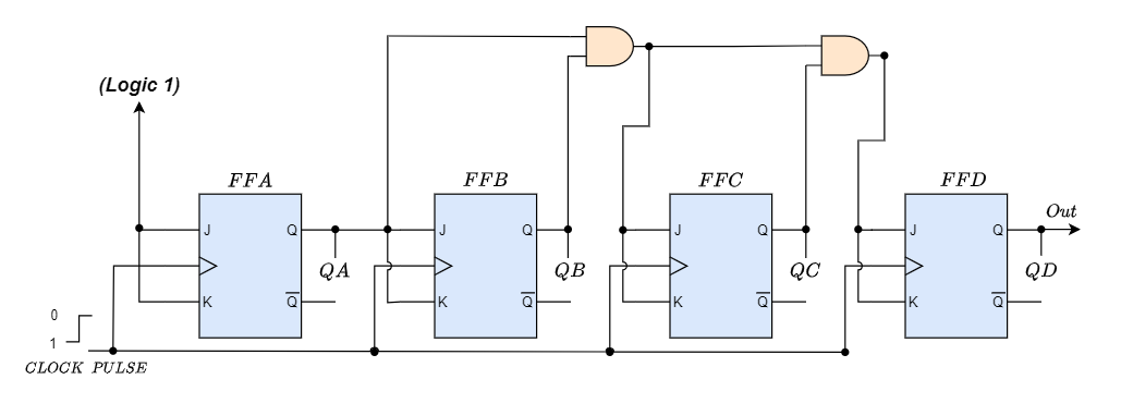
Binary 4-bit Synchronous Up Counter
Fig-1: 4-bit Synchronous Up Counter
As shown in the picture above, the JK flip-flops in the counter chain are fed by the same external clock pulses, which are meant to be counted. The J and K inputs are connected in toggle mode, but only the flip-flop FFA (LSB), which is the first flip-flop, has HIGH logic (1) connected to it, allowing it to toggle on every clock pulse. Afterward, in reaction to the common clock signal, the synchronous counter advances one state for every pulse in a predefined sequence.
The J and K inputs of flip-flop FFB are directly linked to the output “QA” of flip-flop FFA, while the J and K inputs of flip-flops FFC and FFD are driven by independent AND gates that are additionally provided with signals from the input and output of the preceding stage. The necessary logic for the JK inputs of the subsequent level is produced by these extra AND gates.
The same counting sequence as with the asynchronous circuit may be obtained if we enable each JK flip-flop to toggle depending on whether all previous flip-flops’ outputs (Q) are “HIGH.” This eliminates the ripple effect because every flip-flop in this circuit will be timed at precisely the same time.
Since all the counter stages are triggered simultaneously in parallel, synchronous counters do not have an intrinsic propagation delay, hence their maximum operating frequency is significantly higher than that of an equivalent asynchronous counter circuit.
4-bit Synchronous Counter Waveform Timing Diagram
Fig-2: Synchronous Counter Timing Diagram
The outputs of this 4-bit synchronous counter count upward from 0 (0000) to 15 (1111) because it counts consecutively on each clock pulse. As such, such kind of counter is also termed as a 4-bit Synchronous Up Counter.
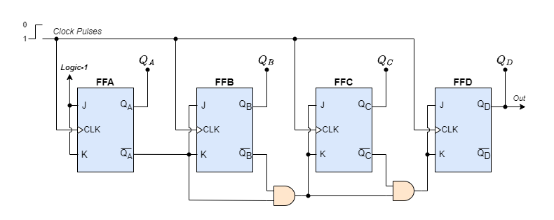
On the other hand, by connecting the AND gates to the flip-flops’ Q̅ output as demonstrated, we can quickly build a 4-bit Synchronous Down Counter and create a timing diagram that is the opposite of the one above. In this case, the counter begins with all its outputs HIGH (1111) and counts down to zero (0000) with each clock pulse application before repeating the sequence.
Binary 4-bit Synchronous Down Counter
Fig-3: 4-Bit Synchronous Down Counter
Since synchronous counters are made by joining flip-flops together, any number of flip-flops can be joined or “cascaded” together to create a binary counter that is “divide-by-n.” The modulo, or “MOD,” number remains the same as it does for asynchronous counters, allowing truncated sequences to be built alongside a Decade counter or BCD counter that has counts ranging from 0 to 2n-1. Adding an extra flip-flop and AND-gate across up or down the synchronous counter is required to enhance its MOD count.
4-bit Synchronous Decade Counter
Synchronous binary counters may also be used to construct a 4-bit decade synchronous counter, which will provide a count sequence from 0 to 9. With the help of extra circuitry, a regular binary counter may be transformed into a decade (decimal 10) counter to achieve the necessary state sequence. The counter resets to “0000” whenever it reaches the number “1001”. We now have a Modulo-10 counter or decade.
Fig-4: 4-Bit Synchronous Decade Counter
When the counting sequence hits “1001” (Binary 9), which is detected by the extra AND gates, flip-flop FF3 toggles on the subsequent clock pulse. Flip-flop (FF0) toggles on and off with each clock pulse. As a result, the count restarts at”0000,” creating a synchronous decade counter.
The extra AND gates in the counter circuit above can be readily rearranged to generate other count numbers. For example, a Mod-12 counter counts 12 states from “0000” to “1011” (0 to 11) and then repeats, making it appropriate for clocks and other applications.
Triggering The Counter
Synchronous counters employ edge-triggered flip-flops, which produce a single count when the clock input switches states on either the “positive edge” (rising edge) or the “negative edge” (falling edge) of the clock pulse on the control input.
Synchronous counters typically count on the rising edge of the clock signal, which is the transition from low to high, whereas asynchronous ripple counters count on the falling edge, which is the transition from high to low.
Fig-5: Counter State Change
The most significant bit (MSB) of one counter can control the clock input of the next stage flip-flop, which makes it easier to link counters together even if it may seem strange since ripple counters utilize the clock cycle’s “falling edge” to change states.
This can function because a carry to the next bit must happen at the time when the preceding bit goes from high to low. To connect counters without causing any propagation delays, synchronous counters often have a carry-out and a carry-in pin.
Applications of Synchronous Counters
Digital circuits used in embedded systems, automotive systems, and consumer electronics are all built with synchronous counters. They have precise timekeeping capabilities and drive time displays in forms like hours, minutes, and seconds.
In Arithmetic Logic Units (ALUs), synchronous counters are employed to carry out addition, subtraction, multiplication, and division operations on binary integers. In computation-intensive applications and digital signal processing, they help to efficiently implement digital arithmetic algorithms.
In digital systems, synchronous counters are essentially required for producing accurate timing signals and managing the order of processes. They are utilized in timing generators to produce clock signals with precise frequencies and duty cycles, as well as in synchronization circuits to guarantee synchronized activities among various system components.
They are useful in industrial automation operations, where synchronous counters are used in situations where precise counting of events or occurrences is required. This might include keeping track of the frequency of transmissions in communication systems or counting the pulses in sensor systems.
Advantages:
The Synchronous counter operates faster as they are not accompanying any propagation delay.
Error probabilities decreased because logic gates regulate the count sequence.
synchronous counters are more suitable for high-speed and accurate operations, such as frequency division, binary arithmetic, and digital clocks.
Synchronous counters can easily be modified and extended to create different types of counters, such as up-down, modulo-n, and ring counters.
Disadvantages:
The circuit gets increasingly complex as the number of states rises.
An asynchronous counter has a single common clock pulse that drives all its flip-flops.
When compared to asynchronous counters, they require more hardware and components.
Synchronous counters can consume more power than asynchronous counters since they have more logic gates and wiring that draw current.
Conclusion
Synchronous counters operate using a single clock signal to drive all flip-flops within the counter, simultaneously. This ensures that all the outputs are synchronized with the clock signal, eliminating propagation delays present in asynchronous counters.
D-type or Toggle flip-flops can be used to create synchronous counters.
Synchronous counters can be used for the construction of modular counters, including decade counters that count from 0 to 9. These counters reset after reaching the maximum count, achieved through additional circuitry.
Logic gates are used to regulate the count sequence.
Compared to asynchronous counters, synchronous counters are simpler to construct.
It is possible to get an overall speedier operation as compared to asynchronous counters.
Synchronous counters are more suitable for high-speed and accurate operations, such as frequency division, binary arithmetic, and digital clocks.
So you’ve just finished designing your new PCB, completed all ERC and DRC checks, and sent the files off to the manufacturer. Now, you’re eagerly awaiting the arrival of your new PCBs. If you’re like me, once you’ve generated your Gerber files, you head to an online Gerber viewer site like PCBWay or JLCPCB to inspect your PCBs for any additional aesthetic errors and then send them off to your manufacturers.
But what if I tell you there’s a better way to check your Gerber files which will give you various additional analysis tools to get those sneaky errors out of your design? That’s where NextPCB’s Free Gerber Viewer (HQDFM) comes in. Gerber files are the standard in PCB design, containing crucial data for manufacturers. Analyzing them can be complex, but HQDFM’s software simplifies the process, offering a user-friendly interface and resources, designers can ensure manufacturability and spot errors efficiently.
What Does DFM Stand for and Why It’s Important?
DFM stands for “Design for Manufacturability” or “Design for Manufacturing.” It’s an engineering approach that focuses on designing products in a way that makes them easier and more efficient to manufacture. DFM aims to streamline the manufacturing process, reduce costs, improve quality, and shorten time to market by considering manufacturing constraints and requirements during the design phase.
In a practical term we check for Tracewidth/spacing, Drill hole/slot sizes, Clearances to copper and board, Layer to Layer drill holes, solder mask openings, silk screen errors, and more.
What is HQDFM and What is so Special About it?
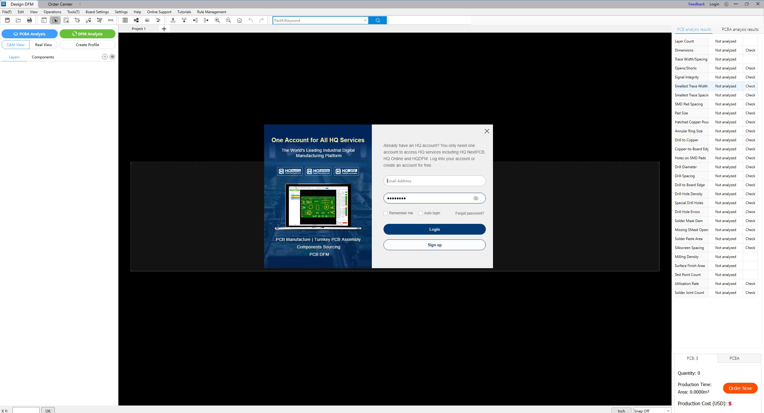
HQDFM is NextPCB’s Free Gerber Viewer tool It is a powerful and user-friendly tool that supports Gerber X2, RS-274X, and ODB++ file formats. With zoom, pan, and measurement tools, ensure quality and integrity in your PCB designs. Seamlessly compatible with Altium, Eagle, and KiCad, it offers advanced features like layer selection and transparency control for detailed analysis. Once you download the tool you need to create your own free account and log in to work with this tool.
The tool is easy to use, once installed just drag and drop the Gerber and it gets uploaded to the software, it also features a One-click PCB file checker for quick analysis and generates a report through which you can analyze the PCB. On top of that penalization, impedance calculator, routing distance calculator, and more features make the diagnosis process easier. It can also generate BOM and coordinate files to order the PCB from the next website. The tool is completely free and can be used by anyone.
How to Use the HQDFM Tool
To begin using the Design for Manufacturability (DFM) tool, import your Gerber file, and you also need to import your BOM file if you are willing to check a new window will open for that. Now click on the “DFM Analysis” A detailed analysis of your PCB will start presenting results for PCB and PCBA analyses. Now you can correct any design errors based on these results to prevent real-life issues. You will get an estimated price of 5 quantities of your PCB and expected making time.
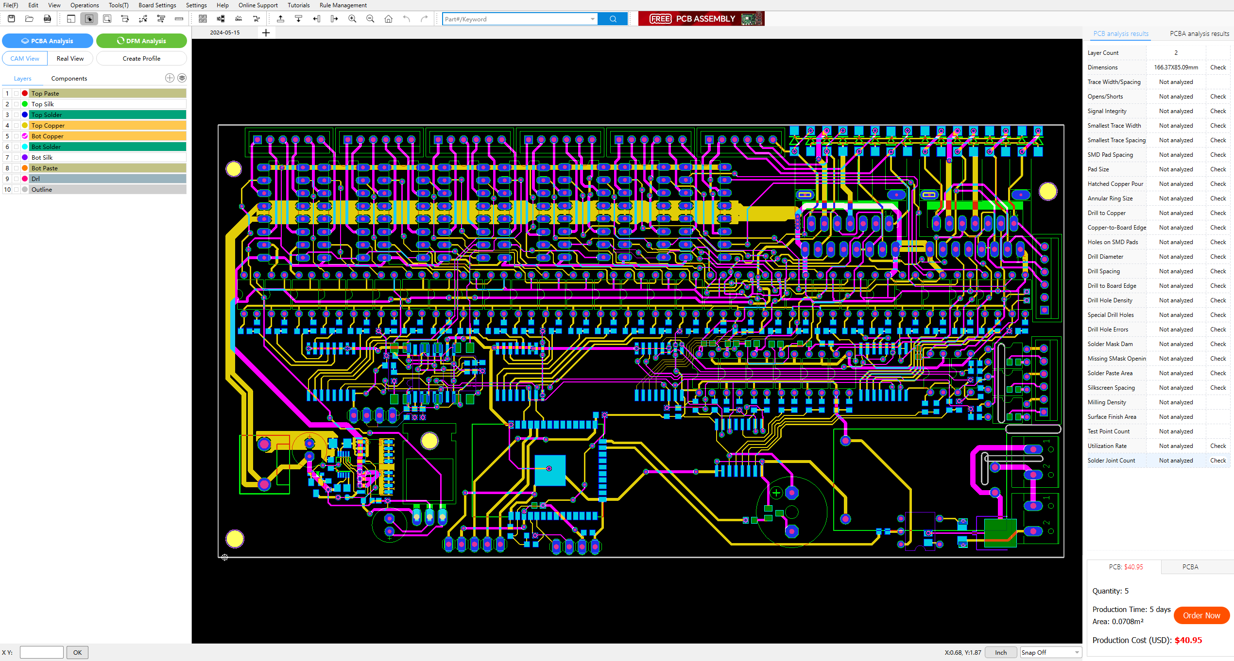
All Layer View in HQDFM
The DFM analysis section offers CAM view, Real View, and profile creation as an added option. It includes layer and component lists for PCB inspection. The tools section in the menu bar provides additional features like an impedance calculator, file comparison, copper area calculation, and more.
BOM and centroid file checker
One of the most powerful features of this tool is the BOM and centroid file checker, the HQDFM identifies inconsistencies in BOM and Centroid files, which are hard to detect manually and can lead to confusion during assembly. It checks for quantity mismatches, duplicate entries, and incorrect part values, saving engineers from tedious manual review tasks. HQDFM also checks whether all the parts in the BOM are present in the centroid data system, which may be a result of poor version control setup.
Footprint Checker
The new update includes a powerful footprint checker that compares PCB design land patterns with the expanding HQDFM database. With a single click, it checks over half of the BOM parts and offers immediate feedback on problematic patterns. There is also the option for the Users can expand the database or manage a local one.
DFA analysis
DFA Found Misplaced VIA on the PCB
HQDFM’s DFA checks utilize component and x-y coordinate data to simulate accurate component placement, even without existing footprint data. It includes checks for pad size, hole diameter and placement, component clearances, pad contact areas, and PCB shadowing. Based on IPC guidelines and real assembly data, HQDFM’s generic feedback benefits all PCB layout engineers by focusing on general industry capabilities rather than specific assembler processes.
The new HQDFM additions offer significant verification checks for PCB design, addressing commonly encountered assembly problems. This free software educates designers and provides early resolution tools. Download the updated HQDFM suite from the official HQ Electronics (NextPCB) website. A free online Gerber Viewer version is also available for new users or non-Windows users needing bare PCB DFM features.
You may also find interesting (Promo offers):
Free assembly for 5 pieces PCBA: For free PCB assembly, no coupon code or application is required. Just go to the PCB assembly order page and follow the step-by-step instructions. If your order fulfills the free assembly conditions, the assembly, setup and operation fees will automatically be deducted on the spot and you only pay for the PCB, components and shipping. The free assembly offer can be used multiple times.
50% off Batch PCB Assembly from HQ NextPCB: All users who log into their HQ Electronics account will receive a 50% off PCB assembly coupon. To use it, add the qualifying order to your shopping basket and select the coupon at the checkout. The coupon can only be used once (The coupon can be found in your account after logging in).
NextPCB offers the best value for money in the market with rich capabilities, quality, speed, and customer service. Whether you are developing a new product or a one-off project, there is no excuse not to give us a try. Visit the PCBA order page or try the links below to get started.
RF-star, a leading manufacturer of wireless modules and provider of wireless connectivity solutions, proudly announces the expansion of its Bluetooth module lineup tailored specifically for automotive applications. The latest BLE modules include the RF-BM-2642QB1I and RF-BM-2340QB1, designed to excel in automobile-critical applications such as digital car keys, T-Box, Tire Pressure Monitoring Systems (TPMS), Passive Entry Passive Start (PEPS), and more.
Designed to meet the evolving demands of the automotive industry, RF-star’s new modules offer a host of features to enhance reliability, durability, security, and ease of integration.
Compliance and security assurance are paramount in automotive applications
RF-star’s new Bluetooth Low Energy modules are based on TI chips, specifically the CC2642R-Q1 and CC2340R5-Q1 MCUs meeting Automotive Electronics Council (AEC-Q100) standards. RF-BM-2642QB1I and RF-BM-2340QB1 BLE modules integrated with the automotive-qualified MCUs can operate in Grade 2 temperature range (–40 °C to +105 °C), guaranteeing their reliability and durability in harsh automotive environments.
Additionally, RF-star’s CC2642R-Q1 and CC2340R5-Q1 modules incorporate AES 128-and 256-bit cryptographic accelerator, ECC and RSA public key hardware accelerator and true random number generator(TRNG). These advanced security enablers with robust encryption protocols and authentication mechanisms, provide peace of mind to both automakers and end-users.
Rich resources and ease of use are also taken into consideration by project decision-makers
Their high-performance processor and abundant resources, eg., RF-BM-2340QB1 with 512 kB Flash and 36 kB RAM, offer ample opportunities for firmware development. Meanwhile, they also support over-the-air upgrade (OTA).
Besides, the automotive modules feature UART, SPI, I2C, I2S, ADC and more digital peripherals, flexible RF output modes(eg., PCB antenna, IPEX connector and half-hole ANT RF pin), and user-friendly development kits. Hence, it is quite easy to integrate into existing vehicle architectures, especially the auto aftermarket applications.
Best of all, both support Bluetooth 5.0 Low Energy serial port transmission for master-slave wireless connections. These rich functions with AT commands streamline the integration process, reducing complexity and accelerating time-to-market for automotive projects. Whether experienced engineers or newcomers to wireless connectivity, they can leverage RF-star’s Bluetooth modules easily to unlock their full potential in ongoing projects.
RF-star – A powerful supplier with abundant experience stands out among competitors
Certified with ISO9001 and IATF16949 (automotive sector quality management systems), the enterprise and the manufacturer meticulously adhere to international quality management standards. RF-star is also honored as a member of the Car Connectivity Consortium (CCC) and Intelligent Car Connectivity Industry Ecosystem Alliance (ICCE).
Beyond indispensable compliance, RF-star has an innovative and professional development team. With over a decade of hands-on experience in manufacturing wireless modules, RF-star earns a high reputation from domestic and overseas customers based on the supply capacity of KK-level OEMs, reliable quality and expert service.
“We are thrilled to introduce our latest BLE modules tailored for automotive applications,” said King Kang, CEO of RF-star. “With the CC2642R-Q1 and CC2340R5-Q1 modules, we aim to empower automakers with robust, secure, and easy-to-integrate solutions that enhance connectivity and user experience in modern vehicles.”
RF-star’s RF-BM-2642QB1I and RF-BM-2340QB1 Bluetooth modules are in stock and ready for immediate shipment. For more information about the automotive BLE modules, please visit www.rfstariot.com.
Rohde & Schwarz extends its portfolio with a 2U high oscilloscope/digitizer tailored for rack mount and other applications where a low-profile form factor is critical. The new MXO 5C series is the company’s first oscilloscope without an integrated display. It delivers the same peformance as the previously introduced MXO 5 series, but with a fourth of the vertical height.
Rohde & Schwarz introduces the new MXO 5C oscilloscope with four or eight channels. The new series is based on the next-generation MXO 5 oscilloscope and specifically addresses rack mount and automated test system applications where users are often confronted with space limitations. The instrument’s 2U vertical height – just 3.5” or 8.9 cm – allows engineers to deploy it in test systems where a traditional oscilloscope with a large display would not fit. The compact form factor is also of value in applications with high channel density where users need a large number of channels in a small volume. Users operate the instrument via the integrated web interface, or they interact with it exclusively programmatically and use the instrument as a high-speed digitizer.
Like other MXO oscilloscopes, the new MXO 5C series builds on next-generation MXO-EP processing ASIC technology developed by Rohde & Schwarz. It offers the fastest acquisition capture rate in the world of up to 4.5 million acquisitions per second. This makes it the world’s first compact oscilloscope that allows engineers to capture up to 99% real-time signal activity enabling them to see more signal details and infrequent events better than with any other oscilloscope.
Philip Diegmann, Vice President Oscilloscopes at Rohde & Schwarz, said:
“While oscilloscopes with large displays work well for bench usage, we’ve had a number of customers ask for a version that is tailored for rack mount applications. At the same time, we have customers who need a large channel count, for example in physics. With the MXO 5C we created a unique instrument that offers the best possible performance for both scenarios.”
The new form factor allows to place many channels in close proximity. The eight-channel model of the MXO 5C provides a channel density of 1500 cm3 per channel and consumes just 23 watts per channel.
While primarily designed for rack mount usage, the instrument doubles as a stand-alone bench oscilloscope. Users can simply attach an external display via the built-in DisplayPort and HDMI connectors, or they can access the instrument’s GUI via a web interface by typing in the oscilloscope’s IP address into their browser. As the first oscilloscope to offer E-ink display technology, the MXO 5C shows the IP address and other critical information on a small non-volatile display on the front of instrument, which stays visible even when power is switched off.
Like the MXO 5, the MXO 5C series comes in both four and eight channel models, in bandwidth ranges with100 MHz, 200 MHz, 350 MHz, 500 MHz, 1 GHz, and 2 GHz models. The starting price of EUR 18 000 for the eight-channel models sets a new industry standard. Various upgrade options are available to users with demanding application needs, such as 16 digital channels with a mixed-signal oscilloscope (MSO) option, an integrated dual-channel 100 MHz arbitrary generator, protocol decode and triggering options for industry-standard buses and a frequency response analyzer to enhance the capabilities of the instrument.
The new MXO 5C series oscilloscopes are now available from Rohde & Schwarz and selected distribution channel partners. For more information on the instrument, visit : https://www.rohde-schwarz.com/product/MXO5C
The SoM helps you leverage the multi-core architecture of the NXP i.MX 95 applications processor family, offering high-speed data processing alongside secure, real-time, and low-power modes. The SoM offers high-speed connectivity options such as 10GbE, USB 3, PCIe® Gen 3, together with Wi-Fi 6 and Bluetooth 5.3 wireless connectivity. The System on Module caters to a wide range of products and applications ranging from automotive connectivity and infotainment systems to Industry 4.0 applications.
The flex domains on the NXP i.MX 95 SoC allows engineers to mix which pieces of IP they want to use in a particular domain. The Multimedia block includes an Arm Mali 3D GPU core, but also an independent 2D GPU with a real-time blend engine. The i.MX 95 SoC is also NXP’s first applications processor to support LPDDR5 DRAM, enabling increased bandwidth for applications leveraging the embedded workload accelerators
Key features of iW-RainboW-G61M:
NXP i.MX 95 applications processor
6 x Cortex-A55 @ up to 2GHz
1 x M33 core @333MHz
1 x M7 core @800MHz
eIQ® Neutron NPU up to 2.0 TOPS
16GB LPDDR5
16Mb QSPI Flash and
16GB eMMC Flash
Wi-Fi 6 & BT 5.3 Connectivity
2x LVDS, 1x MIPI CSI, 1x HDMI
2x Gigabit Ethernet, 2x PCIe 3.0
4x USB 2.0 Host, 1x USB 3.0 OTG
1x SerDes (10G), 2x CAN, 3x I2C, 1x SD (4bit)
SMARC v2.1.1 Standard (82mm x 50mm)
Linux 6.6 BSP Support
MX 95 SAMRC PR image
The SoM is available in Industrial Grade with the associated BSP support and regular software updates from iWave. iWave assures customers a SoM product longevity of 15+ years and complementary ODM models on hardware customization, software customization, and mechanical and thermal analysis.
“iWave is excited to launch the iW-RainboW-G61M System on Module in Embedded World 2024, offering designers a powerful SoC with advanced 3D graphics, neural processing, and a new flex domain architecture, “said Immanuel Rathinam, Vice President – System on Modules at iWave. As a premier partner with early access to NXP technology, iWave iW-RainboW-G61M System on Module, powered by the NXP i.MX 95 applications processor, enables customers to leverage the powerful features of the latest SoC from NXP.”
“The NXP i.MX 95 is designed to deliver the next generation of edge computing performance for the industrial IoT market;” stated Robert Thompson, Director, Secure Connected Edge ecosystem, NXP. “iWave has a long history of developing advanced system on modules based on NXP’s i.MX applications processors. The iW-RainboW-G61M not only extends this collaboration but delivers the features of the i.MX 95 in a module that will accelerate time to market for customers.”
Complementing our System on Module, iWave enables customers with NXP i.MX 95 SoM evaluation kits with the latest software packages to expedite their evaluation and time to market.
Evaluation Kit Features:
2x Gigabit Ethernet Jack
1x PCIe port & M.2 KEY B PCIe
2x USB 2.0 Host Type-A, 1x USB 2.0 OTG Type microAB
USB 3.0 Host Type-A/ Type-C OTG
1x Standard SD
HDMI-Type A Connector
20pin LVDS Connector
MIPI CSI Camera Connector
2x Audio In & Out Jack through I2S Codec
2x CAN Header
MX 95 SAMRC Development kit image
Click here for more details on the NXP i.MX 95-based System on Module and Evaluation Kit.
MYIR has launched a new embedded System on Module (SoM), the MYC-LMX9X, based on the NXP i.MX 9352 processor. This processor belongs to the high-performance i.MX 93 family, featuring dual ARM Cortex-A55 cores clocked at up to 1.7GHz and Cortex-M33 cores running at 250MHz. It also incorporates a 0.5 TOPS Neural Processing Unit (NPU), enabling cost-effective and lightweight AI applications.
i.MX93 Processor Block Diagram
The MYC-LMX9X has a compact size, measuring merely 37mm by 39mm. In addition to the powerful i.MX 9352 CPU, it offers1GB/2GB LPDDR4 RAM, 8GB eMMCstorage, 32KB EEPROM, and a Power Management IC(PMIC), providing a robust foundation for your next embedded design. Leveraging the full capabilities of the i.MX 9352 SoC, the MYC-LMX9X supports a rich set of peripherals, including 2x USB 2.0, 3x SD/SDIO 3.01, 2x Gigabit Ethernet, 2x CAN-FD interfaces, as well as MIPI-DSI, LVDS and RGB display interfaces, and MIPI-CSI and Parallel CSI interfaces, through a 218-pin LGA expansion interface. This flexibility allows it to cater to a wide range of applications, including automotive, industrial, and consumer IoT solutions. The MYC-LMX9X is capable ofrunningthe Linux 6.1Operating Systemandincludes comprehensive software resources such as kernel and driver source code, along with detailed user manuals and documentation to expedite customer development, enabling you to bring your products to market faster.
MYC-LMX9X (Top-view and Bottom-view)
Features
Mechanical Parameters
Dimensions: 37mm x 39mm
PCB Layers: 10-layer design
Power supply: 5V/1A
Working temperature: -40~85 Celsius (industrial grade)
OS Support
Linux 6.1.36
Processor
NXP i.MX 9352processor
– Up to 1.7GHz Dual-core ARM Cortex-A55 CPU
– 250MHz Real-time ARM Cortex-M33 co-processor
– Up to 0.5 TOPS Arm® Ethos™ U-65 microNPU
Note: the peripheral signals brought out to the expansion interface are listed in maximum number.Some signals are reused. Please refer to the processor datasheet and SOM pin-out description file.
MYC-LMX9X Block Diagram
The MYD-LMX9X Development Board, built around the MYC-LMX9X SOM, offers a comprehensive range of communication interfaces on its base board. These interfaces include RS232, RS485, two USB2.0, one USB OTG, two Gigabit Ethernet, one CAN bus, a Micro SD card slot, and an M.2 Socket for USB-based 4G/5G LTE Module with dual SIM card holders. Additionally, it incorporates a USB2.0-based WiFi module, an Audio interface, a Mini-CSI interface, and multiple display interfaces including HDMI, LVDS, and RGB. The MYD-LMX9X Development Board comes with a Quick Start Guide, one USB to TTL serial cable and a 12V / 2A power adapter. MYIR also provides optional add-ons such as the MY-CAM003M MIPI Camera Module, MY-LVDS070C 7-inch LCD Module, and MY-LCD70TP-C 7-inch LCD Modulefor enhanced functionality.It serves as a robust and reliable reference design for development based on i.MX 93 solutions.
MYD-LMX9X Development Board Top-viewMYD-LMX9X Development Board Bottom-viewMYD-LMX9X Development Board Block Diagram
MYIR provides two standard configurations for the MYC-LMX9X, offering either 1GB or 2GB of LPDDR4 RAM to accommodate different memory requirements. Additionally, customization is available to meet specific quantity demands. The MYC-LMX9X SOMs are competitively priced, and bulk discounts are offered for cost-effective purchasing.
Based on NXP’s i.MX93 processor with Ethos™ neural processing unit
Variscite, a leading worldwide System on Module (SoM) designer, developer and manufacturer, today announced the newest member of the DART Pin2Pin family for machine learning on edge devices at a competitive price for markets like industrial, IoT, smart devices, and wearables.
At only 55 x 30 millimeters—about half the size of a credit card—the DART-MX93 enables machine learning, even in compact devices. Its energy-flex architecture provides efficient processing; built-in security ensures data and applications are protected.
Similar to the successful VAR-SOM-MX93 which was already launched by Variscite in 2023, the DART-MX93 is based on the same NXP i.MX93 processor with up to 1.7GHz Dual Cortex™-A55, and 250MHz Cortex-M33 real-time co-processor, equipped with the Arm® neural processing unit Ethos™-U65 microNPU. The new SoM includes robust features like 2x CAN bus, 2x GbE, and industrial temperature grade plus a wide range of features and connectivity options: camera inputs, audio in/out, ADC, 2x USB, certified Wi-Fi 6 dual-band 802.11 ax/ac/a/b/g/n with optional 802.15.4, BT/BLE 5.3, and LVDS display outputs.
“Variscite’s DART-MX93 is another breakthrough that offers advanced processing power and energy-efficiency with industrial-grade features at an extremely attractive price,” said Ofer Austerlitz, VP Business Development and Sales of Variscite. “The DART-MX93 is positioned to enable a new class of smart edge devices that are rugged, energy-wise, performant, and affordable in volume.”
Variscite offers the broadest range of SoMs based on NXP’s i.MX 9 series. The upcoming VAR-SOM-MX91, to be released in parallel with NXP’s iMX91, is ideal for price-sensitive devices. The DART-MX95, powered by NXP i.MX95, was created for powerful edge platforms that demand high performance, high-end graphics, AI/ML capabilities, advanced security and safety functions, and a rich set of high-speed connectivity options.
Longevity and Upgrade Path
Variscite’s DART-MX93 is included in the company’s long-term longevity plan and is expected to be available to customers for the next 15 years.
The DART-MX93 is part of the DART Pin2Pin family that gives Variscite customers a future-proof way to scale their device capabilities with new generations of DART SoMs. This ensures extended longevity for customer products, as well as reduces development time, costs, and risks for future product iterations. From the i.MX8M Mini, through the i.MX8M and iMX8M Plus, to the i.MX 95.
Availability
Variscite’s alpha customers can now place orders in production quantities for DART-MX93 SoMs starting at $39 per unit. DART-MX93 evaluation kits, which include the scalable VAR-DT8M custom board and an optional LVDS display with a touch panel, are also available.
The NanoCell V2.1 is an ESP32-C3 powred dev board designed by Frapais’ lab in Greece. The board comes preloaded with ESPHome and features a battery management IC for battery-based low-power applications.
The board has A buck-boost converter that has been developed to minimize standby current consumption to 66uA, with the exclusion of the current drawn by the ESP32 module. Furthermore, the integrated battery management system (BMS) offers precise capacity measurement and safeguards attached Lithium batteries from potential hazards like overcharging. Additionally, the board features two LEDs functioning as power and charging indicators to communicate the board’s status effectively.
Microcontroller – ESP32-C3 RISC-V microcontroller @ 160MHz, with Wi-Fi and Bluetooth 5 (LE)
Battery Management
battery capacity measurement IC
Li-ion/Li-po battery charging & protection ICs
Accurate battery capacity measurement IC (MAX17048), accessible via I2C on pins 2 and 3.
USB – USB Type-C for charging and uploading firmware
Buttons – Reset and Boot
LEDs – Charging and USB power LED indicators
Breadboard-compatible pin headers break out all the pins of ESP32-C3, USB, battery, and VCC voltage.
The NanoCell V2.1 is designed to work seamlessly with Home Assistant and ESPHome automation systems. A setup guide is available in the NanoCell-C3 GitHub repository.
NanoCell V2.1 integrates smoothly with Home Assistant and ESPHome automation systems. You can find a setup guide in the NanoCell-C3 GitHub repository. Priced at $14.49 on Tindie and $14.90 on Elecrow with bulk discounts available, it’s fully open-source, offering hardware schematics and initialization firmware in the GitHub repository.
Raspberry Pi has recently announced the release of three new Raspberry Pi Compute Module 4S(CM4S) with expanded RAM options now offering 2GB, 4GB, and 8GB variants. These new modules feature the same Broadcom BCM2711 quad-core Cortex-A72 SoC used in Raspberry Pi 4 and Raspberry Pi CM4 and have a starting price of only $25. The only odd thing about this is that Raspberry Pi Foundation did not make this for a single purchase, and you have to buy a minimum quantity of 200 to get your hand on one of these modules.
The CM4S stands out from other Compute Modules in a few ways. It keeps the same size and shape as the CM3+ but has a faster processor called the BCM2711 chip. It doesn’t have some features found in the CM4, like Wi-Fi, Bluetooth, USB 3.0, and PCI Express.
The reason for creating the CM4S is to help industrial users who are using CM3-based designs but can’t find the parts they need. The CM4S is designed to be an easy upgrade for these users because it fits into the same slot as the CM3+ while offering improved performance.
3D Graphics: Supports OpenGL ES 3.0 and Vulkan 1.1
Video:
H.265 (HEVC) decoding up to 4Kp60
H.264 decoding up to 1080p60 and encoding up to 1080p30
Memory:
LPDDR4-3200 SDRAM with ECC, available in 1GB, 2GB, 4GB, and 8GB configurations
Storage:
eMMC flash options: 8GB, 16GB, or 32GB
CM4S Lite variant offers an option for 0GB eMMC Flash
Ports and Interfaces:
Display interfaces:
HDMI 2.0 port supporting up to 4Kp60
2-lane and 4-lane MIPI DSI display interfaces
Composite TV out (PAL or NTSC)
Camera interfaces:
2-lane and 4-lane MIPI CSI camera interfaces
USB:
1x USB 2.0 port (high speed)
Other I/Os:
46x GPIO signals
1x SDIO 2.0 (available on CM4S Lite variant)
Supply Voltage:
Requires VBAT (2.5V to 5V) and +3.3V supplies
+1.8V is no longer used but can be supplied for backward compatibility
Dimensions:
67.6mm × 31.0mm, compatible with JEDEC MO-224 mechanical specification for 200-pin DDR2, but not electrically compatible with DDR2 SODIMM modules
Production Lifetime:
Raspberry Pi Compute Module 4S will remain in production until at least January 2034.
The new Raspberry Pi CM4S, now with built-in eMMC storage, is available for purchase through Raspberry Pi Resellers (you can find a list on their website). If you’d prefer a version without the eMMC storage, the CM4S Lite is also an option. For more details and the latest information, visit the Raspberry Pi press release page.