Aledia – Pioneering nanowire microLED’s on 300 mm Wafers
We talk a lot about downsizing. It is, and always will be on the top priority list of the world of electronics.
We talk a lot about downsizing. It is, and always will be on the top priority list of the world of electronics. Without smaller sizes, we would never have gotten to this state, where our projects can be housed in a small PCB and ran on an ATTiny mcu. It is one of the most fascinating things about this area, seeing how much you can cram into a small space. Today, we have something among those lines, not necessarily about high performance in small sizes, but the microLED display technology, which the company Aledia is pushing further.
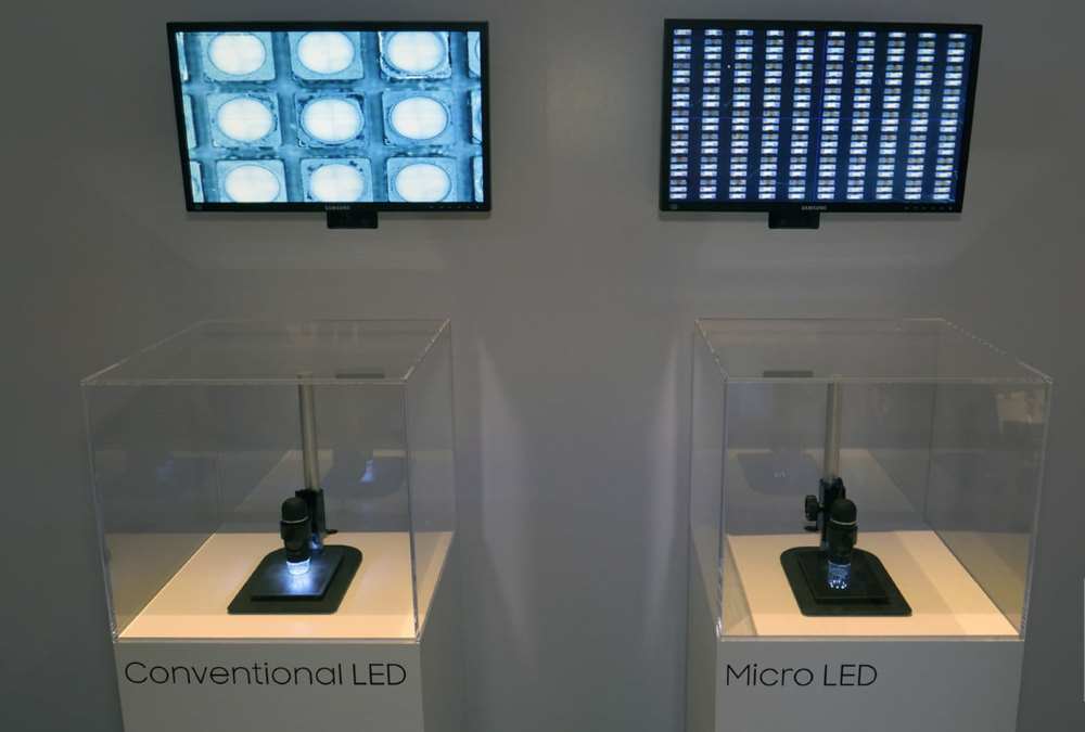
So, you probably heard about the MicroLED technology, but if you did not, here is a small refresher: it is a new display technology based on GaN (Gallium Nitride) that offers more than what we have nowadays with OLED and LCD. It presents more durability than OLED, delivering those perfect dark colors with no danger of burn-in after a long time, it can be brighter than any other technology on the market, with better color quality, faster display switching speeds, and better energy efficiency.
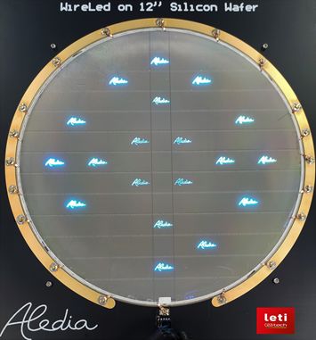
Even though it has already caught the eye of TV manufacturers and co., it still is not a sounding name on the market, alongside, for example, OLED, but why? Being a new technology, its manufacturing process is still a bit blurry, with companies such as Aledia trying to find the best way to enable the mass production that will allow the technology to strive on the market. As such, Aledia came through with the world’s first MicroLED production on 300 mm silicon wafers, which only has been done on 200 mm wafers to this point. The larger wafer size means lower transfer and assembly costs.
To analyze the issue with producing larger wafers, we must take a look at its production process. Planar or “2D” microLEDs are produced by depositing flat layers of GaN, mainly on small 100mm sapphire wafers, due to the stress seen on the microLEDs when the wafer size is increased. With “3D” microLED technology, developed by them, this fabrication process can be performed in bigger and silicon wafers, meaning the silicon foundries can aid in their production.
Having these two breakthroughs combined together, is there some hope to see this technology soon in our everyday lives? Well, the use of larger silicon wafers and making use of the silicon foundries to provide the high demands of the industry are two steps in the right direction. But, there is a need of around 24 million 300 mm wafers per year. Will we see it any time soon? Only time will tell, but one can hope.
Aledia company link: https://www.aledia.com/en


