Non-inverting OPAMP
Introduction The voltage signal applied to an op-amp can either be supplied to its non-inverting input (+) or the inverting input (-). These different configurations are simply known as a non-inverting op-amp, and inverting op-amp.
Introduction
The voltage signal applied to an op-amp can either be supplied to its non-inverting input (+) or the inverting input (-). These different configurations are simply known as a non-inverting op-amp, and inverting op-amp. In this tutorial, we focus on the non-inverting configuration and present its details.
An overview of the non-inverting op-amp will be given in the first section through the concept of the ideal amplifier.
In the second section, real non-inverting configurations are discussed, we demonstrate the equations describing the gain and the input/output impedances.
Finally, examples of circuits based on the non-inverting configurations are given in the last section.
Ideal non-inverting op-amp
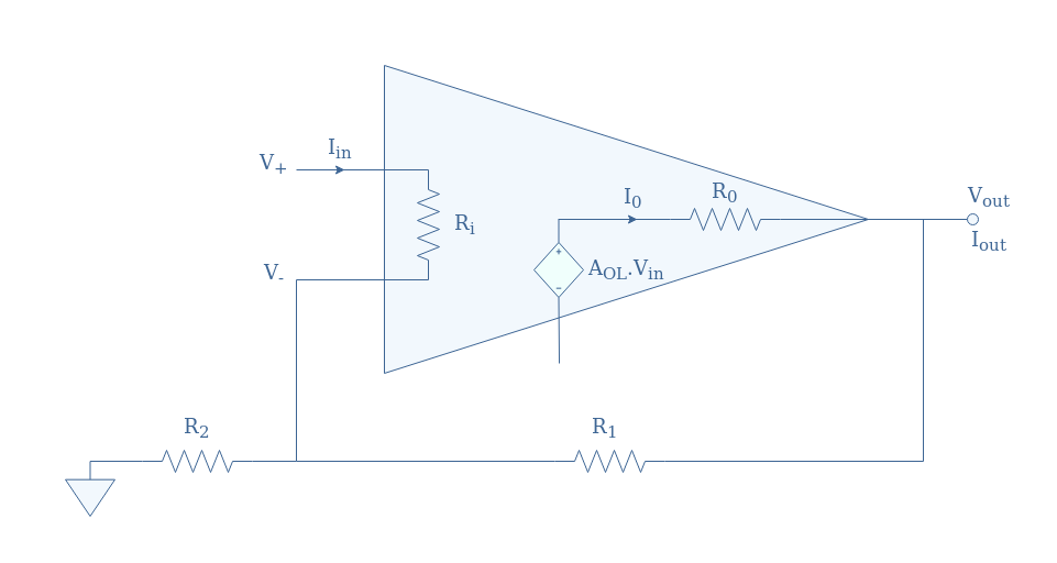
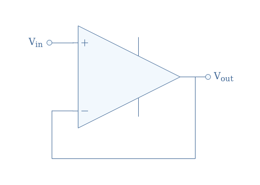
The goal of this section is to properly demonstrate and explain the ideal characteristics of the non-inverting configuration such as its input/output impedance and gain. The circuit representation of an ideal non-inverting op-amp is given in Figure 1 below.
Note that the symbol “∞” highlights the fact that the op-amp is here to be considered ideal. We highly recommend the reader to refer to the tutorial Op-amp basics for this section.
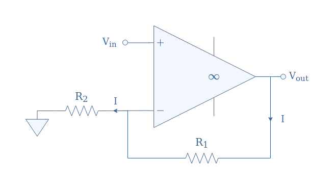
In this ideal model, the input impedance defined by the contribution of the resistance linking the inverting and non-inverting inputs (Ri in Figure 3) and the resistors R1 and R2, is infinite. Moreover, for an ideal circuit, Ri is supposed to be infinite, as a consequence, no currents can enter the op-amp through any input because of the presence of an open circuit.
This observation can also be summarized by saying that the node interconnecting the inverting input and resistances R1 and R2 is a virtual short. For this same reason, all the feedback current across R1 (I) is also found across R2.
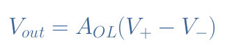
For the ideal model, the equality V+=V–=Vin is assured by the fact that the differential signal V+-V– can only be equal to 0 in order to produce a finite output Vout when multiplied by an infinite open-loop gain.
We can see the branches connected to the inverting input acting as a voltage divider circuit:
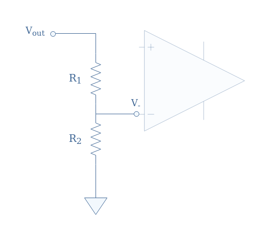
According to the voltage divider formula, we can express the inverting voltage V– as a function of the output voltage and the resistances:
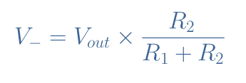
Since V–=Vin, after some simplification, we prove the expression of the gain in closed-loop ACL of an ideal non-inverting configuration:
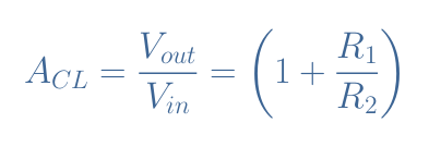
We can note that the ideal gain presented in Equation 2 is strictly positive and higher than 1, meaning that the output signal is amplified and in phase with the input signal.
Real non-inverting op-amp
In a real op-amp circuit, the input (Zin) and output (Zout) impedances are not idealized to be equal to respectively +∞ and 0 Ω. Instead, the input impedance has a high but finite value, the output impedance has a low but non-zero value.
The non-inverting configuration still remains the same as the one presented in Figure 1.
Closed-loop gain
For a non-inverting configuration, Equation 1 still applies for V– , moreover, we have V+=Vin. However, since a low current can flow from the non-inverting input to the inverting input, the voltages are not equal anymore: V+≠V–.
We also need to remind that the inputs V+ and V– are linked with the output through the open-loop gain formula:
The equations for V+ and V– can be injected in Equation 3. After regrouping the terms “Vout” on one side of the equation and the terms “Vin” on the other, we get:
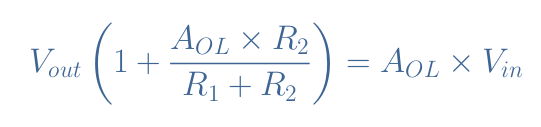
Finally, the closed-loop gain ACL for a real non-inverting configuration is given by Equation 4:
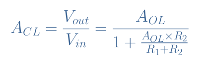
For a real configuration, the gain not only depends on the resistor values but also on the open-loop gain
It is interesting to note that if we consider the op-amp to be ideal (AOL→+∞), the denominator is simplified to one term: AOLR2/(R1+R2). As a consequence, Equation 4 is simplified back to Equation 2.
Output impedance
We start by assuming the equality of the currents across the resistances: IR1=IR2. Even if for real op-amps, a small leaking current enters the inverting input, it is several orders of magnitude smaller than the feedback current.
The current I0 across R0 (see Figure 3) can be expressed as a function of the voltage drop across R0 and the same value of the impedance R0:
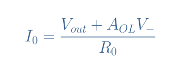
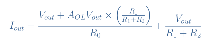
Since V– is described by Equation 1, the output current Iout can be expressed as the sum of I0 and the current flowing in the feedback branch given by Vout/(R1+R2):
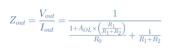
Finally, after rearranging the equation to obtain the ratio Zout=Vout/Iout, we can write the expression of the output impedance for a real non-inverting configuration:
We can note that in the case of an ideal op-amp, that is to say when AOL→+∞, we observe indeed Zout→0.
A simplified version for the expression of Zout is given by the following Equation 6:
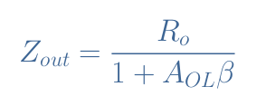
The term β is known as the feedback factor and is given by the ratio R1/(R1+R2). With that simplified version, we can still see that Zout→0 for an ideal op-amp situation.
Input impedance
The input impedance of a non-inverting configuration can be defined by the ratio V+/Iin (see Figure 3). For the input loop, we can write Kirchoff’s voltage law such as V+-Vin+IR2R2=0 with IR2 being the current across the resistor R2.
It can be shown that the expression of the input impedance can also be written as a function of the feedback factor:
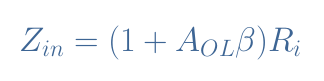
Again, when the ideal situation is satisfied (AOL→+∞) we find that Zin→+∞ such as specified in the first section.
Non-inverting op-amp examples
Buffer circuits
The most simple designs for non-inverting configurations are buffers, which have been described in the previous tutorial Op-amp Building Blocks. In this configuration, R1=0 and R2→+∞ as we can present in Figure 4 below:
This buffer (or voltage follower) has a unity gain and does not invert the output, meaning that Vout=Vin. Its high input impedance and low output impedance are very useful to establish a load match between circuits and make the buffer to act as an ideal voltage source.
Example
We consider a real non-inverting configuration circuit given in Figure 5:
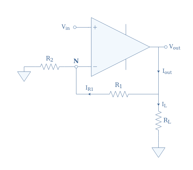
The resistors, input value, and gain in open-loop are given such as:
- R1=10 kΩ
- R2=2 kΩ
- RL=1 kΩ
- Vin=1 V
- AOL=105
First of all, we can compute the value of the closed-loop gain ACL. By using Equation 4 we obtain ACL=5.99 while Equation 2 gives ACL=6. We can remark that both values are very similar since AOL is high. Typical values of AOL for real op-amps range between 2×10⁴ and 2×10⁵, which is high enough to always consider Equation 2 valid.
From this value, we can simply say that the output voltage is given by Vout=ACL×Vin= 6 V.
The currents IR1 (across R1) and IR2 (across R2) are approximately equal if we consider the leaking current in the inverting input to be much lower than the feedback current. Due to the virtual short existing at the node N, VN=Vin, and therefore we have IR1=IR2=Vin/R2=0.5 mA.
Since the current IL through the output load is given by Vout/RL=6 mA, we can determine the output current thanks to Kirchoff’s current law: Iout=IL+IR1=6.5 mA.
Finally, we can also specify the output impedance to be Zout=Vout/Iout=920 Ω.
Conclusion
When the input signal is supplied to the pin “+”, the op-amp is said to be in a non-inverting configuration. The design and main properties of this configuration are presented in the first section that presents its ideal model.
In the second section, the real non-inverting op-amps are presented. Due to the parasitic phenomena that are intrinsic to their design, their properties change, the expression of the closed-loop gain, input, and output impedances are different. However, the simplified version of these formulas that describe the ideal model can indeed be recovered when we set the open-loop gain to be infinite.
Examples of real configurations are shown in the last section, we present how to calculate the main characteristics of a configuration with the knowledge of the resistors value and input voltage.


The voltage divider formula near the top is incorrect. It should be, V- = Vout*(R2/(R1+R2)). Otherwise, very well written with clear explanations in step-by-step analysis.
Thanks for pointing us to this. It’ fixed on the article 🙂
Still not fixed after 3 months.
It’s corrected now, could you check?