Cadence and Skywater Detail Next Open Multi-Project Wafer Shuttle Program
The program offers cost-effective access to the 130 nm CMOS process, enabling students, researchers, and start-ups to tapeout complex mixed-signal designs using commercial-grade and open-source tools.
The collaborative Multi-Project Wafer (MPW) aggregation service between Cadence Design Systems and Skywater Technology has opened the submission window for its next shuttle run on the SKY130 open-source process. This initiative provides engineers, researchers, and early-stage start-ups with a standardized path to silicon fabrication on a mature, commercially relevant process node. The core value proposition is the utilization of the fully open-source SKY130 Process Design Kit (PDK), which eliminates the need for a non-disclosure agreement and integrates with both commercial and community-developed Electronic Design Automation (EDA) flows.
Design submissions for the newly launched shuttle run are open through January 16, 2026. Image used courtesy of Cadence Academic Network
SKY130, an Open-Source Foundry Process Design Kit
The MPW service utilizes Skywater’s established 130 nm CMOS technology. The 130 nm node remains highly relevant as a cost-effective, proven workhorse for mixed-signal applications, including analog, RF, and specialized sensors. The PDK, released in collaboration with Google and Efabless, offers a substantial advantage for design iteration and education due to its unrestricted availability.
The service offers two process options for the upcoming shuttle: a standard offering and one that includes embedded resistive random-access memory (ReRAM). The ReRAM option expands the design space by providing non-volatile memory integration for low-power and edge computing applications.
Design Requirements and Technical Constraints
Designs submitted to the Cadence MPW service must adhere to precise specifications to ensure manufacturability and fit within the allocated real estate on the wafer. Submissions must also utilize the latest version of the SKY130 PDK, which is updated regularly by the open-source community. Designers are responsible for ensuring the functionality and performance of their circuit designs after meeting the manufacturability checks.
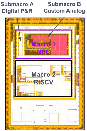
North Carolina State University student project combining a mixed-signal NFC tag with a Rocket Chip RISC-V processor. Image used courtesy of Cadence Design Systems
EDA Tools and Design Flow
A key feature of the MPW aggregation service is its flexibility regarding the EDA environment. The service accepts final OASIS design files regardless of the tools used to create them, supporting designers who utilize both commercial and open-source tools.
Designers can leverage Cadence’s professional-grade tools, often accessed through academic programs, to manage complex flows, verification, and physical implementation. Additionally, the open nature of the PDK facilitates integration with community-developed tools such as the OpenLane flow and other ecosystem elements (e.g., Caravel platform), lowering the overhead associated with licensing proprietary software.
This dual-tooling support helps bridge the gap between academic and professional design methodologies, allowing engineers to gain experience with industry-standard flows while retaining the freedom of open-source resources.
Skywater SKY130 PDK design resources are available for download from various repositories. Image used courtesy of Skywater Technology
Timeline and Costs
The official submission window for design files is open, with a deadline of January 16, 2026. Following submission, designers can expect feedback on their tapeout package within two weeks. The expected die delivery is targeted for July 2026, though this timeline remains subject to Skywater’s fabrication queue and scheduling. The cost for submitting a design block ranges from $10,000 to $12,000 (plus applicable taxes, shipping, and handling), with the price variation corresponding to the choice of the standard or ReRAM-enabled process option. This fixed cost model significantly reduces the financial barrier associated with full mask-set fabrication.
The availability of this service underscores a growing industry trend toward democratizing silicon access, lowering the initial capital expenditure required for prototyping complex integrated circuits. The SKY130 MPW shuttle provides students, researchers, and start-ups with a clear and technically supported path to realize their designs in silicon, using a commercially viable 130 nm CMOS platform suitable for mixed-signal SoCs, low-power embedded microcontrollers, IoT sensor interfaces, and specialized RISC-V processor cores. The prior shuttle successfully fabricated designs ranging from dual-core RISC-V systems-on-chip to near-field communication tags and environmental sensors, demonstrating the platform’s utility across diverse, market-relevant applications.


