Google and SkyWater Technology collaborate to launch an Open-Silicon developer portal
With the exponential increase in the demand and requirement of silicon-based chips, Google, in partnership with SkyWater Technology, has launched a new platform to encourage and help the developer community to get started with its Open MPW shuttle program. Leveraging SkyWater’s open-source process design kit (PDK), the platform allows developers to submit open-source integrated circuit designs to get manufactured at zero cost.
With the exponential increase in the demand and requirement of silicon-based chips, Google, in partnership with SkyWater Technology, has launched a new platform to encourage and help the developer community to get started with its Open MPW shuttle program. Leveraging SkyWater’s open-source process design kit (PDK), the platform allows developers to submit open-source integrated circuit designs to get manufactured at zero cost. Therefore, the partnership marks a major breakthrough for the open silicon ecosystem, enabling customers to develop complex and advanced silicons with ease.
Along with Moore’s law termination and the upsurge of connected devices (IoT), there is a significant need to discover more sustainable methods to expand computing. Moving toward more efficient dedicated hardware accelerators is what we need to do instead of just packing more transistors into smaller areas. Due to recent challenges with the global chip supply chain, consumers have seen significant rising prices, shortages, queues, and scalping. Hence, we must accomplish this by using more of the existing global foundry capacity, which provides access to older and proven process node technology.
Recommended reading: EFABLESS LAUNCHES CHIPIGNITE WITH SKYWATER TO BRING CHIP CREATION TO THE MASSES
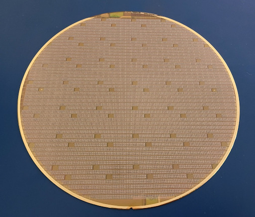
The SKY130 process node (a 130nm technology), enables the development and prototyping of IoT applications that often need to maintain a balance between cost, power, and performance while including an amalgamation of analog blocks and digital logic. The availability of an open-source and manufacturable PDK alters the status quo in the custom silicon design industry and academia. Designers are now free to start their projects without the constraints of NDAs or usage limitations. Further, the open-source platform enables peer developers to replicate complex designs.
“By combining open access to PDKs, and recent advancements in the development of open-source ASIC toolchains like OpenROAD, OpenLane, and higher-level synthesis toolchains like XLS, we are getting us one step closer to bringing software-like development methodology and fast iteration of cycles to the silicon design world. We believe we are at the edge of a similar revolution for custom accelerator development, where hardware designers compete by building on each other’s works rather than reinventing the wheel”, claims Johan Euphrosine.
Previous versions of the Open MPW Shuttle Program received contributions varying from the Microwatt OpenPOWER 64-bit core to RISC-V cores to Sudoku accelerators, hardware implementations of games, SRAM/ReRAM generators, and other small ASICs. The design submissions also included crypto and ML operations accelerators along with multiple group submissions.
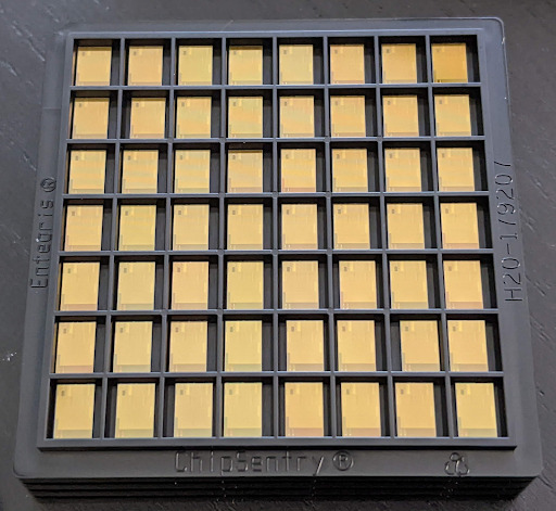
With this collaboration, the end-user can avail the advantage of a standardized 2.92mm x 3.52mm user area and 38 I/O pins for each project. The design can be hardened by a predefined harness. Additionally, the platform also provides the necessary test infrastructure to test and validate the chip specifications before submitting the design for tape out.
Google has launched its new developer portal that provides instructions to get started with various tools of the open-source silicon ecosystem. To get started on your silicon journey, check out the Google Open-Source Blog.