Simple circuit lets you characterize JFETs
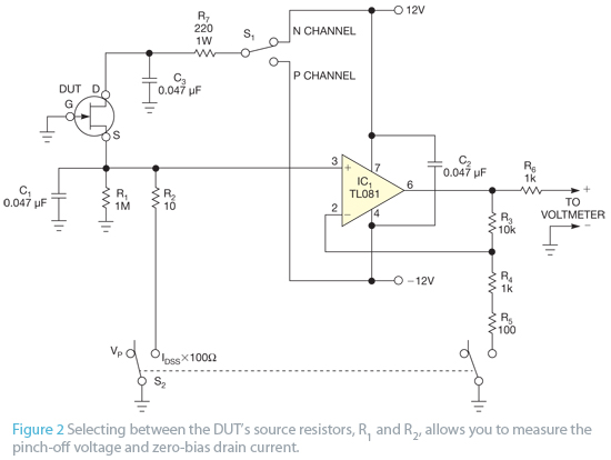
by John Fattaruso @ edn.com: When working with discrete JFETs, designers may need to accommodate a large variation in device parameters for a given transistor type. A square-law equation is usually used as an approximate model for the drain-current characteristic of the JFET: ID=β(VGS−VP)2, where ID is the drain current, VGS is the gate-to-source voltage, β is the transconductance parameter, and VP is the gate pinch-off voltage.
by John Fattaruso @ edn.com:
When working with discrete JFETs, designers may need to accommodate a large variation in device parameters for a given transistor type. A square-law equation is usually used as an approximate model for the drain-current characteristic of the JFET: ID=β(VGS−VP)2, where ID is the drain current, VGS is the gate-to-source voltage, β is the transconductance parameter, and VP is the gate pinch-off voltage. With this approximation, the following equation yields the zero-bias drain current at a gate-to-source voltage of 0V: IDSS=βVP 2, where IDSS is the zero-bias drain current.
Simple circuit lets you characterize JFETs – [Link]


