Texas Instruments TPS258x-Q1 Integrated USB Charging Port Solution
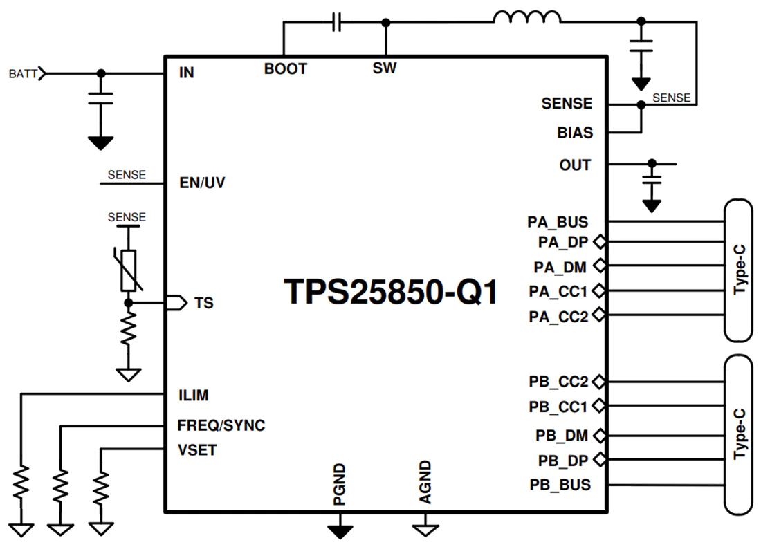
Texas Instruments TPS258x-Q1 Integrated USB Charging Port Solution integrates a monolithic, synchronous, rectified, step-down, switch-mode converter with internal power MOSFETs. It also includes two USB current-limit switches with charging port auto-detection.
Texas Instruments TPS258x-Q1 Integrated USB Charging Port Solution integrates a monolithic, synchronous, rectified, step-down, switch-mode converter with internal power MOSFETs. It also includes two USB current-limit switches with charging port auto-detection. The TPS2585x-Q1 offers a compact solution that achieves 6.6A of continuous output current with excellent load and line regulation over a wide input supply range. The synchronous buck regulator operates with peak-current mode control and is internally compensated to simplify the design. A resistor on the FREQ pin sets the switching frequency between 200kHz and 3MHz. Operating below 400kHz results in better system efficiency, and operation above 2.1MHz avoids the AM radio bands and allows for use of a smaller inductor.
The Texas Instruments TPS2585x-Q1 integrates standard USB Type-C port controller functionality that includes Configuration Channel (CC) logic for 3A and 1.5A current advertisement. Battery Charging (Rev. 1.2) integration provides the required electrical signatures necessary for non-Type-C, legacy USB devices that use USB data line signaling to determine USB port current sourcing capabilities. The TPS2585x-Q1 also has integrated VCONN power that can meet the USB3.1 power requirement. The part is especially suitable for dual-port applications due to the high system integration and small footprint.
The TPS2585x-Q1 provides various safety features for USB charging and system operations. These include external negative thermistor monitoring, cycle-by-cycle current limit, hiccup short-circuit protection, undervoltage lockout, BUS overcurrent, OUT overcurrent, and die overtemperature protection. The device family is available in a 25-pin, 3.5mm x 4.5mm QFN package.
Features
- AEC-Q100 qualified for automotive applications
- –40°C to +125°C TA temperature grade 1
- HBM ESD classification level H2
- CDM ESD classification level C5
- Synchronous buck regulator
- High efficiency at 2.1MHz: 93.4% at VIN = 13.5V, IPA_BUS = 3A and IPB_BUS = 3A
- 18mΩ/10mΩ Low RDS(ON) buck regulator MOSFETs
- 5.5V to 26V, withstand 36V input operating voltage range
- 200kHz to 3MHz adjustable frequency
- FPWM with spread-spectrum dithering
- Selectable output voltage (5.1V, 5.17V, 5.3V, 5.4V)
- Internal power path
- 7mΩ/7mΩ Low RDS(ON) internal USB power MOSFETs
- ±10% at 3.4A programmable current limit for USB ports with high accuracy:
- OUT: 5.1V, 200mA supply for auxiliary loads
- 90mV at 2.4A load line drop compensation
- Compliant to USB-IF standards
- Type-C rev 1.3
- 3A capability advertisement on CC
- VBUS application and discharge
- 200mA VCONN source
- Automatic DCP modes (TPS25850-Q1)
- Shorted mode per BC1.2 and YD/T 1591 2009
- 1.2V Mode
- 2.7V Divider 3 mode
- Type-C rev 1.3
- Load shedding versus programmable TA
- –40°C to +150°C device TJ range
Simplified Schematic
more information: https://www.ti.com/product/TPS25850-Q1


