Advanced protoboard layout with 1.27mm pitch for smd parts
Main Features Plated through holes in standard 2.54mm raster like on traditional protoboard Pads for smd parts in 1.27mm raster in between SOIC parts can directly be used without adapters SMD pads are not contacted to the other side: Different tracks can either cross each other or connect No wires to solder in like on non-plated-through protoboard Allows for much more dense layout You can build your own protoboard for SMD component using the production file on github.com
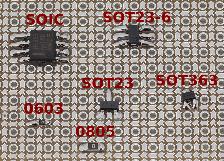
Main Features
- Plated through holes in standard 2.54mm raster like on traditional protoboard
- Pads for smd parts in 1.27mm raster in between
- SOIC parts can directly be used without adapters
- SMD pads are not contacted to the other side:
- Different tracks can either cross each other or connect
- No wires to solder in like on non-plated-through protoboard
- Allows for much more dense layout
You can build your own protoboard for SMD component using the production file on github.com


hi,
so can you actually BUY these protoboards?
BD
How many do you need?