Making your first Circuit Board – Getting started with PCBway [Part 2]
This is the next part of "MAKING YOUR FIRST PRINTED CIRCUIT BOARD - GETTING STARTED WITH PCBWAY [Part 1]" Series. Designing your PCB When you design your first PCB, there will be several steps that you will need to take before you sent the design files off to the manufacturer for manufacturing.
This is the next part of “MAKING YOUR FIRST PRINTED CIRCUIT BOARD – GETTING STARTED WITH PCBWAY [Part 1]“ Series.
Designing your PCB
When you design your first PCB, there will be several steps that you will need to take before you sent the design files off to the manufacturer for manufacturing.
Create The Schematic
When creating the schematic in any of the programs mentioned in part 1, remember to double check that everything is connected where it needs to be with a NET. This is how the program’s auto-routing, DRC, and ERC features know what is connected where. I generally like to go over my schematic two or three times, counting each net, and making sure that everything is connected and accounted for before moving on to the board layout.
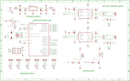
When designing your schematic, you will need to pay particular care to ensure that the footprint of the component you use in the schematic exactly matches the footprint of the component that will be soldered to the PCB.
Creating the PCB
Each PCB CAD software will usually offer a way for you to transfer your schematic design to a PCB layout. Designing a PCB layout might be slightly tedious if it’s your first time doing it, but fortunately, several tutorials talk about it. If your design features mounting holes, v-scores, mouse bites, or fingers, make sure you place them on the board first.
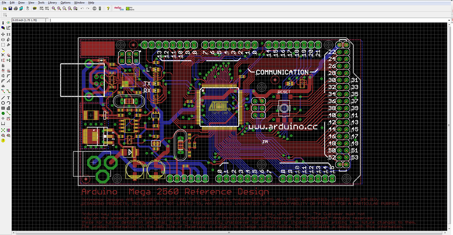
When designing your PCB Layout, it is essential that you take note of your traces size. Manufacturers usually have restrictions on how small your traces can be, as well as how small the clearances can be between traces. PCBWay minimum track and spacing are 4mil and 4 mil respectively, their minimum hole size is 0.2mm. Of course, going for the minimum will slightly increase your board cost.
Having your PCB manufactured
The first thing you will need to do before you can ship your design off to be manufactured is to generate a Gerber file that contains all of the necessary design files to use in the PCBs production. This file is a universal file and is generated in the CAD program you used to design your PCB. Each program has its way of generating this file, so be sure to read the program’s instructions, or search for the proper way to create the file with the program you are using.
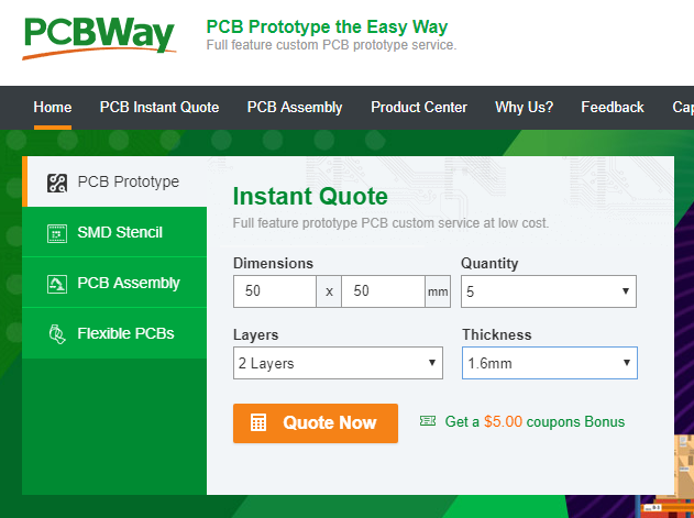
Ordering at PCBWay
Go to PCBWay (https://www.pcbway.com) and fill the board details in the instant order, from there you will be directed to more elaborate board details.
Update your board requirement information in the PCB Specification screen. You can change the board thickness, board color, silk color, and even the type of finish you want. Some of these add-ons are going to increase the board cost.
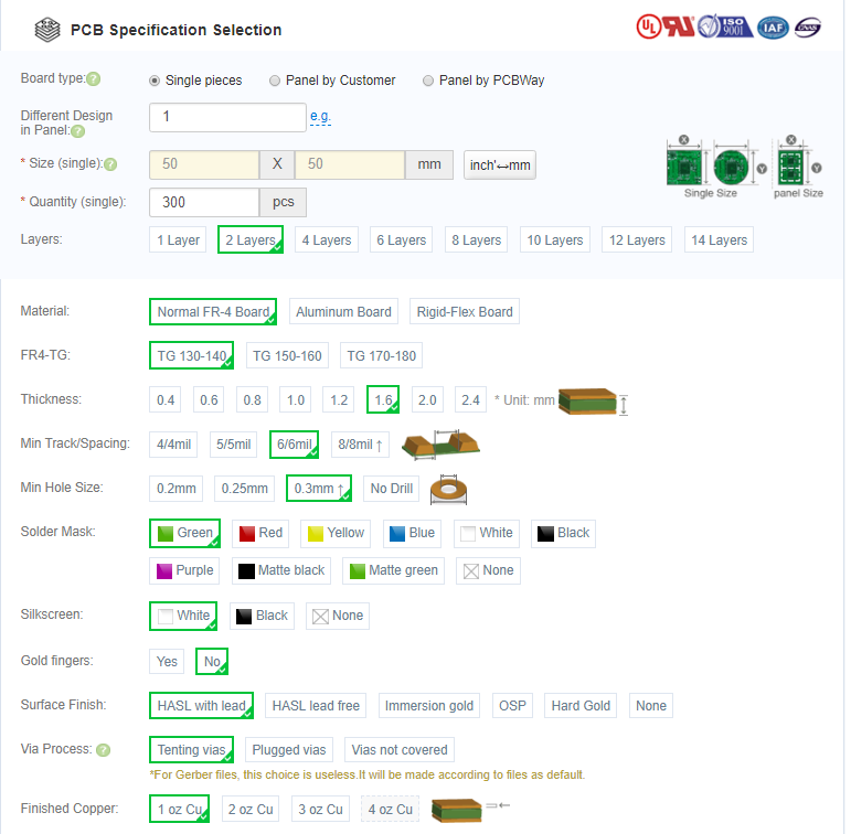
Once you have all of the various options for your PCB selected, all that is left is to add to cart, upload your Gerber files, make payment, and wait for your PCBs to arrive. It could take anywhere from 3 – to 6 days to be produced depending on the number of your boards.
One major advantage of using PCBway is that – they offer a free engineering file review service. Before your board goes into manufacturing their team of professional technicians will review your design for any potential errors.


