SUNY Polytechnic Creates 3-in-1 Device That Can Be A Diode, A MOSFET And A BJT
In a recently published study, a team of researchers at SUNY Polytechnic Institute in Albany, New York, has suggested that combining multiple functions in a single semiconductor device can significantly improve device's functionality and efficiency. Nowadays, the semiconductor industry is striving to scale down the device dimensions in order to fit more transistors onto a computer chip and thus improve the speed and efficiency of the devices.
In a recently published study, a team of researchers at SUNY Polytechnic Institute in Albany, New York, has suggested that combining multiple functions in a single semiconductor device can significantly improve device’s functionality and efficiency.
Nowadays, the semiconductor industry is striving to scale down the device dimensions in order to fit more transistors onto a computer chip and thus improve the speed and efficiency of the devices. According to Moore’s law, the number of transistors on a computer chip cannot exponentially increase forever. For this reason, scientists are trying to find other ways to improve semiconductor technologies.
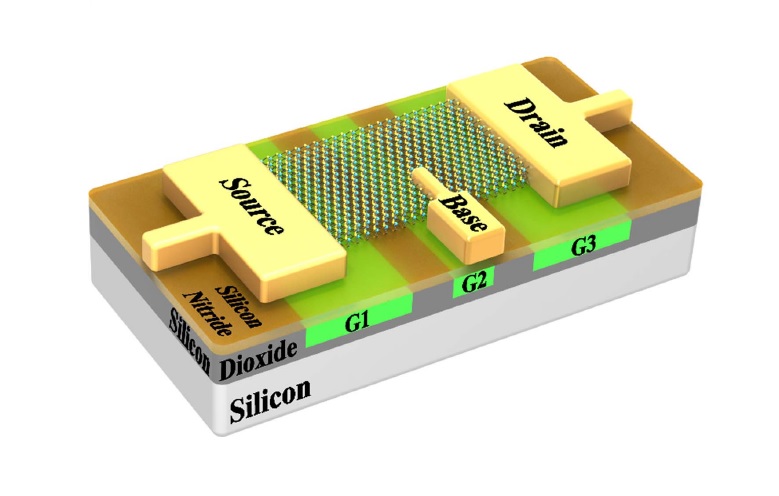
To demonstrate the new technology which can be an alternative to Moore’s law, the researchers of SUNY Polytechnic designed and fabricated a reconfigurable device that can be a p-n diode (which functions as a rectifier), a MOSFET (for switching), and a bipolar junction transistor (or BJT, for current amplification). Though these three devices can be fabricated individually in modern semiconductor fabrication plants, it often becomes very complex if they are to be combined.
Ji Ung Lee at the SUNY Polytechnic Institute said,
We are able to demonstrate the three most important semiconductor devices (p-n diode, MOSFET, and BJT) using a single reconfigurable device. We can form a single device that can perform the functions of all three devices.
The multitasking device is made of 2-D tungsten diselenide (WSe2), a new transition metal dichalcogenide semiconductor. This class of materials is special as the bandgap is tunable by varying the thickness of the material. It is a direct bandgap while in single layer form.
Another challenge was to find a suitable doping technique as WSe2 lacks one being a new material. So, to integrate multiple functions into a single device, the researchers developed a completely new doping method. By doping, the researchers could obtain properties such as ambipolar conduction, which is the ability to conduct both electrons and holes under different conditions. Lee said,
Instead of using traditional semiconductor fabrication techniques that can only form fixed devices, we use gates to dope.
These gates can control which carriers (electrons or holes) should flow through the semiconductor. In this way, the ambipolar conduction is achieved. The ability to dynamically change the carriers allows the reconfigurable device to perform multiple functions. Another advantage of using gates in doping is, it saves overall area and enable more efficient computing. As consequence, the reconfigurable device can potentially implement certain logic functions more compactly and efficiently.
In future, researchers plan to investigate the applications of this new technology and want to enhance its efficiency further. As Lee said,
We hope to build complex computer circuits with fewer device elements than those using the current semiconductor fabrication process. This will demonstrate the scalability of our device for the post-CMOS era.


