Digital Buffer
Digital Buffer The digital buffers are used in digital circuits for the amplification of digital signals in order to drive high current loads. Besides current amplification, the digital buffers provide isolation between input and output circuits where output is connected to some high-power load such as a relay, lamp or solenoid, etc.
Digital Buffer
The digital buffers are used in digital circuits for the amplification of digital signals in order to drive high current loads. Besides current amplification, the digital buffers provide isolation between input and output circuits where output is connected to some high-power load such as a relay, lamp or solenoid, etc. The digital device used for such purposes is called Digital Buffer.
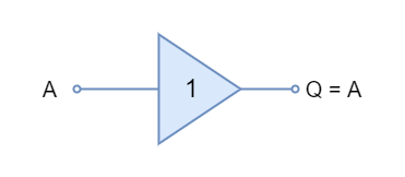
The digital buffer is similar to the logic “NOT” gate in a way that it is a two-terminal device having input and output terminals only. However, the logic “NOT” gate complements the input signal at its output. As discussed in the logic “NOT” gate article, when the input of a “NOT” gate is “HIGH” then its output will NOT be “HIGH”. Likewise, when the input of a “NOT” gate is “LOW” then its output will NOT be “LOW”. On the other hand, the digital buffer does not complement the input signal at its output. The input signal is reflected at the output of a digital buffer without any change in its logic. The digital buffer is a non-inversion logic and follows Idempotent Law. Its Boolean expression is given below:
Q = A
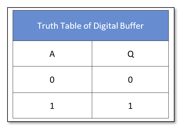
From the expression, it is eminent that the output (Q) state of a digital buffer is only true when the input (A) is true otherwise the output (Q) is false. The symbol and truth table of a digital buffer is shown below:
Construction using NOT Gates
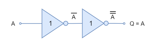
The digital buffer can be constructed using a basic logic “NOT” gate. The connection of two logic “NOT” gates back-to-back in series form a Digital Buffer. First, the “NOT” gate inverts the input signal, and second, “NOT” inverts the inverted signal back to the original input signal. The process of “double inversion” leads to the formation of a Digital Buffer.
Digital Buffer Fan-out
The Digital Buffer is used in digital circuits even though it does not perform any logic or decision. The Digital Buffer is useful in the isolation or separation of two circuits whereas the impedance of the input circuit does not affect the impedance of the output circuit. Moreover, it can be used to drive high current loads such as switches or relays, etc. This means that Digital Buffers have the “fan-out” capability to deliver high power to the output loads.
The “fan-out” is the ability of a Digital Buffer or Digital I.C. to deliver high output current to a load. It is simply, the capability to amplify the input signal at its output after performing any due logic. The output of a logic gate may need to be connected to a high current LED, switch or relay and in such a case a logic gate with a high “fan-out” is required. Usually, the output of a logic gate is connected to the input of another logic gate and it requires a nominal current to drive another gate’s input. When a number of inputs (logic gates) are connected to the output of a logic gate then additional current is required which depends upon a number of factors such as the number of inputs and their circuit types etc. In simple words, it can be said that the “fan-out” is the number of parallel connections that can be efficiently driven by a logic gate or Digital Buffer.
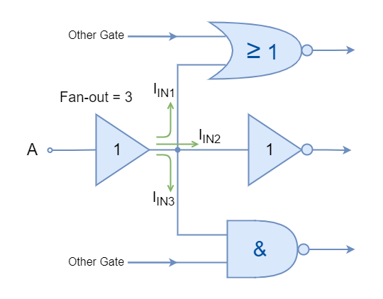
Generally, a Digital Buffer can have a high “fan-out” rating of 20 to drive parallel connections of the same logic family. A Digital Buffer with a high fan-out (current source) rating also carries a high fan-in (current sink) rating. However, there is a limitation to the number of devices that can be connected to the input or output of a logic gate due to propagation delay. The propagation delay is a function of the number of connections taken out of a terminal and it deteriorates with the increase in the number of signals.
Tri-state Buffer
The Tri-state Buffer, as the name says, has three states that can be achieved by an electronic controller connected to an input terminal of Digital Buffer. The Tri-state Buffer is used in circuits where decoupling of input and output circuits is essentially required. It is a device similar to the Digital Buffer but has three terminals and the additional (third) terminal is used to control the output of Digital Buffer. Additionally, it has three states compared to the two states of a Digital Buffer.
The Tri-state Buffer’s output (Q) can be put into any of the three states by electronically driving its “Control” or “Enable” terminal to logic “LOW” or “HIGH”. It can be thought of as an input controller switch which is demonstrated in the following figure.
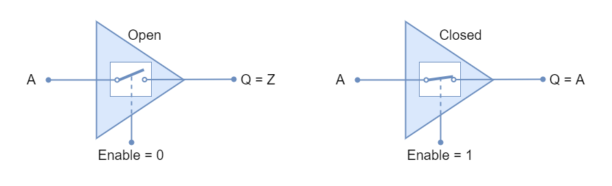
The Tri-state buffer can be activated or deactivated using the “Enable” terminal. When enabled, the Tri-state Buffer reflects the input signal towards the output without any change just like a Digital Buffer. Whereas, when Tri-state Buffer is disabled then path between input and output becomes open-circuited and leads to a high impedance state “Hi-Z”. This high impedance state “Hi-Z” is the third-state besides logic “HIGH” and “LOW” states. Because of these three states, it is called a Tri-state Buffer.
In the high impedance “Hi-Z” state, a high impedance appears between input and output leading to electrical isolation. In this state, no current flows in the input and from the output.
The Tri-state Buffer discussed above is an Active “HIGH” Tri-state Buffer as it becomes active when “Enable” is at a “HIGH” state. Another variant is an Active “LOW” Tri-state buffer which gets activated when “Enable” is at a “LOW” state. These Tri-state Buffers are non-inverting when enabled and reflect the input signal at the output without inversion. However, Tri-state inverting Buffers are also commercially available which inverts the input signal at the output. They are also available in Active “HIGH” inverting and Active “LOW” inverting Tri-state Buffer variants. These four types of Tri-state Buffer variants are explained below along with their truth tables.
Active “HIGH” Tri-state Buffer
The symbol and truth table of Active “HIGH” Tri-state Buffer is shown below:
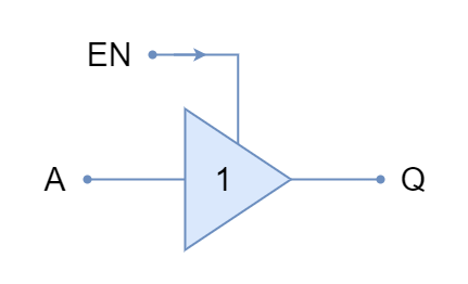
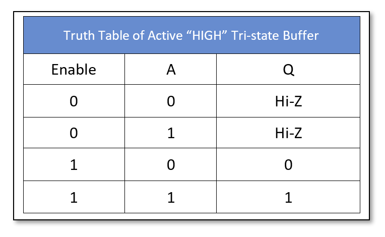
The active “HIGH” Tri-state Buffer is commercially available as 74LS241 with octal buffers. It is active when the “Enable” terminal is at a “HIGH” state and passes the input signal towards the output unaltered. When the “Enable” terminal is at the “LOW” state then Tri-state Buffer becomes disabled and a high impedance state “Hi-Z” appears at the output.
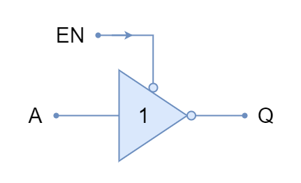
Active “LOW” Tri-state Buffer
The symbol and truth table of Active “LOW” Tri-state Buffer is shown below:
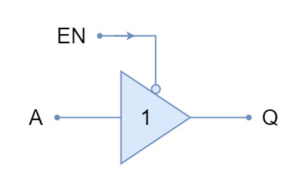
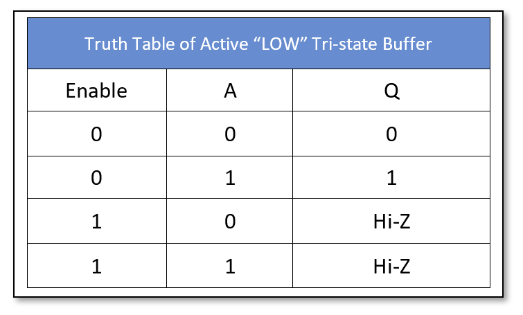
The active “LOW” Tri-state Buffer is active when the “Enable” terminal is at a “LOW” state and passes the input signal towards the output unaltered. When the “Enable” terminal is at the “HIGH” state then Tri-state Buffer becomes disabled and a high impedance state “Hi-Z” appears at the output. The “Inversion Bubble” at the terminal of “Enable” indicates an active “LOW” input.
Active “HIGH” Inverting Tri-state Buffer
The symbol and truth table of Active “HIGH” Inverting Tri-state Buffer is shown below:
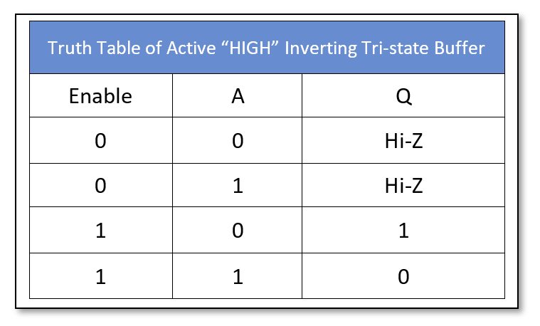
The active “HIGH” Tri-state Buffer is commercially available as 74LS240 with octal buffers. It is active when the “Enable” terminal is at a “HIGH” state and passes the input signal towards the output after inversion. When the “Enable” terminal is at the “LOW” state then Tri-state Buffer becomes disabled and a high impedance state “Hi-Z” appears at the output. The “Inversion Bubble” at the output terminal indicates an inversion of the input.
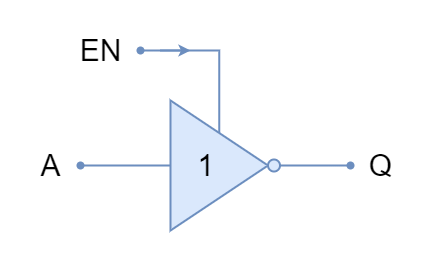
Active “LOW” Inverting Tri-state Buffer
The symbol and truth table of Active “LOW” Inverting Tri-state Buffer is shown below:
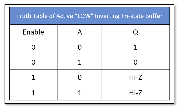
The active “LOW” Tri-state Buffer is active when the “Enable” terminal is at a “LOW” state and passes the input signal towards the output after inversion. When the “Enable” terminal is at the “HIGH” state then Tri-state Buffer becomes disabled and a high impedance state “Hi-Z” appears at the output. The “Inversion Bubble” at the output terminal indicates an inversion of the input. Whereas, “Inversion Bubble” at the terminal of “Enable” indicates an active “LOW” input.
Tri-state Buffer as Bus Controller
The Tri-state Buffers are used in many electronic and digital circuits to control access to the data buses allowing multiple devices to be connected to the single data bus. The data buses exist between microprocessors, peripherals, I/O or memory chips, etc. and multiple devices interface with them. The multiple devices connected with the same bus tries to fetch the bus to “LOW” or “HIGH” creating a contention. The contention is said to occur when some of the devices try to pull up (HIGH) the bus whilst at the same time some devices try to pull it down (LOW). This would create a condition of short-circuiting and could cause damage to the delicate circuitry. The Tri-state Buffer is used to control the interface/ access between the device and bus. It connects or isolates the interface using the “Enable” line and connects the desired device at a time to the bus. In the following figure, a common data bus is connected to the four data-in lines and two-bit data-out lines.
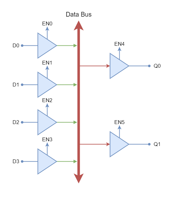
Using “Enable” lines of four data-in lines, any one of them can be connected to the data bus and its desired output (data-out) can be selected in a similar way. In this scheme, a total of six devices are connected to the common data bus and each of them can utilize this bus to route their data to different devices/ peripherals at the output.
Tri-state Buffer Control
The multiple Tri-state Buffers can be controlled using a digital decoder. The digital decoder, such as a Binary Decoder, has a number of binary inputs and selects the appropriate decoder output depending on the binary input signals. The Tri-state Buffers connected to that specific decoder output becomes active only whilst others remain at the “Hi-Z” state. Another state of binary inputs leads to a change in decoder output and another set of Tri-state Buffers interfaces the data bus. Meanwhile, other Tri-state Buffers become isolated. In the following figure, a 4-bit data bus is shown to be connected with four different data sets using a binary decoder.
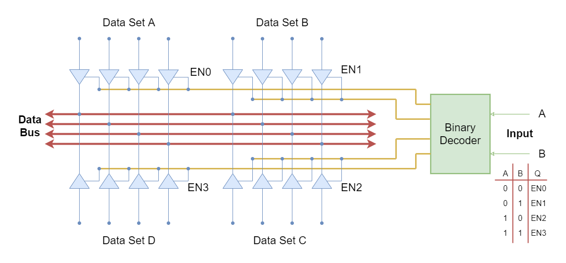
In the above figure, Data Set A gets connected to the common data bus when inputs are at state “00”. In the same way, Data Sets B, C, and D make an interface with the bus when inputs are at “01”, “10”, and “11” states, respectively.
Commercially Available Buffers
- CMOS based Buffers
- CD4050 Hex Non-inverting Buffer
- CD4503 Hex Tri-state Buffer
TTL based Buffers
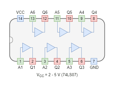
- 74LS07 Hex Non-inverting Buffer
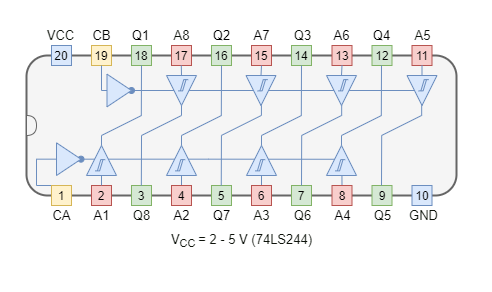
- 74LS244 Octal Buffer
In the following figures, a Digital Buffer (74LS07) and Octal Tri-state Buffer (74LS244) are shown.
Conclusion
- The Digital Buffer is a simple two-terminal device that is used for the amplification of digital signals.
- The Digital Buffer isolates the input and output circuits so that their impedances do not affect each other.
- The Digital Buffer can be non-inverting or inverting and, in the case of inverting, an inverted signal of input appears at the output.
- The Digital Buffers have high “fan-out” and “fan-in” capability which means that a number of devices can be connected at the input and output. Because of the high “fan-out” (current source) rating, a high current LED, switch, or relay can be driven through it.
- The Tri-state Buffer has an additional input terminal called “Enable” and a high impedance state “Hi-Z” compared to the Digital Buffer.
- The Tri-state Buffer output can be controlled through the “Enable” line leading to coupling and decoupling of input and output circuits. In disable or decouple state, a high impedance state (Hi-Z) appears between input and output terminals of the Tri-state Buffer.
- The Tri-state Buffers are commercially available in Active “HIGH” Non-inverting, Active “LOW” Non-inverting, Active “HIGH” Inverting, and Active “LOW” Inverting variants.
- The Tri-state Buffers are used in microprocessors or digital circuits to control the interfaces of data buses between devices.
- The Tri-state Buffers control can be driven using a Decoder which enables or disables a set of Tri-state Buffers depending upon the decoder output.


