OPAMP Monostable
Introduction As we have seen in previous tutorials, circuits can be categorized by the number of states that they can be stable. For example, in the op-amp multivibrator tutorial there were astable, monostable, and bistable versions of the circuit.
Introduction
As we have seen in previous tutorials, circuits can be categorized by the number of states that they can be stable. For example, in the op-amp multivibrator tutorial there were astable, monostable, and bistable versions of the circuit. This tutorial will focus on the monostable form of the circuit, specifically the implementation for an op-amp.
A monostable circuit is simply a type of circuit that has a single state that is stable. In most cases, this takes the form of a circuit that takes a trigger pulse of any length and outputs a pulse of a set length. The output pulse length is purely decided by the components that make up the circuit, and not the input pulse. So for example, if we have a monostable circuit with a time constant of 1ms, it would not matter if a 1us pulse or a 0.1ms pulse triggers it, the output pulse would always be 1ms long. Many different components could be used to make such a circuit, such as transistors, 555 timers, and digital logic gates, but in this tutorial, we will focus on the monostable op-amp circuit.
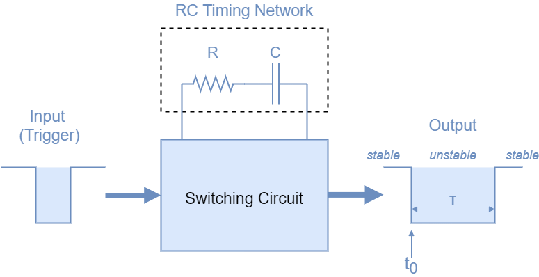
As you can see in figure 1, a monostable multivibrator is based around a resistor (R) and capacitor (C) circuit. These RC circuits are common in electronics and have a designated Greek letter Tau – τ to show this is a time constant. Changing the resistor and capacitor values will affect the time constant of the circuit.
Previous Circuit Recap
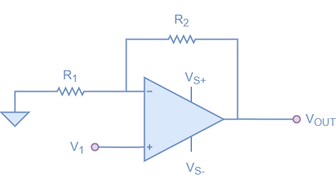
Similar to the multivibrator tutorial, the monostable op-amp circuit is based around a Schmitt comparator. To revise how a Schmitt comparator functions, it is set up similarly to an inverting op-amp, but instead of the resistor divider feeding back into the negative input, it is fed back into the positive. This provides a form of hysteresis, where the threshold changes depending on which state it is in.
The op-amp Schmitt comparator can be seen as a bistable circuit, as it has two stable states, with Vout only being stable at Vs+ or Vs-. The hysteresis is defined by the resistor network but has the opposite effect to the inverting op-amp. Instead of the op-amp output forcing the op-amp inputs together, in this configuration, it continues to amplify until it hits the supply rail. So when Vout is saturated towards Vs+ supply rail, the voltage at the positive input is positive with respect to ground. Similarly, when Vout is saturated to Vs- supply rail, the voltage at the positive input is negative with respect to ground. As with all resistor feedback networks, it uses the feedback equation shown below, and this feedback value has an impact on how the hysteresis functions, and defines the point that the input needs to reach for the comparator to switch.
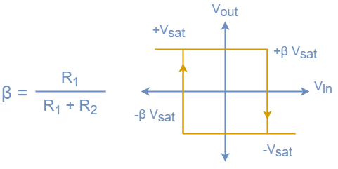
Note that with the above circuit, it is a bad idea to have very low values for hysteresis, as it will likely cause instability and unexpected switching. A similar circuit is used all of the time for inputs to microcontrollers, logic, and CPU’s. If you want to experiment with the circuit at home, you can always use a potentiometer in place of the two resistors, so you can change the feedback point, but it is a good idea to put it in series with a fixed resistor to stop the switching characteristic.
Basic Monostable Op-amp Circuit
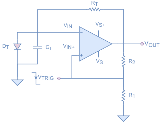
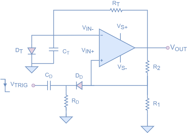
Figure 5 shows the basic monostable op-amp circuit, which we will use to describe the functionality and how it works. The circuit is controlled by a single input Vtrig and has a single output Vout and just a single active component, the op-amp.
For the setup above, with the diode in that direction, the stable state for the circuit is for Vout to be positive (Vsat+). Even with no input on Vtrig, Vout will likely swing high (after some instability). At that point, the feedback of R1 and R2, will create a potential of Vsat+*β where β is the feedback fraction described above. With Vout being forced to Vsat+, Vin- experiences a positive voltage, which is being clamped to 0.7V due to the diode being in the conducting direction (0.7V is the forward voltage of a standard diode). With Vin- being 0.7V, it is much lower than Vin+, which is why Vout is forced high. At this point, the capacitor in parallel with the diode is charging to 0.7V potential. At this point the circuit is stable.
If at this point a negative voltage pulse is applied to Vtrig, Vin– at 0.7V is higher than the negative pulse at Vin+. As we saw with the Schmitt comparator, this switches the state of the circuit. This different state forces Vout negative to Vsat-. If we assume the pulse is very short (we can deal with this in the next session) the voltage at Vin+ is Vsat-*β. At the same time, Ct now experiences a negative voltage (via Rt) which is not being clamped by the diode. This voltage causes the capacitor to start charging via Rt down to Vsat-. The capacitor Ct will continue to charge towards Vsat- until it reaches the same potential as Vin+, which is being set by the feedback resistors, meaning Vin+ is Vsat-*β. When the capacitor reaches this value, the Schmitt comparator switches the state back to Vsat+, its original state. The process then reverts to its original state, with the capacitor charging back to 0.7V.
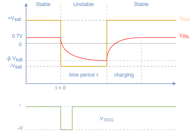
Some things should be noted about the above circuit that should be considered when designing it into your own circuitry. The capacitor Ct needs to recharge after the circuit returns to its stable state. This charging is through the same feedback resistor that it discharges through Rt. The other consideration is that the input pulse in Vtrig is assumed to be shorter than the time period of the charging part of the circuit. If this was not the case, and the pulse was longer, the circuit would remain unstable until the pulse returned positive.
Calculations
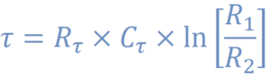
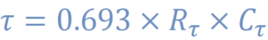
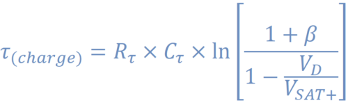
Figure 7 shows the equation used to calculate the time constant in the monostable op-amp circuit shown above, but to make it simpler, most engineers will use the same value for R1 and R2. This also makes the calculation simpler, producing the equation shown in figure 8. Now using this equation, the RC constant is directly proportional to the time constant, which makes the design simpler and easier to modify.
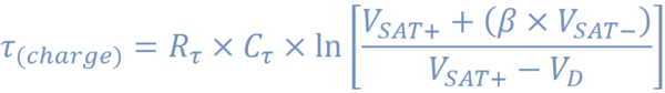
We can also calculate the time that it takes for the capacitor to charge from the switching point (Vsat-*β) and Vd (~0.7V). In this time where the circuit is recharging, it is important that a signal coming in is not expecting to make another pulse. So when programming into your circuit the minimum wait time, we can use the more complex equation shown in figure 9. In most cases, it is safer to just add a safe time, and not go through using the equation, but if your application requires fast pulses, you may need to optimize this time.
RC Differentiator Circuit
As discussed and shown above, this circuit will often need a particularly short pulse to trigger the mechanism, and depending on what is being used to trigger it, this pulse could have to be quite long (if you are using a microcontroller with a slow clock for instance), this is where the RC differentiator comes in. The basic form of this circuit utilizes the same RC phenomenon that the monostable op-amp uses to create the trigger, but this time in a slightly different format. Laid out similarly to a high pass filter, with a diode to only allow current in one direction.
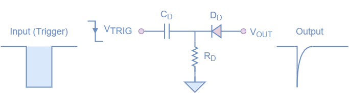
As we expect, the circuit triggers when the input goes from 0 to -Vs. At this point, the capacitor Cd begins to charge in the classic exponential capacitor charging curve. As the voltage across the capacitor is initially 0V, the output of the circuit immediately jumps to -Vs, which is seen as a spike on the output. As the capacitor charges, the output slowly returns back towards 0V in the classic capacitor curve. The diode is in a configuration where only a negative spike can pass through the circuit. If a positive trigger was applied, a spike would be produced by the capacitor, but blocked from the output by the diode.
There are some basic design rules that need to be considered when designing an RC differentiator like this. The first is to assume that the negative spike produced by the circuit will be less than or equal to the trigger voltage, which could impact a circuit that may need a larger spike. One other consideration is how to size the RC circuit. A well-followed rule, that should produce good quality spikes is to make sure the time constant τ is at least 10 times smaller than the expected input pulse width. If we use the calculation 5*Rd*Cd as the equation, if we had a pulse of 100ms, the outcome of 5RC should be less than 20ms (but closer to 10ms is better).
If we add the RC differentiator to the monostable op-amp circuit, we get the circuit shown in figure 11.
Conclusion
As we have seen in this article, an op-amp can be usefully used as a monostable circuit, and it can be modified to make longer or shorter pulses based on the resistors and capacitors chosen. This is a useful circuit, and monostable circuits can be very useful in modern electronics. Equally, almost any op-amp can be used, making the circuit universal. When designing, keep in mind that this exact behavior can be found by using other common components, such as 555 timers. Depending on what you need to achieve in your circuit will define which part you use.


