SkyWater and Google will use $15m Funding to expand an open source chip design project
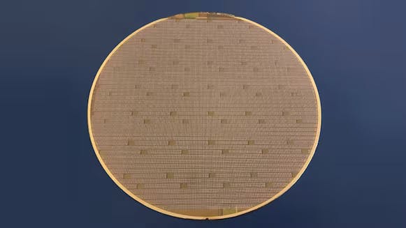
SkyWater Technology has announced that it will be extending its partnership with Alphabet’s Google, releasing an open source Process Design Kit., for its commercial 90nm, fully depleted silicon on insulator (FDSOI), CMOS process technology. This announcement came shortly after the US chip manufacturer received $15 million in funding from the US Department of Defense (DOD).
SkyWater Technology has announced that it will be extending its partnership with Alphabet’s Google, releasing an open source Process Design Kit., for its commercial 90nm, fully depleted silicon on insulator (FDSOI), CMOS process technology. This announcement came shortly after the US chip manufacturer received $15 million in funding from the US Department of Defense (DOD).
“Through this important investment from the DOD and collaboration with Google, we will enable open source design for our commercial SKY90-FD process technology, creating an IP [Intellectual Property] pipeline and pathway to commercial volume manufacturing,” says SkyWater CEO, Thomas Sonderman. “This will expand our 90nm foundry offering as a platform for innovation and productization here in the U.S.”
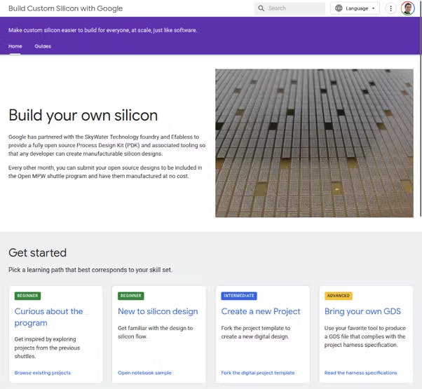
This is not the first time the duo will be partnering on a project like this; they joined forces together about two years ago to enable the open source design of custom application-specific integrated circuits (ASICs) on SkyWater’s 130 nm mixed-signal CMOS process node. The results of the project so far have been incredible as about 240 designs from the over 364 community submissions have been manufactured.
Speaking on why the US government decided to invest in the initiative, Thomas Sonderman stated that there’s a lot the government stands to get from the output of the development. The US military will have a new way to procure homemade chips in the future.
“We’re hoping that the collaboration is going to address what are really historical limitations of chip design and production, both for national defense as well as commercial markets, because researchers get improved accessibility and developers get to go through that exploration faster and candidly at lower costs,” said Google Public Sector CEO, Will Grannis.
The new platform is for analog-digital mixed-signal chips that we usually see in smart home products. This kind of chip takes advantage of larger transistors for cheaper production.
The partnership among the three represents a new era in accessible chip design driven by an open source approach. According to Matthew Kay, head of the new open-source silicon program at the Department of Defense,
“investments in commercial endeavors such as the partnership between SkyWalker and Google is another example of how the DOD can leverage technology advancement within the open source community to effectively and efficiently improve its defensive posture for the future.”
SkyWater provides the next-generation chip design system and secure fabrication facilities, Google provides the compute and technical know-how, while the $15 million funding from the Department of Defense makes it all scalable and accessible.
The process design kit, a set of files that describe the building blocks of the project, is open source but the fabrication process itself isn’t. Other useful details on this announcement are available on SkyWalker’s page and Google OpenSource Blog.


