Digital Logic Gates Summary
Digital Logic Gates Summary The digital logic gates are the main building blocks of any digital circuit either it is in the discrete component form or an integrated package. The logic gates can be constructed using resistors, diodes, and transistors such Resistor-Transistor Logic (RTL), Diode-Transistor Logic (DTL), and Transistor-Transistor Logic (TTL).
Digital Logic Gates Summary
The digital logic gates are the main building blocks of any digital circuit either it is in the discrete component form or an integrated package. The logic gates can be constructed using resistors, diodes, and transistors such Resistor-Transistor Logic (RTL), Diode-Transistor Logic (DTL), and Transistor-Transistor Logic (TTL). Amongst these, the Transistor-Transistor Logic (TTL) offers less propagation delay and low power dissipation. The Complementary Metal Oxide Semiconductor (CMOS) uses low-power MOSFET transistor logic enabling faster operation and high-power efficiency.
As discussed in previous articles, the three basic logic gates are “AND“,” OR“, and “NOT“. They perform basic multiplication (AND), addition (OR), and complement (NOT) functions. The “NOT” gate at the output of “OR” and “AND” gates form the logic “NOR” and “NAND”, respectively. They output the complement of the original function performed by “OR” and “AND” gates. Moreover, “NOR” and “NAND” gates are classified as “Universal Gates” because basic logics i.e. “AND”, “OR”, and “NOT” can be built using either NOR or NAND gates only. The logic gates, discussed above, can be used to make a combinational logic circuit, and cascading them can also lead to having more than one input.
Further to the above logic gates, the exclusive-OR (XOR) and exclusive-NOR (XNOR) logics perform arithmetic operations and calculations such as in Adders. They are complex in construction compared to the basic logic gates. Finally, the simple Buffers and Tri-state Buffers do not perform any logic yet they are an essential part of any digital circuit. They are used in the amplification of signals besides isolation of the input and output circuits. Whereas, the Tri-state Buffers give control over isolation which makes them suitable in digital circuits for interfacing of buses with the devices/ logic gates.
A brief summary of the aforementioned logic gates is presented below:
The Logic AND Gate
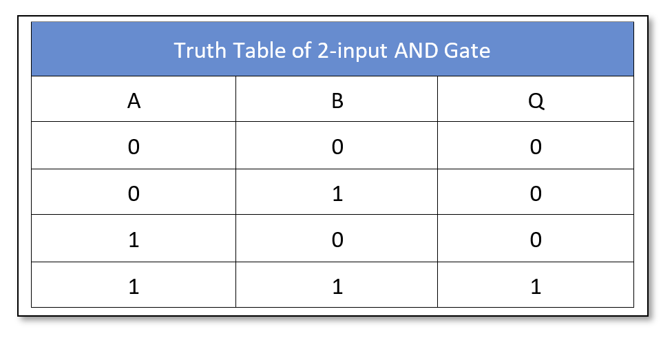
The logic “AND” gate symbol and truth table is shown below:

The logic “AND” gate is available in the following commonly used commercial packages:
CMOS based AND Gate IC Package
- CD4081 Quad 2-input
- CD4073 Triple 3-input
- CD4082 Dual 4-inputs
TTL based AND Gate IC Package
- 74LS08 Quad 2-input
- 74LS11 Triple 3-input
- 74LS21 Dual 4-input
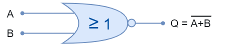
The Logic OR Gate
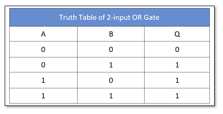
The logic “OR” gate symbol and truth table is shown below:

The logic “OR” gate is available in the following commonly used commercial packages:
CMOS based OR Gate IC Package
- CD4071 Quad 2-input
- CD4075 Triple 3-input
- CD4072 Dual 4-inputs
TTL based OR Gate IC Package
- 74LS32 Quad 2-input
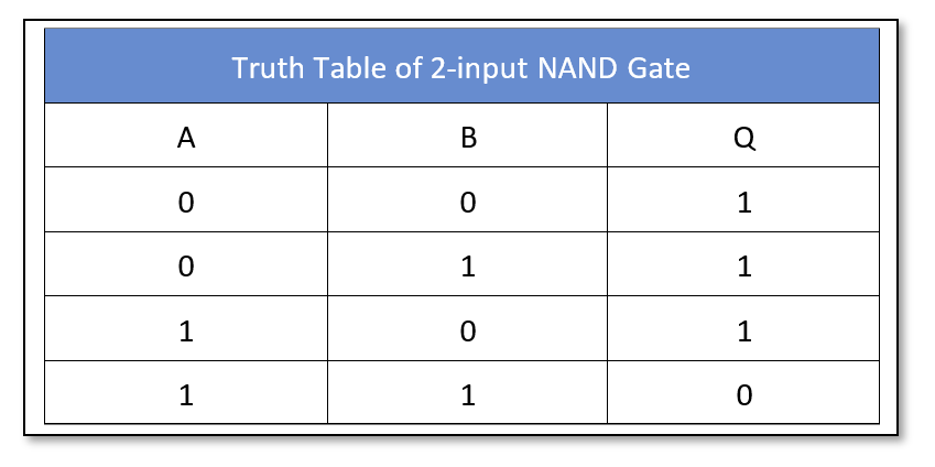
The Logic NAND Gate
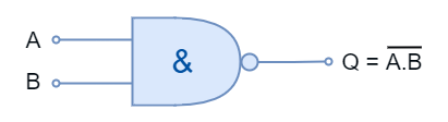
The logic “NAND” gate symbol and truth table is shown below:
The logic “NAND” gate is available in the following commonly used commercial packages:
CMOS based NAND Gate IC Package
- CD4011 Quad 2-input
- CD4023 Triple 3-input
- CD4012 Dual 4-inputs
TTL based NAND Gate IC Package
- 74LS00 Quad 2-input
- 74LS10 Triple 3-input
- 74LS20 Dual 4-input
- 74LS30 Single 8-input
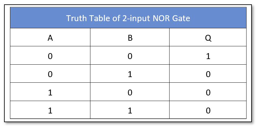
The Logic NOR Gate
The logic “NOR” gate symbol and truth table is shown below:
The logic “NOR” gate is available in the following commonly used commercial packages:
CMOS based NOR Gate IC Package
- CD4001 Quad 2-input
- CD4025 Triple 3-input
- CD4002 Dual 4-inputs
TTL based NOR Gate IC Package
- 74LS02 Quad 2-input
- 74LS27 Triple 3-input
- 74LS260 Dual 4-input
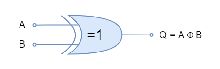
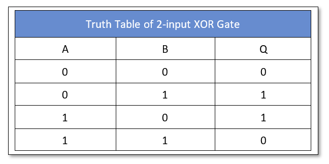
The Logic Exclusive OR (XOR) Gate
The logic “XOR” gate symbol and truth table is shown below:
The logic “XOR” gate is available in the following commonly used commercial packages:
CMOS based XOR Gate IC Package
- CD4030B Quad 2-input
TTL based XOR Gate IC Package
- 74LS86 Quad 2-input
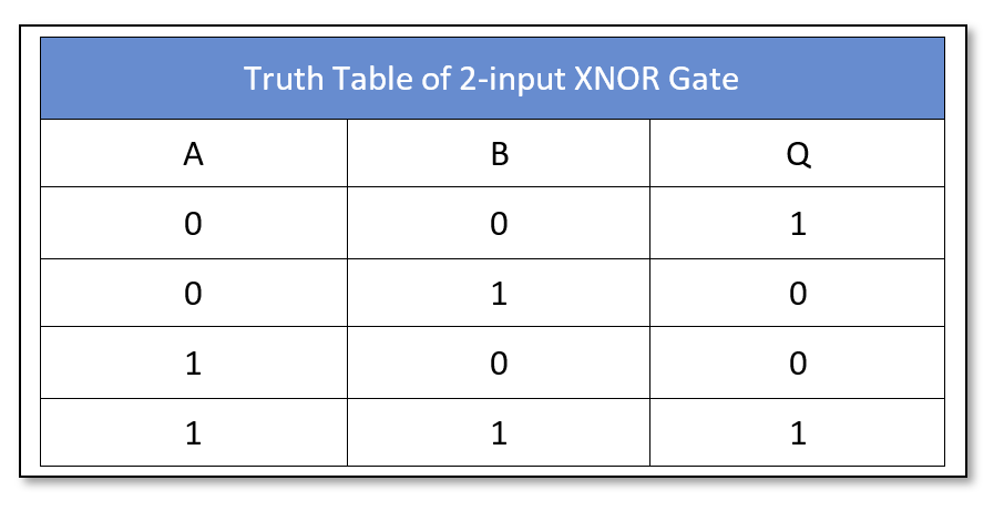
The Logic Exclusive NOR (XNOR) Gate
The logic “XNOR” gate symbol and truth table is shown below:

The logic “XNOR” gate is available in the following commonly used commercial packages:
CMOS based XNOR Gate IC Package
- CD4077 Quad 2-input
TTL based XNOR Gate IC Package
- 74LS266 Quad 2-input
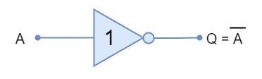
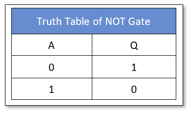
The Logic NOT Gate
The logic “NOT” gate symbol and truth table is shown below:
The logic “NOT” gate is available in the following commonly used commercial packages:
CMOS based NOT Gate IC Package
- CD4009 Hex Inverter
- CD4069 Hex Inverter
TTL based NOT Gate IC Package
- 74LS04 Hex inverter
- 74LS1004 Hex Inverter
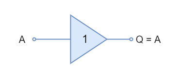
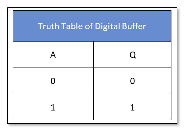
The Buffer
The Buffer gate symbol and truth table is shown below:
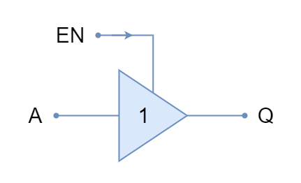
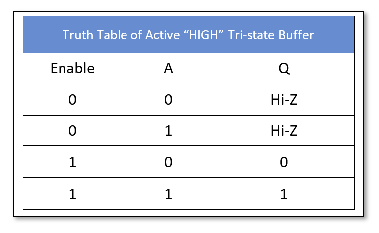
The Tri-state Buffer
The Tri-state Buffer gate symbol and truth table is shown below:
The Digital and Tri-state Buffers are available in the following commonly used commercial packages:
CMOS based Buffer Gate IC Package
- CMOS based Buffers
- CD4050 Hex Non-inverting Buffer
- CD4503 Hex Tri-state Buffer
TTL based Buffer Gate IC Package
- 74LS07 Hex Non-inverting Buffer
- 74LS244 Octal Buffer
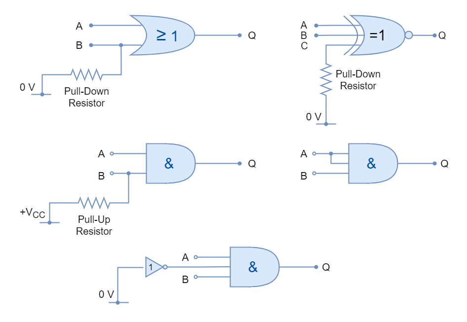
Pull-up and Pull-down Resistors
In using logic gates, it is essential to “Pull-up” or “Pull-down” any unused logic gate input depending on the type of logic gate function. It is required, particularly, in the logic gates having more than two inputs. Any floating input can lead to a false logic decision. Therefore, unused inputs of the logic gate require a pull-up or pull-down resistor. A suitable resistor such as 1kΩ or 10kΩ shall be used to connect to logic “HIGH” in case of pull-up and to logic “LOW” in case of the pull-down. The following figure illustrates the most common methods to connect unused inputs of logic gates.
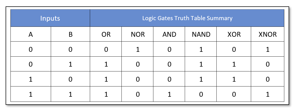
Digital Logic Gate Truth Table Summary
The truth table summary of the two input logic gates is shown below:
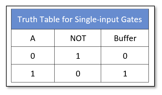
The truth table summary of the single input logic gates is shown below: