Combinational Logic Circuits
The digital logic circuit whose output, at any instant, is dependent on its inputs only, is referred to as a combinational logic circuit. The output state(s) of the combinational logic circuit is the logical result of the combination of its inputs and does not involve any kind of memory or storage, etc.
The digital logic circuit whose output, at any instant, is dependent on its inputs only, is referred to as a combinational logic circuit. The output state(s) of the combinational logic circuit is the logical result of the combination of its inputs and does not involve any kind of memory or storage, etc. Contrary to this, the output(s) of a sequential logic circuit is dependent on inputs and the previous state(s) of the output. The storage of the previous state of output acts as a memory in the sequential logic circuit, and feedback also plays a similar role.
The combinational logic circuit has no memory, storage, feedback, etc., which could affect its logical output besides inputs. At any instant of time, the states of inputs are immediately reflected at the output, depending on the logical combination of input states. This means that the output can change state from “0” to “1” or from “1” to “0” at the very moment the state of any input changes, accordingly.

Figure 1: The block diagram of a combinational logic circuit
Components of Combinational Logic Circuit
The combinational logic circuit consists of basic components such as logic gates, input, and output variables. The input and output variables represent digital states i.e. either “0” or “1”. Whereas, the logic gates form the combinational logic and may consist of NAND, NOR, and NOT logic gates. These logic gates are the basic building blocks of any digital logic circuit. The combination of two or more logic gates forms the combinational logic circuit. The NAND, and NOR logic gates, as discussed in the Logic Gates section, are termed “Universal Gates” as any other logical circuit can be constructed using only any of them. The combinational logic circuit can be simple or complex depending on the number of logic gates or logical operations it performs.
The task of a combinational logic circuit is to perform a defined logical function and there are multiple ways to specify a logical function. The function of a combinational logic circuit can be specified or expressed by the following methods:
Truth Table
The Truth Table represents the logical function of a combinational logic circuit in tabular form which lists all of the possible combinations of inputs and their states against the respective output(s). Simply, it lists the logical output(s) for each of the possible combinations of its inputs.
Boolean Algebra
The Boolean Algebra expresses the combinational logic in the form of an expression or equation. The expression relates the input and output variables to produce the desired function or output. The expression can be evaluated by feeding the input states i.e. “0”s and “1”s and checking for the outcome against the input states.
Logic Diagram
The logic diagram is the graphical representation of the combinational logic circuit. It consists of logic gates wired together in a specific manner to perform the desired function. The logic diagram details each and every logic gate used in the combinational logic by using a specific graphical symbol of each gate.
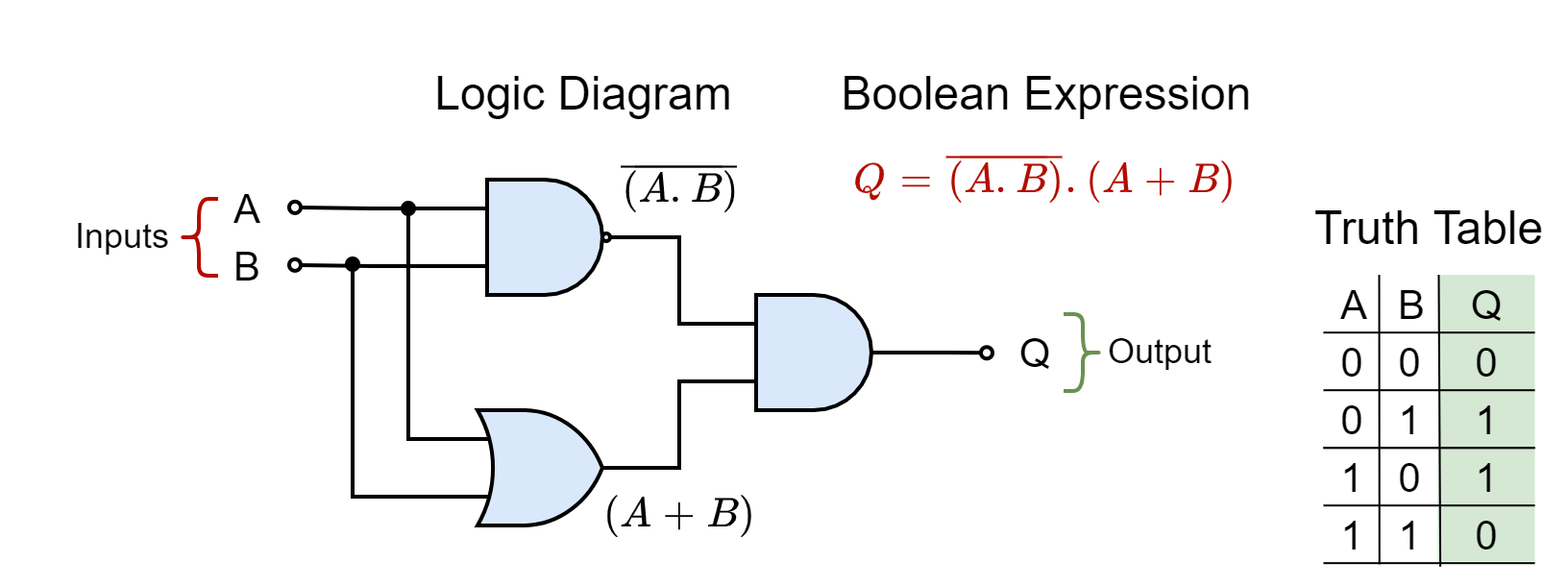
Figure 2: Three different methods for representing combinational logic
As said earlier, the combinational logic circuit consists of logic gates that are connected together in a combination to perform a specific function or decision, etc. The combinational logic circuit combines two or more input signals to produce at least a single output signal depending upon the logical operation it performs. The typical applications or functions performed by combinational logic circuits are Encoders, Decoders, Multiplexers, De-multiplexers, Adders, etc.
Classification of Combinational Logic
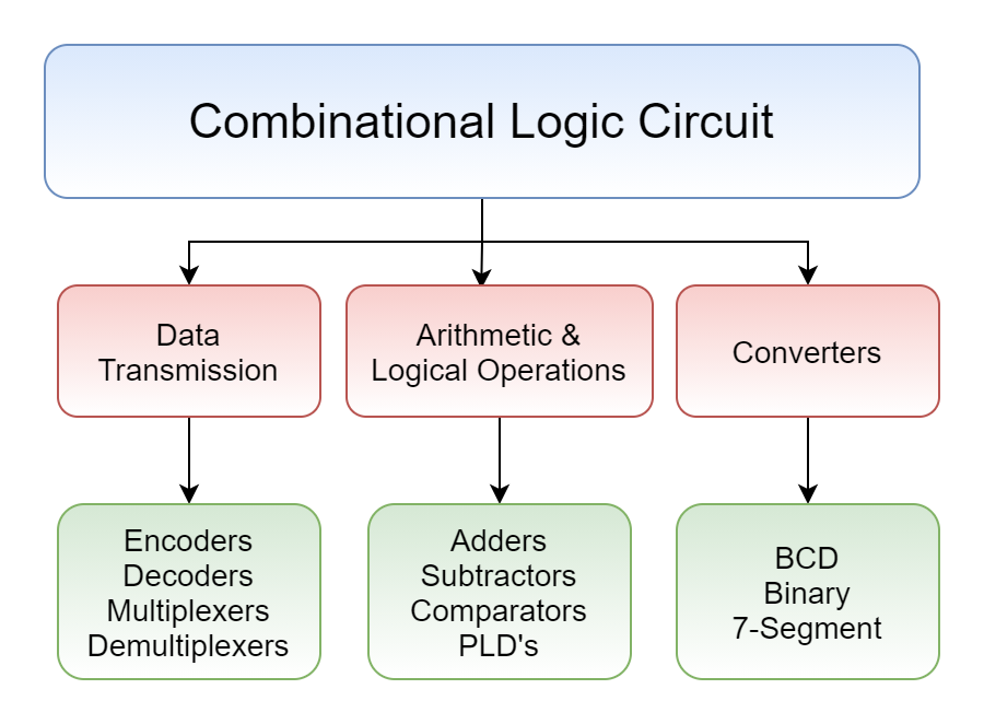
Figure 3: Applications of combinational logic circuits
Amongst the applications of combinational logic, the most important and widely used ones are multiplexer and de-multiplexer circuits. The multiplexers depending on the select lines, route one of the many inputs to a single output line. The select lines represent the code to select the input line which will be routed to the single output. As such, the select lines are decoded to identify the input to be routed. On the other hand, the de-multiplexer performs the reverse of the multiplexing, that is, it routes a single input to one of the many output lines depending on the select lines. The multiplexer consists of essentially two parts: decoder and solid-state switches. The application and working of the solid-state switches are described before discussing multiplexing, de-multiplexing, encoding, decoding, etc.
Solid-State Switches
Conventional electro-mechanical switches and relays are not used in digital systems mainly due to their high transition time. On the other hand, silicon-based solid-state switches have a fast transition time and they incur negligible losses. The Transistor-Transistor-Logic (TTL) based solid state switches use a transistor as a switch which is a unidirectional device. The field-effect-transistor (FET), Complementary-Metal-Oxide-Semiconductor (CMOS) based, devices act as bidirectional switches and are nearly perfect to be used in applications requiring bidirectional solid-state switches. The solid-state switches are commonly classified depending on the switching applications and have different types and ratings etc.
Applications of Solid-State Switches
The three (3) main switching applications of a solid-state switch are listed below:
- Analog Switches: They are used in routing signals such as audio, video, data switching/ communication, instrumentation and process signals, etc.
- Digital Switches: They are involved in high-speed signal routing, data transmission, and performing switching in digital peripherals such as USB, LAN, USART, Ethernet, etc.
- Power Switches: They are used in passing high voltage and current signals such as used in power supply modules, rectifiers, inverters, etc.
Analog Bilateral Switches
The analog bilateral switches are those which suppress (block) switching of data and signal currents when in the “OFF” state and allow the same when in the “ON” state only. The triggering of the switch state is carried out by a digital signal applied at the control gate of the switch. The switching, between “OFF” and “ON” and vice versa, is rapid. The switch offers a negligible resistance (ideally zero) in the “ON” state and very high resistance (ideally infinite) when it is “OFF”. In the following figure, a typical bidirectional solid-state switch consisting of N & P-channel MOSFETs is shown.
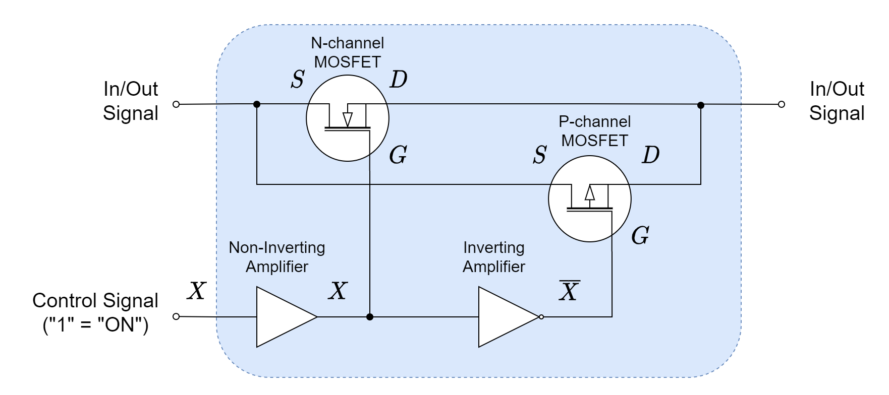
Figure 4: The typical diagram of bidirectional MOSFET-based switch.
The direction of signal or data can switch from left to right or from right to left depending on the states of MOSFETs and the voltage level of both sides. The states of MOSFETs are triggered by the “Control” signal. When the “Control” signal is “1” then N-channel MOSFET is “OFF” and P-channel MOSFET is “ON”. The states of MOSFETs are reversed when the “Control” signal is “0”.
Types of Contact
Just like electro-mechanical switches, the solid-state switches are also termed according to the number of throws and poles each switch offers. For example, Single Pole Single Throw (SPST), Single Pole Double Throw (SPDT), Single Pole Quad Throw (SPQT), etc. The state of each contact is either “Open” or “Closed” and under normal conditions i.e. unenergized state they are standardized as “Normally Open (NO)” and “Normally Closed (NC)”, respectively. Moreover, they also include configurations such as make-before-break and break-before-make, etc.
The following figure illustrates a few contact types.
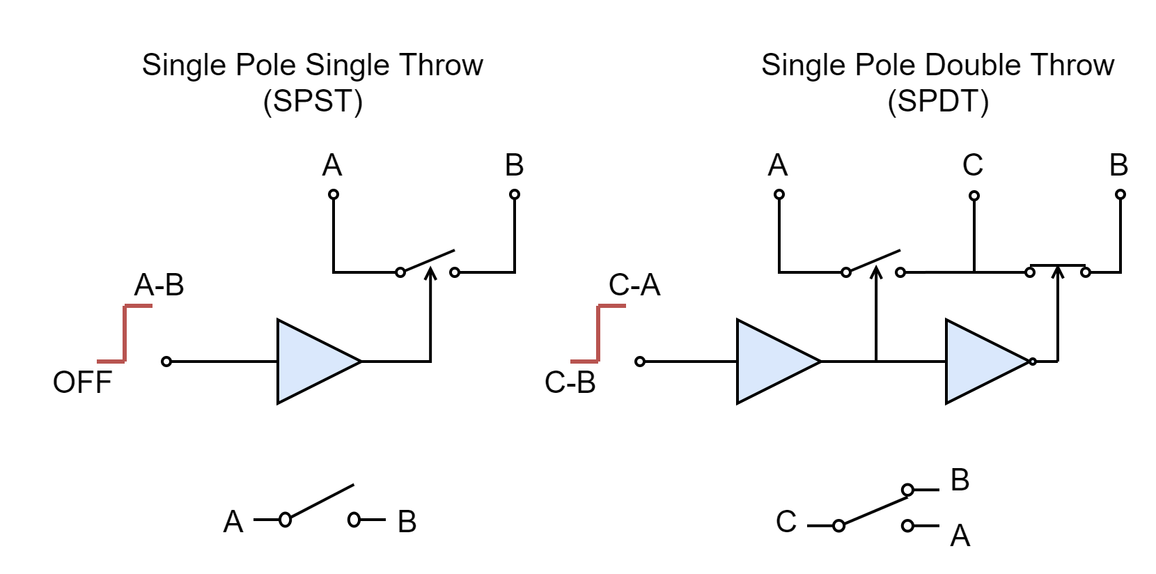
Figure 5: The Single-Pole-Singe-Throw (SPST) and Single-Pole-Double-Throw (SPDT)
The analog switches are commercially available in the form of IC packages and each IC includes multiple switches to form multi-channel multiplexers. For example, the 74HC4066 has four (4) independent bidirectional switches. The commonly known multiplexer and demultiplexer have Multi-way Bilateral Switches which are variants of CMOS analog switches.
Conclusion
- The digital circuit whose output is dependent on the combination of inputs only is called a combinational logic circuit.
- The combinational logic circuit has no “memory”, “timing”, or “feedback”. There is no storage or role of the previous state(s) of output(s) in the determination of the next output state(s).
- The output(s) of the combinational logic circuit changes in accordance with the inputs only, instantaneously.
- The combinational logic circuit performs the function which can be specified or expressed by a truth table, Boolean expression, or a logic diagram.
- The most common applications of combinational logic are multiplexers, demultiplexers, half adders, full adders, encoders, and decoders.


Wow this is great information I need to know about, thank you so much for the information.