Meet CH9102F, a Low-Cost Alternative to CP2104 USB-to-UART Bridge

As the applications of USB interfaces on computers, MCU boards, devices, and other I/O peripherals increases, there’s a parallel increase in demand for cost-effective and high-power USB bus converters for serial and parallel interfaces. CH9102F, a low-cost USB to high-speed serial port chip manufactured by Nanjing Qinheng Microelectronics, is one of such.

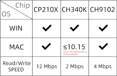
The CH9102F is a CH9102 family of USB to single serial port chips that features a full-duplex serial port, transceiver buffer, and a maximum baud rate of 4Mbps. The chip supports an operating voltage of 3.3 – 5V and serial port I/O interface signals of 1.8 – 5V range, as well as support RS232 and RS485 interfaces. The chip is also compatible with modem interface signals: CTS, DSR, RI, DCD, DTR and RTS, defined and controllable by computer/user application which makes it a versatile and flexible chop for professional and DIY projects.

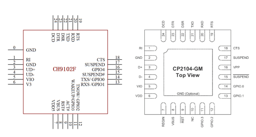
The CH9102F comes as a 4x4mm ultra-small square with 24 pins, supporting 485 direction control, a built-in crystal oscillator, built-in power-on reset, and a USB 2.0 interface. It features an EEPROM, configurable with chip VID, PID and other relevant parameters that can be seen on its datasheet. Going further, when compared to CP2104, apart from lower cost, the CH9102F has 6 GPIO pins while the former has 4 GPIOs with similar pin-outs. For makers, these extra pins make an advantage allowing for more peripheral expansion. This is a big reason it should be a favorite chip to makers, DIY users, and hobbyists alike.

image source: www.cnx-software.com

Features and Specifications

The features of the chip gotten from its datasheet are given below:

  • Power supply: 3.3 – 5V
  • A full-speed USB device interface, USB 2.0 compatible.
  • Serial port interface I/O powered independently, supports 5V, 3.3V, 2.5V, 1.8V power supply voltage.
  • A built-in firmware, which emulates a standard UART interface, is used to upgrade the original serial peripherals or expand additional serial UART via USB.
  • Its original serial applications are compatible without any modification.
  • It supports a free-installation operating system built-in CDC driver or multi-functional high-speed VCP manufacturer driver.
  • It has hardware full-duplex serial UART interface, integrated transmit-receive buffer, supports communication baud rate varies from 50bps to 4Mbps.
  • It supports 5, 6, 7 or 8 data bits, supports odd, even, blank, mark and no parity.
  • It supports common MODEM interface signals RTS, DTR, DCD, RI, DSR and CTS.
  • It supports CTS and RTS hardware automatic flow control.
  • Supports half-duplex, provides sending status TNOW supports RS485 switch.
  • Provides further RS232 interface, through external voltage conversion chip.
  • Built-in power-on reset, built-in clock, no external crystal required.
  • RoHS compliant QFN24

On the software part, the CH9102F runs on a high-speed virtual COM port (VCP) manufacturer’s driver or a free-installed OS built-in communication device class (CDC) driver. It supports CTS/RTS hardware flow control protocol to handle frame collisions during data transfer.

Applications:

  • To expand the UART interface of the computer and MCU.
  • To upgrade serial devices: MCUs to the USB bus.
  • USB to RS485 conversion.
  • USB to RS232 conversion.
  • USB to TTL serial port conversion.

CH9102F is available for purchase on 1688 for ¥5.50.

For further information and configurations, download the datasheet.

RealityCheck AD – Performing Anomaly Detection in the Right Way

RealityCheck AD by Reality AI

Reality AI recently announced RealityCheck AD at Sensors Converge Expo 2021 in partnership with Advantech. It provides advanced Anomaly Detection (AD) for equipment monitoring and end-of-line testing. It comes with Edge Node hardware from Advantech or RasPi, Reality AI Edge Node firmware, Reality AI Tools machine learning software, and several sensors to choose from.

Talking more from the software perspective, Reality AI combines advanced signal processing with Artificial Intelligence on inexpensive processors. To derive a custom transform depending on time and frequency, Reality AI employs an algorithmic search of a wide variety of feature spaces. Moreover, the code runs on ARM M- R- A-, and non-ARM microcontrollers, as well as on Intel processors and Linux

What is Anomaly Detection?

Anomaly detection refers to the detection of some abnormal data or information which is different from the normally expected data. Intrusion detection, fraud detection, fault detection, system health monitoring, event detection in sensor networks, identifying ecological changes, and defect identification in pictures using computer vision are all examples of anomaly detection. Anomaly detection is also important to monitoring the proper functioning of industrial equipment and conducting quality control inspections.

Anomaly Detection methods find a baseline normal region in a feature space using one of several different machine learning algorithms. Then scores are calculated for each observation that provides a measure of how “far away” that observation is from the normal baseline region in that feature space. The “farther away” that observation is, the less like normal it is. By applying a threshold to these scores, you can declare observations that are “too far from normal” to be anomalous.

2D Projection of Data
Sample 2D projection of multidimensional feature space, with observations that have anomalous and normal scores color-coded. Typically, normal points are clustered in a compact region, with multiple clusters of anomalies well separated, and a “fog” of anomalous points around the space

Performing AD in the right way

The wrong ways of doing anomaly detection include building AI models with very little or no data on known anomalies. For an efficient model, there must be a sufficient amount of anomalous data. If such kind of data is not available, a few anomalies can be created for testing.

Also, gathering and testing in limited and controlled circumstances must be avoided. Instead, data should be gathered and tested continuously in a wide range of conditions, while screening out false positive and false negative values as they can affect the efficiency of the model.

Moreover, some instruments can miss some important data that matters the most. Hence, using sophisticated sensors or instruments for gathering rich quality data is important. Also, try to include metadata wherever possible.

RealityCheck AD for Efficient and Easy Anomaly Detection

The RealityCheck AD offers a complete hardware and software solution for AI-driven, machine-level analytics for a factory or any product. It includes a self-learning edge node which is a rail mountable edge unit manufactured by Advantech. The RealityCheck AD Edge Node is based on the Advantech EPC-S201 embedded PC. It features an Intel Celeron N3350 Dual-Core SoC with 8GB RAM and 64GB SSD. It offers wi-fi, wired ethernet, and cellular connectivity.

RealityCheck AD Edge Node

Sensor options available for interfacing include:

  • Industrial-grade accelerometers – relatively high cost, but hardened with standard machine mounts and tight tolerances.
  • Lower-grade accelerometers – cheaper, with wider tolerances and lacking industrial hardening, but still sufficient for many tasks
  • Current and Temperature sensors
  • Contact Microphones – similar to an accelerometer, but with very high sample rates. Usually not available in industrial packaging, but still useful for many applications.
  • Free-standing microphones – for capturing ambient sounds and noise events.
  • Explosion-proof options are available.

RealityCheck AD also comes with Reality AI Tools® software for automatic generation of machine learning models for anomaly detection, signal processing & classification, and remaining useful-life predictions.

Key Features and Advantages of RealityCheck AD

  • The Edge Node learns “normal” automatically and starts detecting anomalies.
  • Edge Node can be taught “idle” so that unproductive equipment time can be tracked accurately
  • Any anomalies are shown on a dashboard and captured for future investigation, analysis, labeling, and use in model development. Over time, this data can be used to create detectors for specific conditions and to predict the remaining-useful-life of components.
  • Generates results in a short period, improving the results over time with feedback.
  • Easily integrates with Manufacturing Information Systems, dashboards, and workflow management systems using MQTT.

RealityCheck AD Architecture

Firstly, the data is gathered through various sensors like contact mic, accelerometer, temperature sensor, pressure sensor, etc. These sensors are interfaced with the Reality AI AD Edge Node that is based on the Advantech EPC-S201 embedded PC. This data is then processed by the Reality AI Tools software. It uses machine learning algorithms for creating classification, regression, correlation, and anomaly detection models, and deploying them to the edge.

Based on the baseline data, it quickly detects any abnormal observations. After detecting anomalous data, the edge node reports the status to the user via an illustrative and user-friendly dashboard. Also, the detected anomalies can be used for workflow integration by investigating the anomalous data and giving feedback to the model for improving its performance. Over time, it can perform more detailed detection of specific conditions and even predict anomalies before they occur. You can visit the official page of RealityCheck AD for detailed information.


Architecture of RealityCheck AD

Conclusion

The RealityCheck AD by Reality AI in partnership with Advantech provides a complete solution for industrial equipment monitoring and end-of-line testing. Numerous sensors integrated with the edge node gather data and start detecting anomalies based on the baseline data automatically. Moreover, it also provides a convenient and user-friendly API for integration with dashboard and workflow systems. It is a gamechanger in the field of industrial equipment monitoring and end-of-line testing.

RealityCheck AD solution will be showcased in the Sensors Converge event this month and Auto Tech Science Fair in October.  Consider registering for these events for similar hardware solutions.

STMicroelectronics Introduces 70 W Qi Compliant Chipsets for Ultrafast and Convenient Charging

STMicroelectronics’ STWLC98 integrated wireless power receiver delivers faster wireless charging and flexible charge sharing for diverse portable and mobile devices for home, office, industry, healthcare, and in-car applications. When combined with the STWBC2-HP transmitter IC, the complete transmitter-receiver system can deliver up to 70 W on the receiver end at high system efficiency.

The STWLC98 can fully charge today’s high-end smartphones, which contain high-capacity batteries, in just under 30 minutes. In addition, the new device extends opportunities for ultra-fast and convenient charging, free of cables, sockets, and restrictive connections, to a host of new applications and contexts. Moreover, contactless charging lets product creators simplify enclosure designs, reducing cost and complexity while encouraging new slimline styles and eliminating problems associated with the socket such as contamination.

Compliant with the Qi EPP 1.3 wireless-charging standard commonly used in the smartphone industry, the STWLC98 is managed by a 32-bit Arm Cortex-M3 core that supports a range of rich features including built-in protection; it comes with an embedded OS that simplifies Qi 1.3 standalone certification. On the transmitter side, the STWBC2-HP can work with ST’s STSAFE-A110 secure element to store official Qi Certificates and provides authentication that leverages state-of-the-art cryptography. Support for the Company’s innovative ST Super Charge (STSC) protocol enables fast-charging up to the maximum power transfer rate of 70 W.

The STWLC98 features ST’s proprietary Adaptive Rectifier Configuration (ARC) mode that enhances the ping-up and power transfer spatial freedom of the system in both horizontal and vertical directions without any change in hardware or coil optimization. Enabling ARC mode, which transforms the whole surface of the transmitter as a usable charging area, increases the ping-up distance by up to 50 % in all directions.

The STWLC98 works directly with the STWBC2-HP, which contains a USB-PD interface, digital buck/boost DC-DC converter, full-bridge inverter, three half-bridge drivers, and voltage, current, and phase sensors. Controlled by a Cortex-M0+ core, the STWBC2-HP executes a patented fast PID loop and also supports the STSC protocol.

ST’s new 70 W wireless-charging chipset creates a scalable solution that can be deployed in devices like smartphones, tablets, laptops, power banks, True Wireless Stereo (TWS) devices, Bluetooth speakers, and AR/VR headsets. Designers can also extend fast and convenient wireless charging to medical equipment like monitors and medicine pumps, as well as cordless power tools, mobile robots, drones, and e-bikes. The chipset is also suited to automotive applications including in-cabin charging solutions and wireless charging of various modules onboard the vehicle.

With built-in power management, the STWLC98 has an energy-saving ultra-low-power standby mode while total end-to-end charging system efficiency can exceed 90 %, thereby complying with stringent eco-design targets. The power charger chip features dedicated hardware and advanced algorithms that were developed to address challenges in ASK and FSK communication during high power delivery. Safety features include foreign object detection (FOD), which leverages high-accuracy current-sense IP, Q-factor detection, and robust communication between transmitter and receiver.

As an additional feature that gives users extra flexibility, the STWLC98 can also operate in high-efficiency transmitter mode to allow high-power charge sharing between devices. This is coupled with the STWLC98’s industry-first embedded Q-factor detection in a receiver device to ensure safe operation in transmitter mode.

Users of ST’s wireless power solutions can download and benefit from the free PC-based graphical tool, ST Wireless Power Studio, to accelerate design-in and simplify processes including calibrating FOD, tuning Q-factor detection, and communication diagnostics. Both devices are in high-volume mass production. The STWLC98 is packaged as a 4.3 x 3.9 x 0.4 mm 90-bump WLCSP and the STWBC2-HP is available in 8.0 x 8.0 x 0.4 mm VFQFPN-68 package.

more information: https://www.st.com/content/st_com/en/products/power-management/wireless-charger-ics/stwlc98.html

Broadcom ACFJ-3262 is a 10 A dual-channel gate drive optocoupler

The ACFJ-3262 is a 10 A dual-channel gate drive optocoupler device in the SO-24 package designed for high voltage, space-constrained industrial applications

The ACFJ-3262 is a 10 A dual-channel gate drive optocoupler device in the SO-24 package designed for high voltage, space-constrained industrial applications like motor drives and inverters. The new package features a 600 V CTI mold which reduces the creepage requirement due to high insulation voltage in a compact footprint. It features transient immunity (CMTI) greater than 100 kV/μs, preventing erroneous gate driver failures in noisy environments. The new device has less than 95 ns propagation delay, enabling high frequency switching to improve MOSFET and GaN transistor/FET driving efficiency

Key features

  • 10 A max peak output current
  • Dual-channel with 2.8 mm creepage between channels
  • 600 V CTI mold
  • Dual rail-to-rail outputs for separate source and sink

Additional features

  • Industry’s first 10 A gate drive optocouplers
  • 95 ns max propagation delay
  • 100 kV/µs minimum common mode rejection (CMR) at VCM = 1000 V
  • ICC = 4.0 mA max supply current
  • Wide operating VCC range: 10 to 25 V
  • 600 V CTI SO-24 package
  • Industrial temperature range:
    • From -40 to +125 °C
  • Safety approvals:
    • UL recognized: 5000 VRMS for 1 minute.
    • CSA approved
    • IEC/EN/DIN EN 60747-5-5 VIORM = 1.230 VPEAK

Applications

  • MOSFET and GaN transistor/FET gate drive
  • AC and brushless DC motor drives
  • Renewable energy inverters and storage
  • Industrial inverters
  • Switching Power Supplies (SMPS)

more information: https://www.broadcom.com/products/optocouplers/industrial-plastic/isolated-gate-drive-optocouplers/gate-drives/acfj-3262-000e

SparkFun AP63203 Buck/BabyBuck Regulator Breakouts

SparkFun AP63203 Buck/BabyBuck Regulator Breakouts are 2A synchronous buck converter boards that operate at 3.8V to 32V wide input voltage range. These breakouts integrate a 125mΩ high-side and a 68mΩ low-side power MOSFET that provides high-efficiency step-down DC/DC conversion. The AP63203 breakout regulators feature a proprietary gate driver design and Frequency Spread Spectrum (FSS) for Electromagnetic Interference (EMI) reduction. These regulator breakouts offer 0.8V ±1% of the reference voltage, 22µA ultralow quiescent current, and 3.3V output voltage. The Buck regulator is available in a 1-inch x 1-inch board and the BabyBuck regulator is available in a 0.4-inch x 0.5-inch board.

Features

  • Proprietary gate driver design for best EMI reduction
  • Frequency Spread Spectrum (FSS) to reduce EMI
  • Precision enable threshold to adjust UVLO
  • Totally lead-free and fully RoHS compliant
  • Halogen and antimony free
  • Protection circuitry:
    • Overvoltage protection
    • Cycle-by-Cycle peak current limit
    • Thermal shutdown

Specifications

  • 3.8V to 32V input voltage range
  • Upto 2A continuous output current
  • 0.8V ±1% reference voltage
  • 22µA ultralow quiescent current
  • 3.3V fixed output voltage

more information: https://www.sparkfun.com/products/18357

A Versatile Cellular-IoT Prototyping Platform with Self-powering Capabilities and Preloaded Global Data for Out of the Box Connectivity

Conexio Technologies are ready to launch their new IoT development kit powered by a Nordic nRF9160 system in package (SiP) which features an ARM cortex M33 application processor. The device can be used for building cellular-connected electronic projects such as asset tracking applications, smart wearables, smart farming, weather monitoring, smart meter monitoring, etc. It supports LTE-M, GPS, NB-IoT, and supports a global range of LTE bands.  The device also comes with 250 SMS and half a gigabyte of global data which is usable in over 100 countries with a validity of 10 years making it a fast and convenient tool to use right out of the box.

GPIOs and other Features for a Stand-alone Operation

The board features 26 mixed-signal user-programmable GPIOs for interfacing different sensors and actuators. The board has an inbuilt accelerometer, temperature, and humidity sensor apart from the GPS and cellular connectivity, it also features Energy Harvesting circuitry with MPPT functionality capable of recharging Li-ion or NiMH batteries by connecting up to 7 solar cells with the device making it a complete stand-alone package in itself. The pin-out diagram is given below.

The board also features 2 external U.FL antennas for GPS and LTE-M/NB-IoT connectivity, The external antenna makes it possible to weatherproof the device by enclosing it in a weatherproof box, only leaving the antennas outside. The stratus has a Micro-USB port for serial connectivity and 10 pin header for programming through J-Link and CMSIS-DAP. The OS on the board is Zephyr RTOS, and to make product development easier, Conexio has also developed an extension for Visual Studio Code and the company also promises to provide all the examples and VSC code extensions when the campaign starts in CrowdSupply.

The company also has an add-on Stratus shield for easing the interfacing of sensors and other peripherals with the Stratus module. The shield abates the need for soldering and reducing the number of wires required for interfacing sensors, actuators, or displays with the status. Thus, simplifying the connection process.

The features of the Conexio Shield are:

  • 1 x micro BUS: add-on board standard from Mikroe, allowing connection to over 800+ click boards.
  • 2 x Sparkfun Qwiic connector: SparkFun’s Qwiic Connect System, allowing to connect over 100+ Qwiic products.
  • 1 x Grove I2C connector: Grove is a modular, standardized connector prototyping system by Seeedstudio.
  • 1 x 2 Pin JST connector for plugging the solar panel input.
  • 1 x user-programmable LED
  • 3.3 V operating voltage

So, if you are interested in this board, you can check their website for more information. The project will soon go live on the Crowd Supply page and opt for notifications about the campaign

1-Cell Protection IC with Reset and Forced Standby Function for Li-Ion and Li-Polymer Batteries

Ricoh Electronic Devices has introduced a primary battery protection IC R5613 Series for rechargeable 1-cell Lithium-Ion and Lithium Polymer batteries. This Series is designed to enforce strict usage limits keeping the battery cell in optimal condition and preventing critical overload conditions. The new R5613 series features standard functions like over-charge and over-discharge voltage, discharge overcurrent, and charge overcurrent, and short circuit protection. The Target applications of this series include Li-Ion batteries or battery packs for portable devices such as smartphones, smartwatches, fitness trackers, or other electronic gadgets. Additionally, this IC features the RST pin function which can switch from an external MOSFET to either a RESET or a forced standby state.

The R5613 Series features a reset pin that enables controlling the IC externally and has two optional functions. This IC automatically enters the standby mode once the cell voltage drops below a certain threshold, some internal circuits will shut down, reducing current consumption and minimizing further discharge. It has a much lower current consumption (Typ. 2.0 – 2.5 µA) compared to predecessor products which are especially important for those applications with a small battery capacity. Moreover, the external current sense resistor value can be in the range of 1.5 mΩ which results in a lower heat dissipation at high currents.

Optional functions are available per product version, such as the 0 V battery charging, which offers the option to allow/disallow the battery to recharge from a deeply discharged state. Another option is to select between auto-release and latched release from overvoltage, Undervoltage, and discharge overcurrent status.

Application Circuit

Key Benefits of the R5613 Series:

  • Lower-resistance of Sense Resistor by Overcurrent Detector with Lower-voltage and High-accuracy: Achieving Heat Reduction on Board
  • Low Consumption Current and Low Standby Current: Achieving Longer Driving Time with A Battery of Small Capacity
  • Switching to RESET or Forced-standby State by RST Pin: Allowed External Control of Load

The R5613 Series IC is now available in an 8 pins DFN1616-8B package, measuring L1.6 x W1.6 x H0.4 mm. Samples and evaluation boards are also available from authorized local distribution channels and online partners.

more information: https://www.n-redc.co.jp/en/products/lithium-ion-battery-protection/spec/?product=r5613

Multi-Functional Programmable DC Electronic Loads Offer Multiple Operating Modes and High-Speed Response Times

The SFL series of 300W and 1,000W programmable electronic DC loads from TDK Corporation offer high-speed current control, eliminating load current overshoot and oscillation, low voltage operation, no turn-on delay, and linear operation from 0V.  The devices in the series offer 300W (3U high half-rack) and 1,000W (3U high full-rack) power levels and either a 120Vdc or 500Vdc maximum rating.

Each unit in the SFL series operates in 7 different load modes and 4 operating modes which enable customers to perform up to 17 different load tests on DC power supplies, fuel cells, solar cells, batteries, and components for optimal performance.

Loads of devices can be programmed for multiple load types, including constant current, constant resistance, constant power, external control, short circuit, and constant voltage with a current limit.  Additionally, the SFL load current rise and fall times (slew rate) can be controlled up to 30A/µs, and the internal memory can store and recall eight different load settings.

Key Features of the SFL Series

  • Stable High-Speed Current Control (No Dynamic Overshoot/Oscillation) with High Slew Rate (Up to 30A/us)
  • Low Voltage Operation with No Turn-On Delay
  • Seven Operating Modes (CC, CR, CP, CV, EXT, Short, CV+Climit)
  • Large 3.5″ Color LCD Screen
  • Load Terminals on Front and Rear Panel
  • Dynamic (Time / Frequency) Mode (Pulsating Load)
  • Sequence Operation (Waveform Generation)
  • Sweep Mode Test Function (V/I, OCP, OPP)
  • Built-In Memory Function (store/recall up to eight memory settings)
  • Parallel Operation (up to ten units)
  • Multi-Channel Triggering (up to ten units)
  • Built-In Protection & Alarms (Current Limit, Power Limit, OTP, OVP, Reverse Connection)
  • Optional IEEE (w/DIDO) Interface
  • Optional Ripple Measurement Interface

For higher power load requirements using a unit-to-unit RJ45 Ethernet cable, up to 10 units from the series may be paralleled in a master-slave arrangement. Besides, multiple SFL loads can be connected to separate devices using that cable for synchronized load control and dynamic operation. The SFL series can be programmed using analog or digital signals, with an optional ripple and noise measurement and IEEE interface.

more information: https://www.emea.lambda.tdk.com/uk/products/sfl

Russian Company Develops A Mikron Mik32 MCU With Features Similar To STM32l0 MCU

It’s no longer news that open-source RISC-V architecture has flung the door of innovation open for several companies to reinvent existing microcontrollers – a move that has become imminent, as countries around the world look forward to localizing their technologies and becoming more independent.

Russia has not lagged behind in this development and they have proven this with many of their inventions including the new Mikron MIK32 microcontroller.

Mikron MIK32 mimics the famous STMicro STM32L0 Cortex-M0+ MCU microcontroller, especially in its functionality, so much that they can be used interchangeably. Mikron MIK32 is a 32-bit RISC-V MCU with tons of input and output interfaces like UART, SPI, I2C, ADC and DAC, as well as an interrupt controller and several timers. The architecture of this microcontroller makes it suitable for several applications, such as gas/water meters, industrial sensors, and healthcare equipment – Potentially, lifecycle devices that utilize the famous STMicroelectronics’ STML0.

Let’s take a look at the specifications of the Mikron MIK32. You’ll love what it packs in for a comfortable sum of money!

  • CPU Core – 32-bit RISC-V up to 32 MHz with 32 registers,  embedded multiplier, debugger (TAP controller and JTAG interface), and interrupt controller
  • 256 bytes OTP ROM
  • 16KB RAM
  • 8KB EEPROM
  • Storage I/F: SPI, Dual-SPI, Quad-SPI interfaces for NOR and NAND flash devices
  • 4-channel DMA controller supporting low-power modes
  • 2x I2C, 2x UART with synchronous mode support, 2x SPI
  • 12-bit 8-channel ADC up to 1 MHz
  • 12-bit 2-channel DAC up to 1 MHz
  • 5V-tolerant digital I/O
  • 2x PVD (Programmable Voltage Detectors)
  • Clock control unit
  • Interrupt controller: Supports 32 interrupts from ADC, SPI, I2C, UART, timers, voltage detectors
  • 16-bit (3x) and 32-bit (2x) multifunctional timers supporting PWM, Capture/Compare; watchdog timer
  • Encryption: CRC calculation unit, Crypto accelerator with AES 128 support
  • RTC @ 32.768 KHz
  • Embedded temperature sensor
  • 3.3V +/- 10% input voltage
  • Power control unit supporting different power modes, power-down of main domain, and/or clocking of separate units
  • Break-out detector
  • Temperature Range: -40 – +85°C
  • Dimensions: 4.36 mm x 4.36 mm

What’s more?

Mikron also designed a Development Board with a MIK32 module, multiple relays, buttons, DIP configuration switches, and RS232/RS485. With this amazing product, you can support up to four expansion boards. This innovation makes Bluetooth, WiFi, GSM, NB-IoT, Zigbee, RFID, and/or Ethernet connections compatible with the board.

You can employ the Mikron MIK32 to use for water or gas meters, remote control, and user interfaces, industrial sensors, gaming, and GPS equipment, as well as PC peripherals.

With 450 roubles ($6) only, you can purchase the MIK32 RISC-V MCU, though I’m not yet sure if that is its unit price or price in quantities. You can contact the company to purchase the microcontroller or the development board.

You can also get more information from the official company website.

Arduino brings down the cost of the popular Portenta H7 board to Launch Portenta H7 Lite

Two years after Arduino launched the original Portenta H7 board, the first in a new family of products designed to take the brand into the realm of professional electronics design, the company is back with a new entry designed for fans of the Potenta H7 who may be working on a low-budget project and may not need some of the features.

According to the company, the Portenta H7 Lite (as it is aptly called) is “a streamlined, tightly targeted solution for AI applications and low-latency control projects.

” It is a cost-effective solution that offers top performance, reliability and versatility. If you don’t need all the features of the Potenta H7 board, then you can consider getting the Lite as it is specifically designed for “developers who want the computational power of Arduino Pro’s Portenta H7 flagship, but don’t need the video output, additional security features or connectivity.”

The Lite comes with almost all the other features that you would find in the original based Portenta H7 board: same STMicro STM32H747XI as its full-fat stable-mate, with an Arm Cortex-M7 core running at 480MHz and a Cortex-M4 core running at 240MHz, an on-chip GPU that makes it possible to build a dedicated embedded computer with a user interface as well as compatibility with all breakouts and shields built for the H7.

The differences however are in the radio connectivity, video output functionality, or a second secure element.

  • No support for DisplayPort via USB Type-C as well as MIPI DSI host and MIPI D-PHY capabilities)
  • Just one secure element, instead of two
  • Absence of the onboard Murata 1DX radio module which is supposed to simultaneously provide it with Wi-Fi 802.11b/g/n, Bluetooth 5.1 and Bluetooth LE connectivity (network connectivity is via Ethernet PHY accessible via the expansion port).

Dropping these features also brought down the cost of the Pro board, from $103.40 (Portenta H7) to $72 (Portenta H7 Lite).

The Portents H7 Lite is perfect for

“everything from high-end industrial machinery to laboratory equipment and mission-critical devices.”

Application areas include robotics controller systems and machine operations that don’t require a high-resolution video interface, as well as projects where security is important but not critical. You can also use it for crowded wireless applications that you can use an Ethernet connection for.

The Portenta H7 Lite is currently available and sells on Arduino Store at $72. Further details may also be found on the official website or announcement post.

TOP PCB Companies