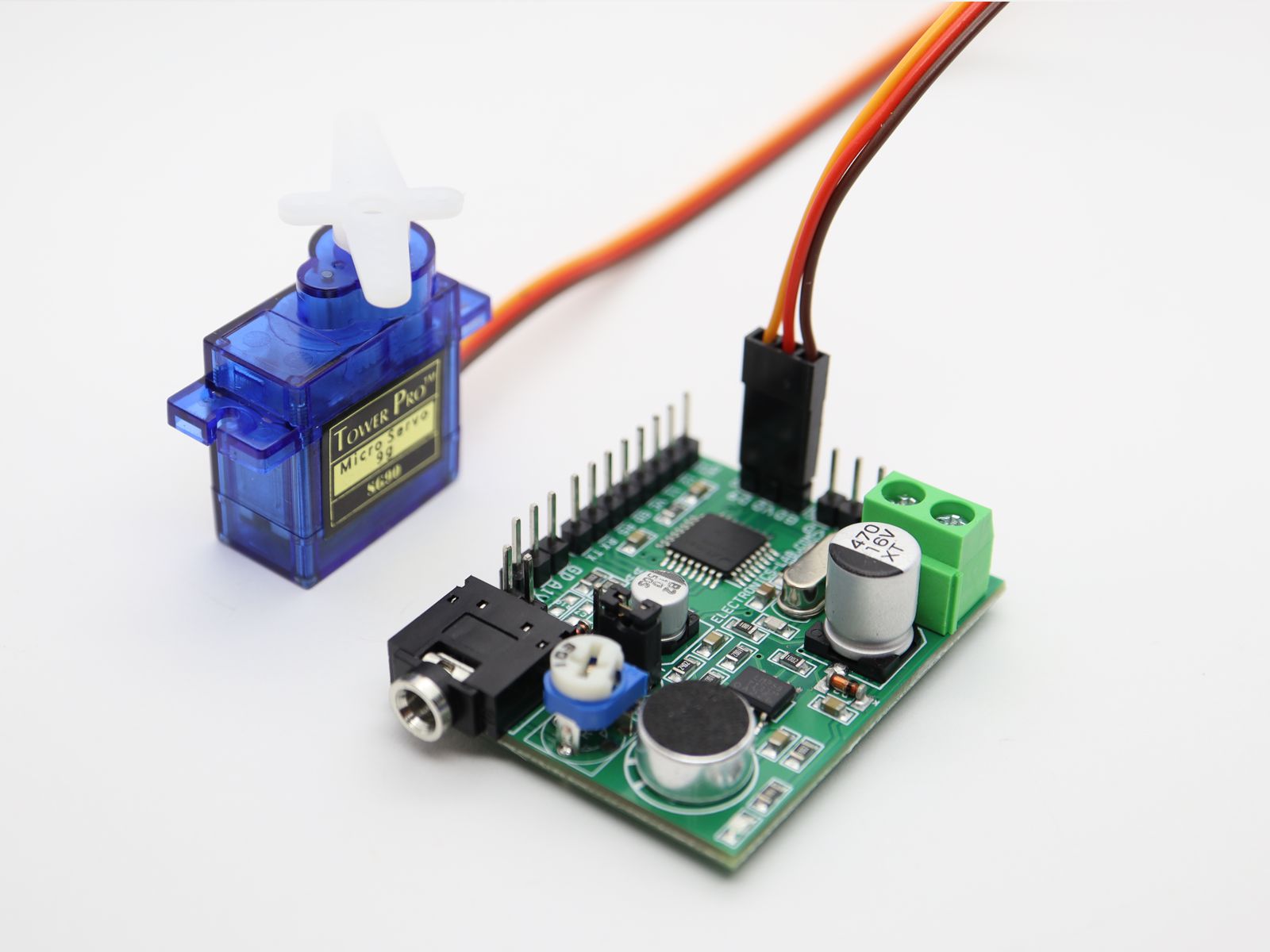
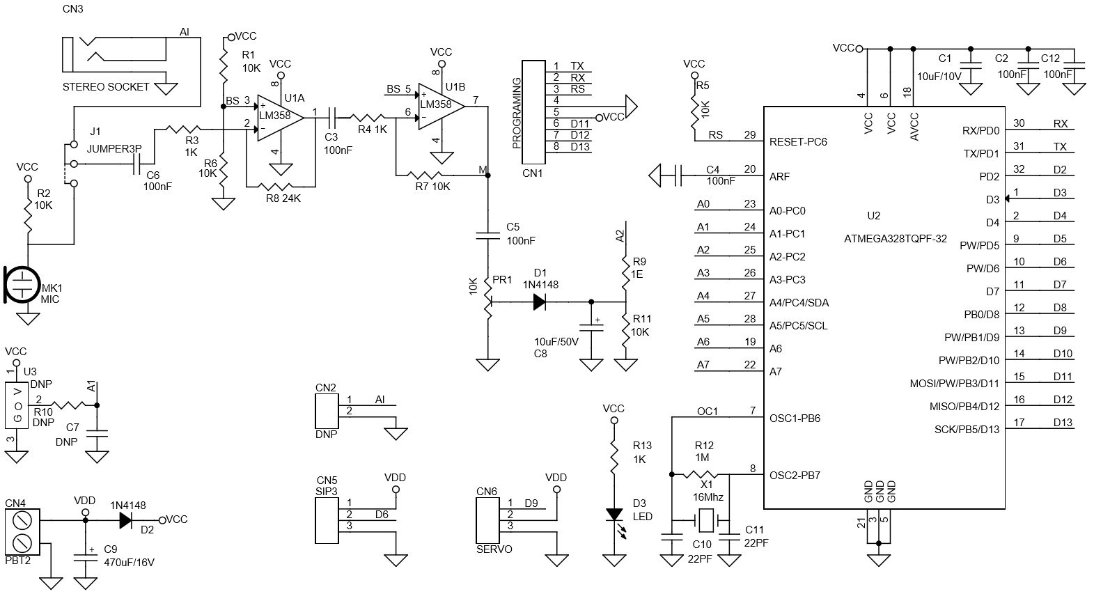
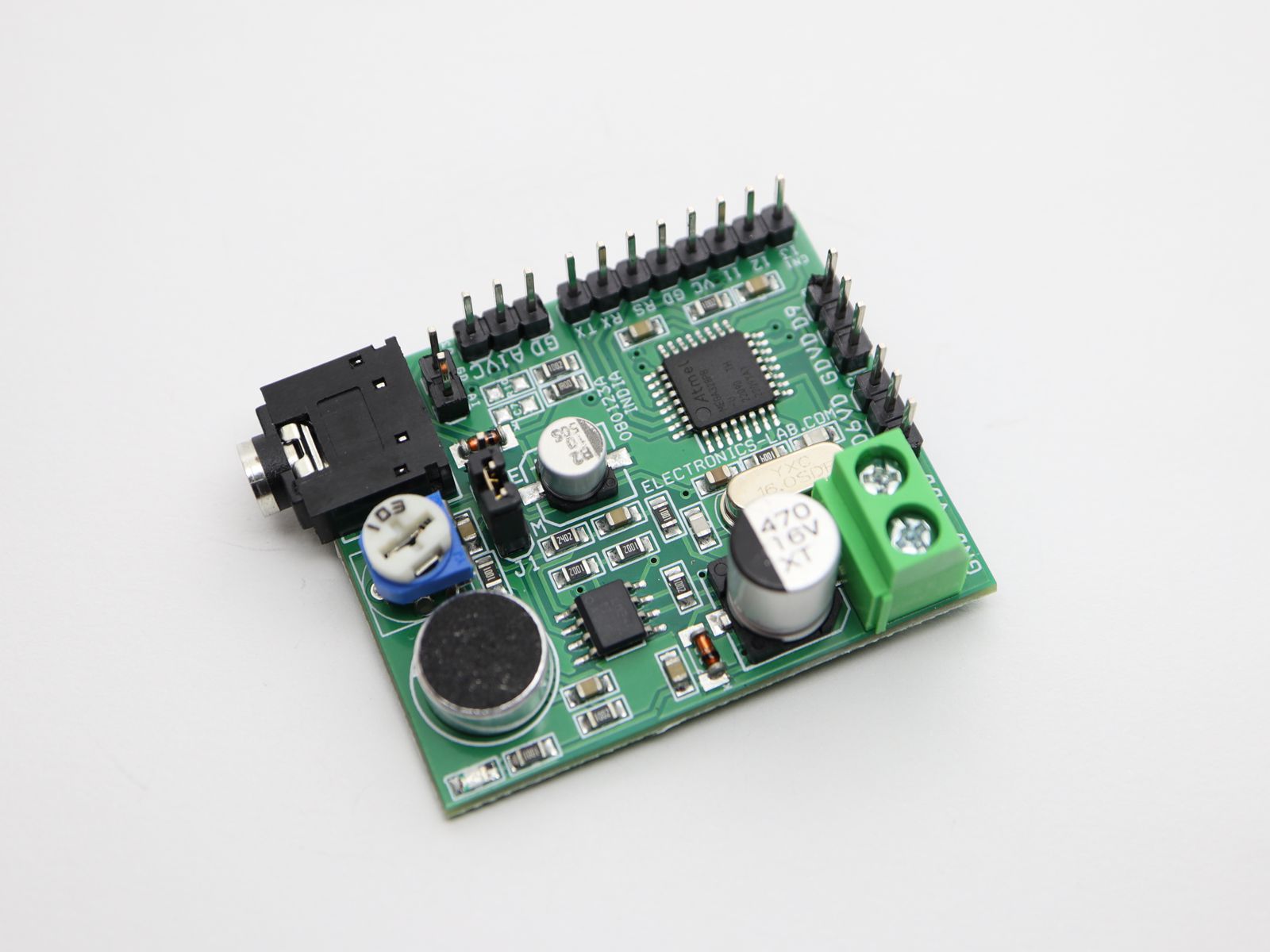
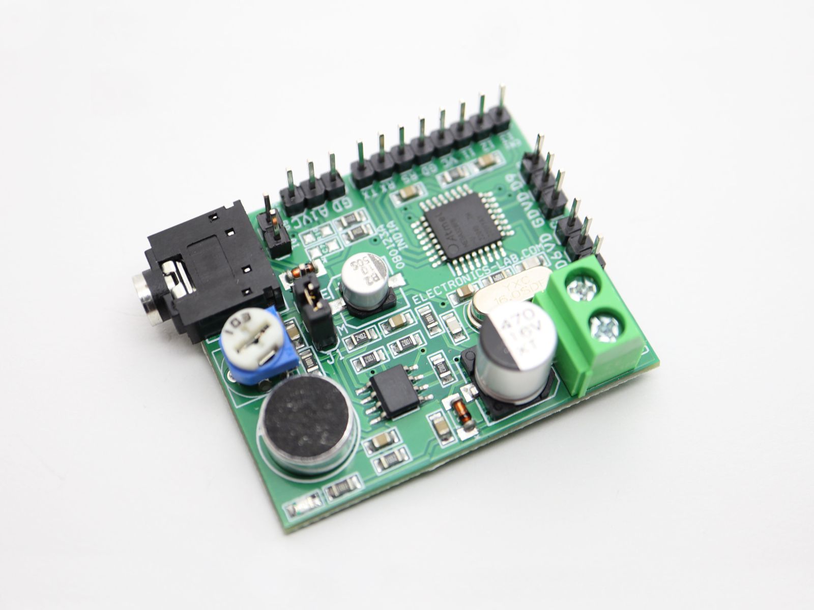
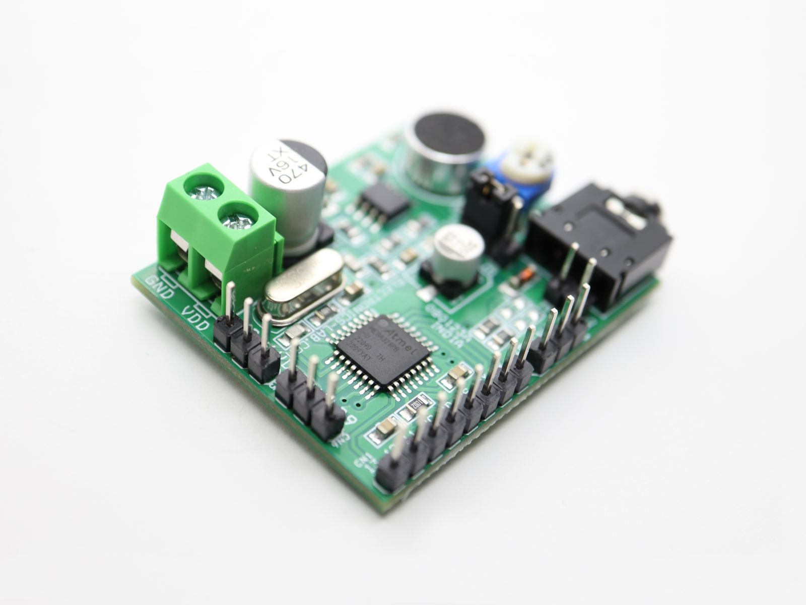
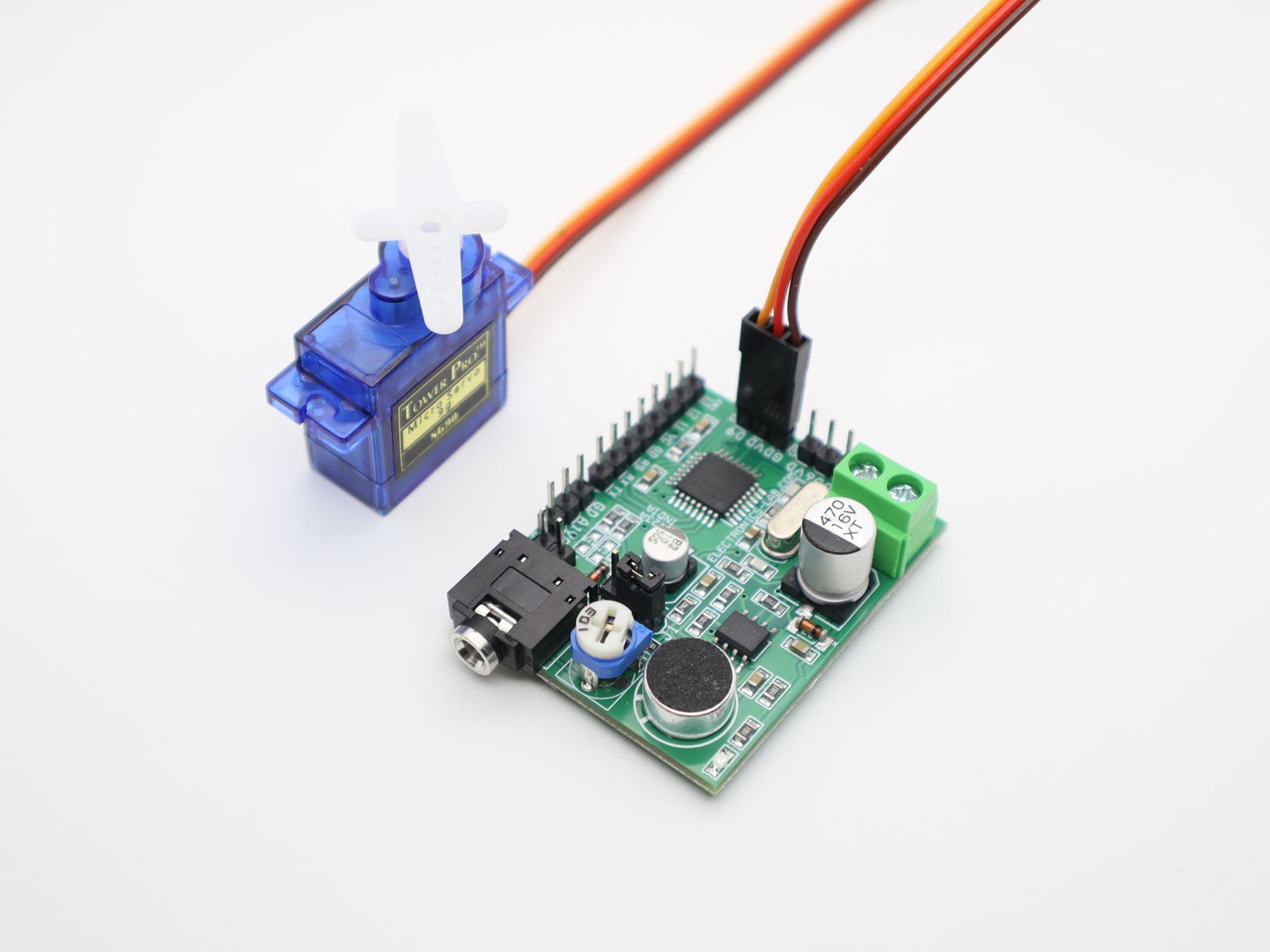
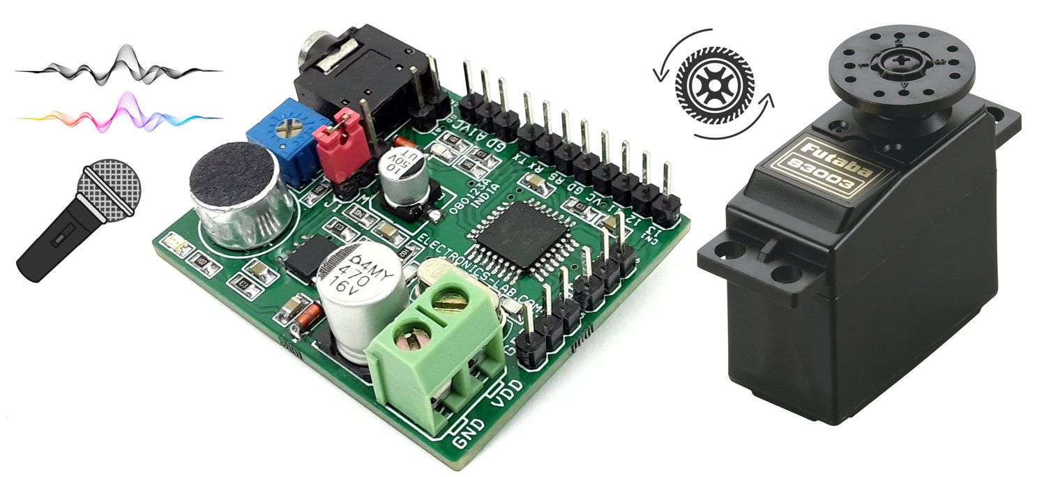
The project presented here is made for applications such as Animatronics, Puppeteer, sound-responsive toys, and robotics. The Arduino compatible board consists of LM358 OPAMP, ATMEGA328 microcontroller, microphone, and other components. The project moves the RC servo once receives any kind of sound. The rotation angle depends on the sound level, the higher the sound level the bigger the movement, in other words, the movement of the servo is proportional to the sound level. The microphone picks up the soundwave and converts it to an electrical signal, this signal is amplified by LM358 op-amp-based dual-stage amplifier, D1 helps to rectify the sinewave into DC, and C8 works as a filter capacitor that smooths the DC voltage. ATmega328 microcontroller converts this DC voltage into a suitable RC PWM signal.
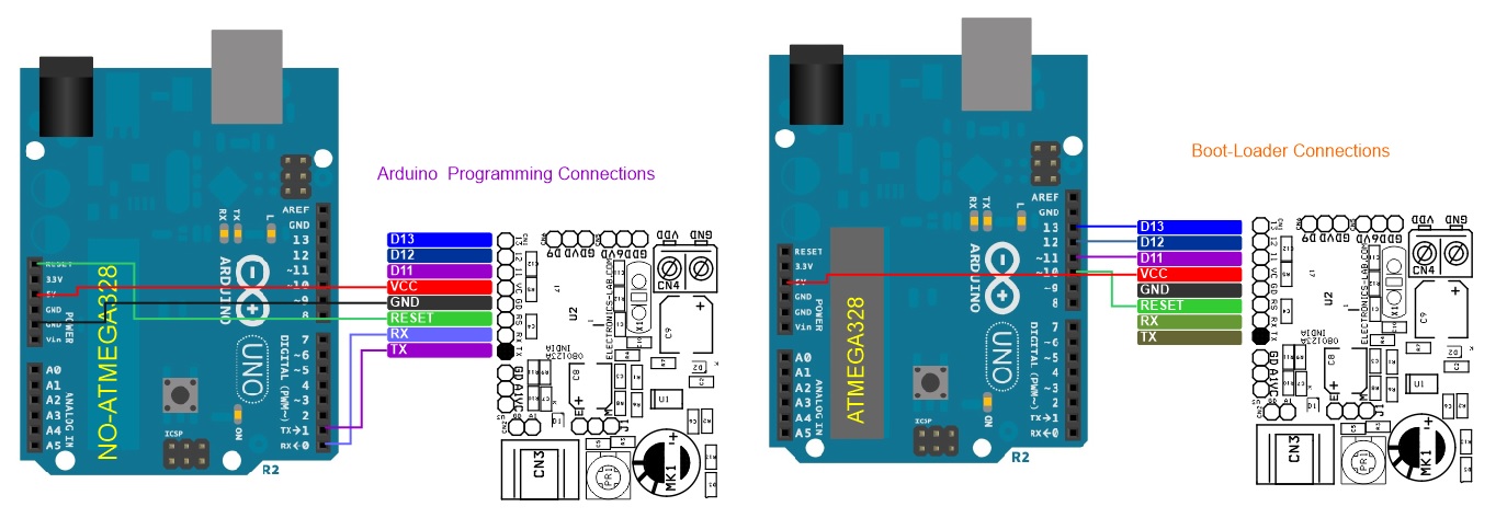
The project is Arduino compatible and an onboard connector is provided for the boot-loader and Arduino IDE programming. Arduino code is available as a download, and Atmega328 chips must be programmed with a bootloader before uploading the code. Users may modify the code as per requirement. More information on burning the bootloader is here: https://www.arduino.cc/en/Tutorial/BuiltInExamples/ArduinoToBreadboard
Direct Audio Input: The audio input signal should not exceed 5V, It is important to maintain the input audio signal at this maximum level, otherwise it can damage the ADC of ATMEGA328.
Features
Supply 5V to 6V DC (Battery Power Advisable)
RC Servo Movement 180 Degrees with Loud sound
Direct Sound Input Facility Using 3.5MM RC Jack
On Board Jumper Selection for Micro-Phone Audio or External Audio Signal
On Board Trimmer Potentiometer to Adjust the Signal Sensitivity
Flexible Operation, Parameters Can be Changed using Arduino Code
/*
 Controlling a servo position using a potentiometer (variable resistor)
 by Michal Rinott <http://people.interaction-ivrea.it/m.rinott>

 modified on 8 Nov 2013
 by Scott Fitzgerald
 http://www.arduino.cc/en/Tutorial/Knob
*/

#include <Servo.h>

Servo myservo;  // create servo object to control a servo

int potpin = A2;  // analog pin used to connect the potentiometer
int val;    // variable to read the value from the analog pin

void setup() {
  myservo.attach(9);  // attaches the servo on pin 9 to the servo object
}

void loop() {
  val = analogRead(potpin);            // reads the value of the potentiometer (value between 0 and 60)
  val = map(val, 0, 60, 0, 180);     // scale it for use with the servo (value between 0 and 180)
  myservo.write(val);                  // sets the servo position according to the scaled value
  delay(15);                           // waits for the servo to get there
}
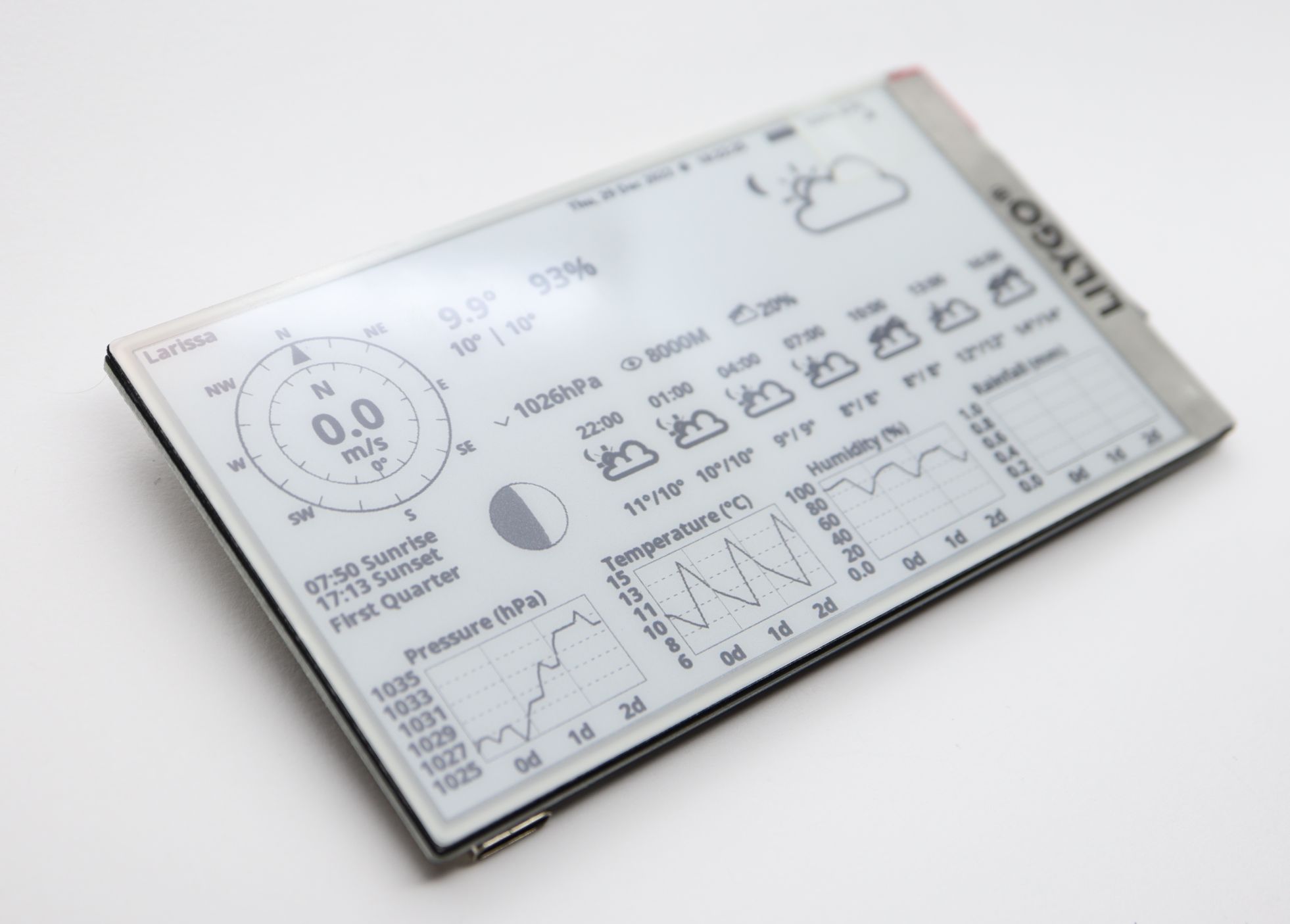
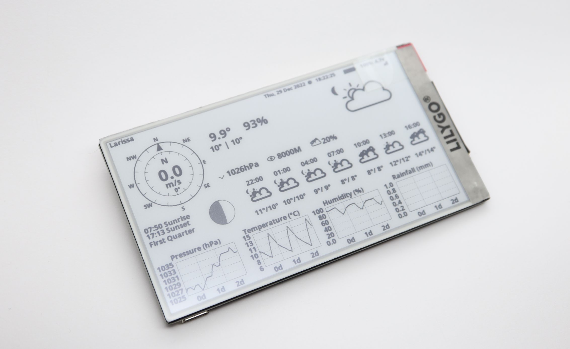
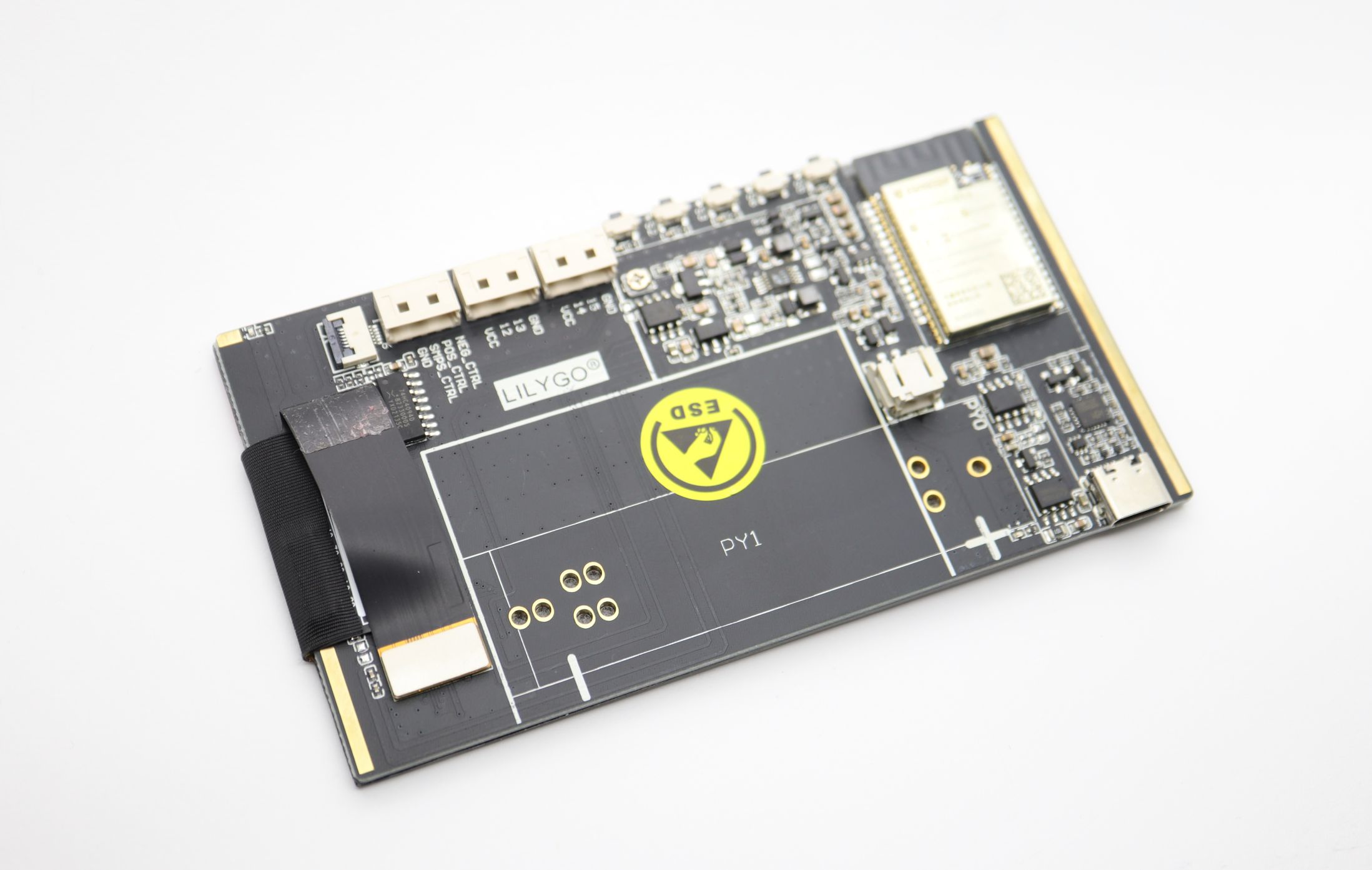
The LILYGO T5 4.7 inchE-Paper ESP32 Development Board is an exciting 4.7″ e-paper display integrated with an ESP32 WiFi/Bluetooth module. The board’s processor is ESP32-WROVER-E with 16MB of FLASH memory and 8MB of PSRAM. The ESP32 module supports Wi-Fi 802.11 b/g/n and Bluetooth V4.2+BLE and can easily be programmed with Arduino IDE, VS Code, or ESP-IDF. The board can be purchased on Aliexpress for 56.65 EUR + shipping or Tindie for 39.40 USD + shipping. This display is ideal for building a weather station that fetches weather data from OpenWeatherMap via simple API usage. So in this tutorial, we will follow the steps to make a weather station like the photo above. We will work on a Windows PC to program the display, but the same can be done in Linux or Mac OS.
Specifications
MCU: ESP32-WROVER-E (ESP32-D0WDQ6 V3)
FLASH: 16MB
PRAM: 8MB
USB to TTL: CP2104
Connectivity: Wi-Fi 802.11 b/g/n & Bluetooth V4.2+BLE
Onboard functions: Buttons: IO39+IO34+IO35+IO0, Battery Power Detection
Power Supply: 18650 Battery or 3.7V lithium Battery (PH 2.0 pitch)
First of all, we will need to install the USB to Serial (CH343) Drivers if we don’t have this done previously. Depending on your Windows version you will need:
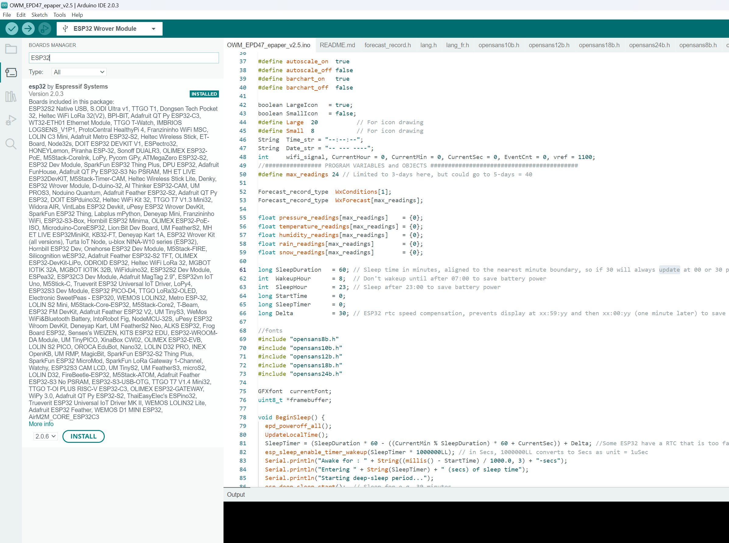
Next click Tools, and select Boards: -> Boards Manager . It will open the left pane with a list of boards. Type ESP32 into the search field. Find ESP32 by Espressif Systems, and click Install.
Preparing the Code
Download LilyGo-EPD47 library to the C:\Users\YOUR_USERNAME\Documents\Arduino\libraries folder on your system:
Download and extract LilyGo-EPD-4-7-OWM-Weather-Display to your directory with Arduino projects. This directory is normally located in C:\Users\YOUR_USERNAME\Documents\Arduino.
The project folder name should match the name of the source code file (OWM_EPD47_epaper_v2.5). This is done to avoid the unnecessary step of moving the files later.
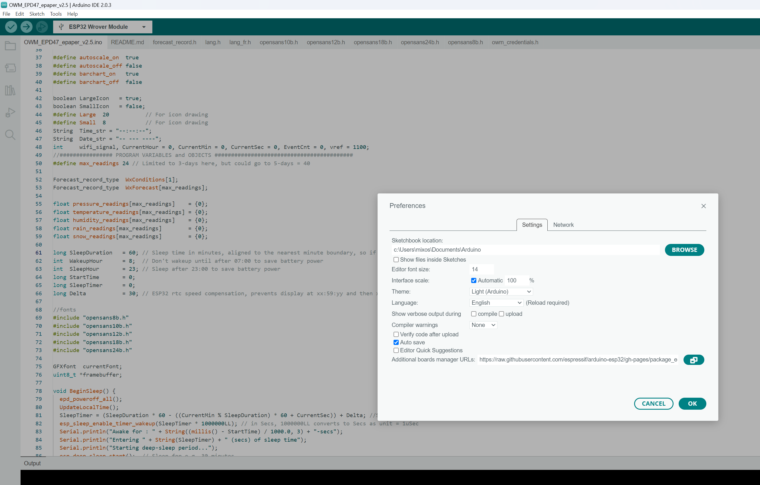
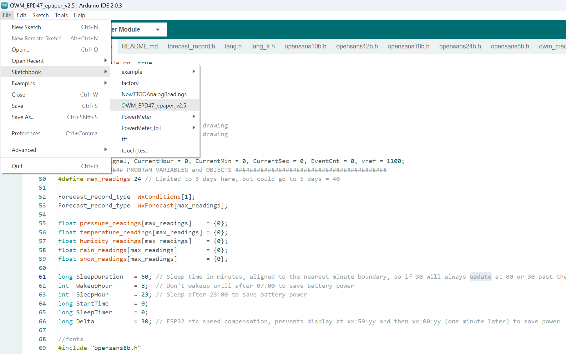
Open Arduino IDE 2.0, click File, -> Sketchbook, -> OWM_EPD47_epaper_v2.5.
The sketch requires ArduinoJson Library to successfully build.
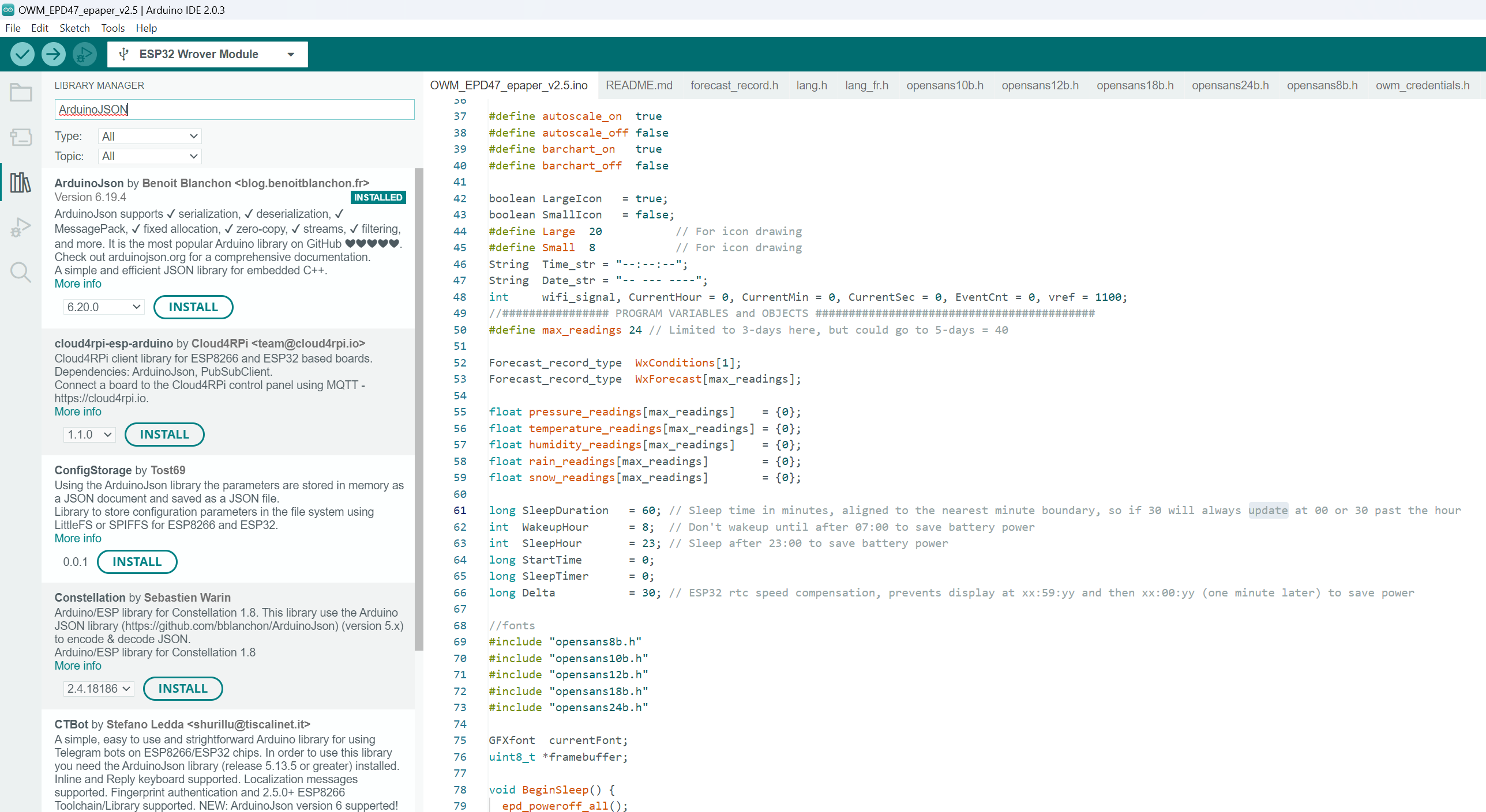
Click Tools, ->Manage libraries. The pane with Library Manager will open, then type ArduinoJson into the search field. Find ArduinoJson by Benoit Blanchon, click Install.
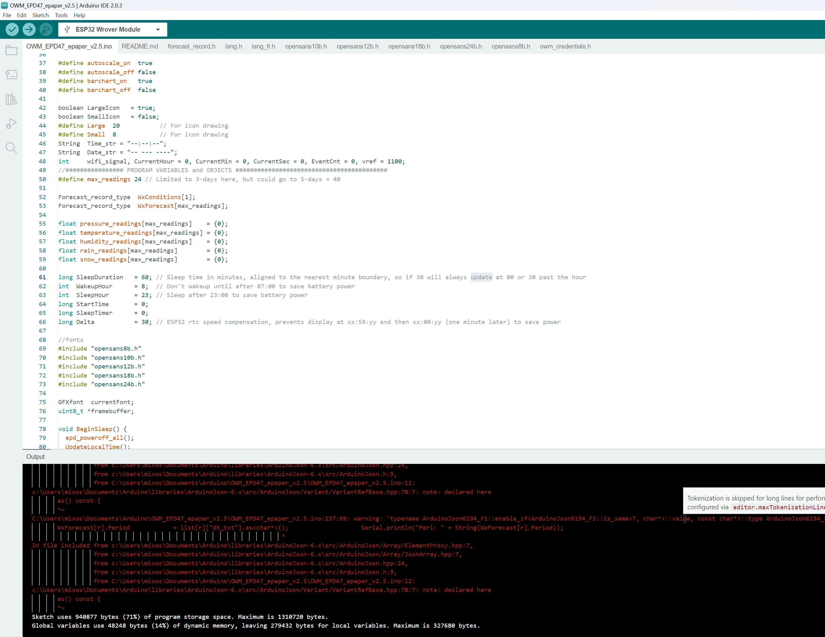
Then click the tick button on the top menu to compile the code. If everything is successful it should show:
Once you verify that the code is compiled you can move on to the next step.
Configuring Parameters
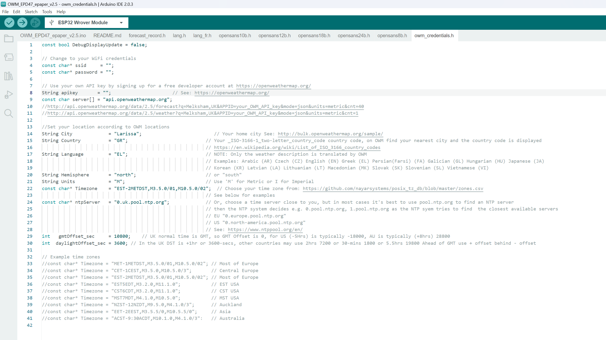
Open the file owm_credentials.h and configure ssid, password, apikey, City, and Country.
The project is fetching data from openweathermap.org so you will need to create a new free account in order to get API key.
Power Saving
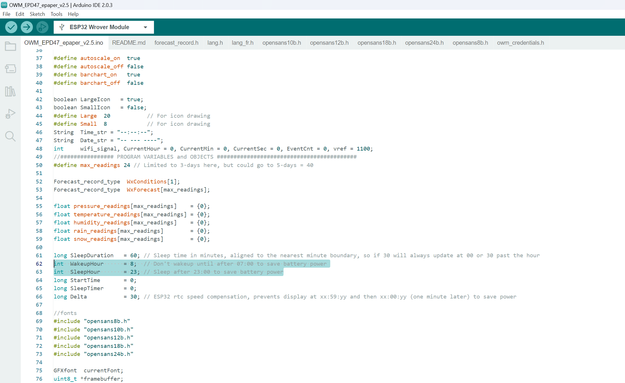
The project code supports power saving, so if you’re flashing in the early before 08.00 or after 23.00, you might notice that nothing appears on the display.
To change the power-saving options open file OWM_EPD47_epaper_v2.5.ino and change WakeupHour and SleepHour to a value that suits your schedule.
Uploading the Code
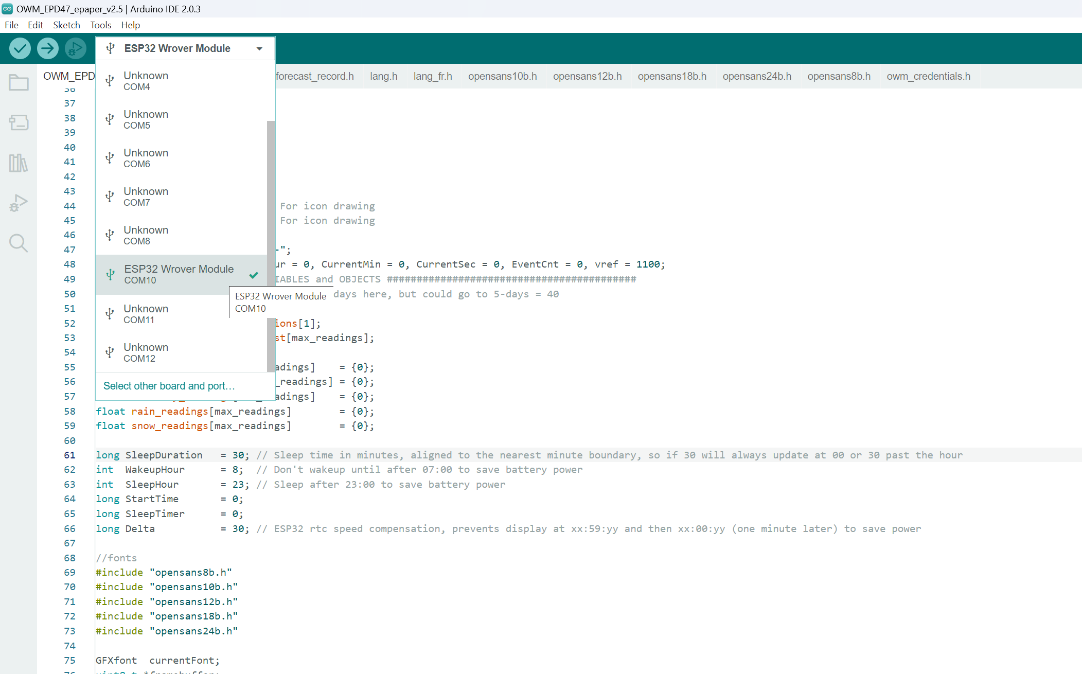
Connect the LilyGO T5 4.7-inch e-paper display to your PC-> Select the board from the dropdown in the toolbar. Search for the ESP32 Wrover module and click Ok.
Click the Upload button.
If the flashing is successful, your weather will be displayed on the e-paper like the photos below.
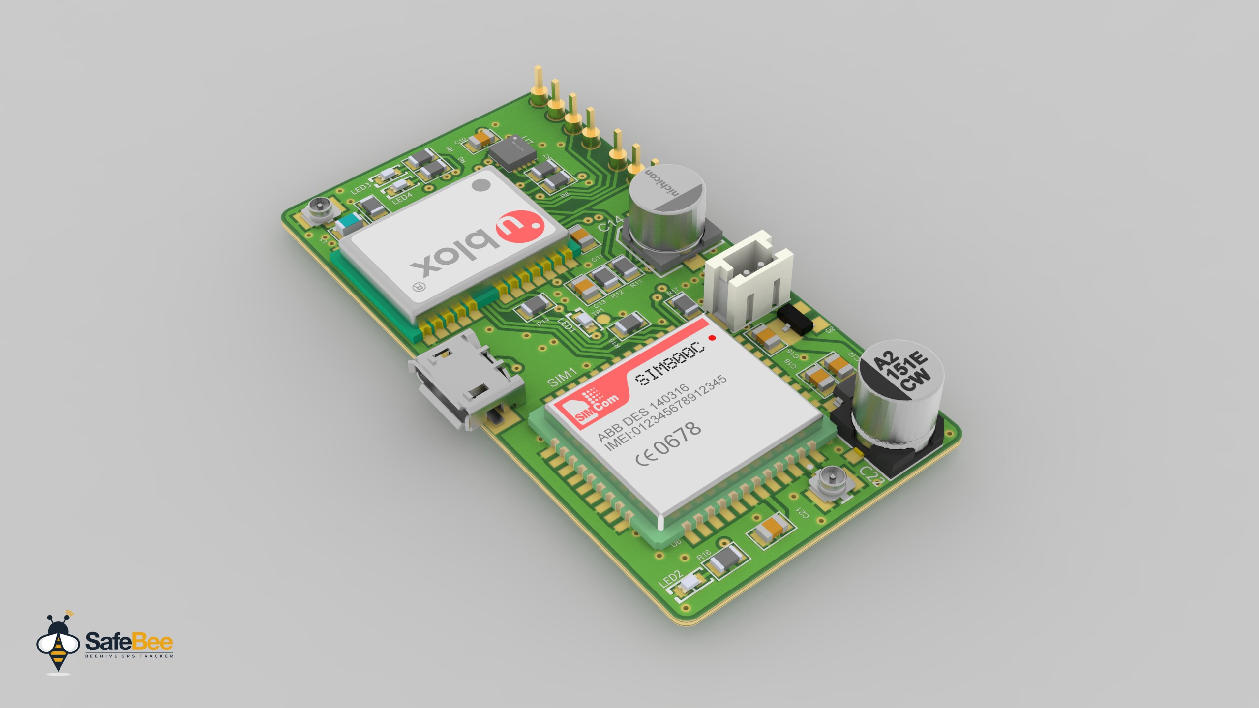
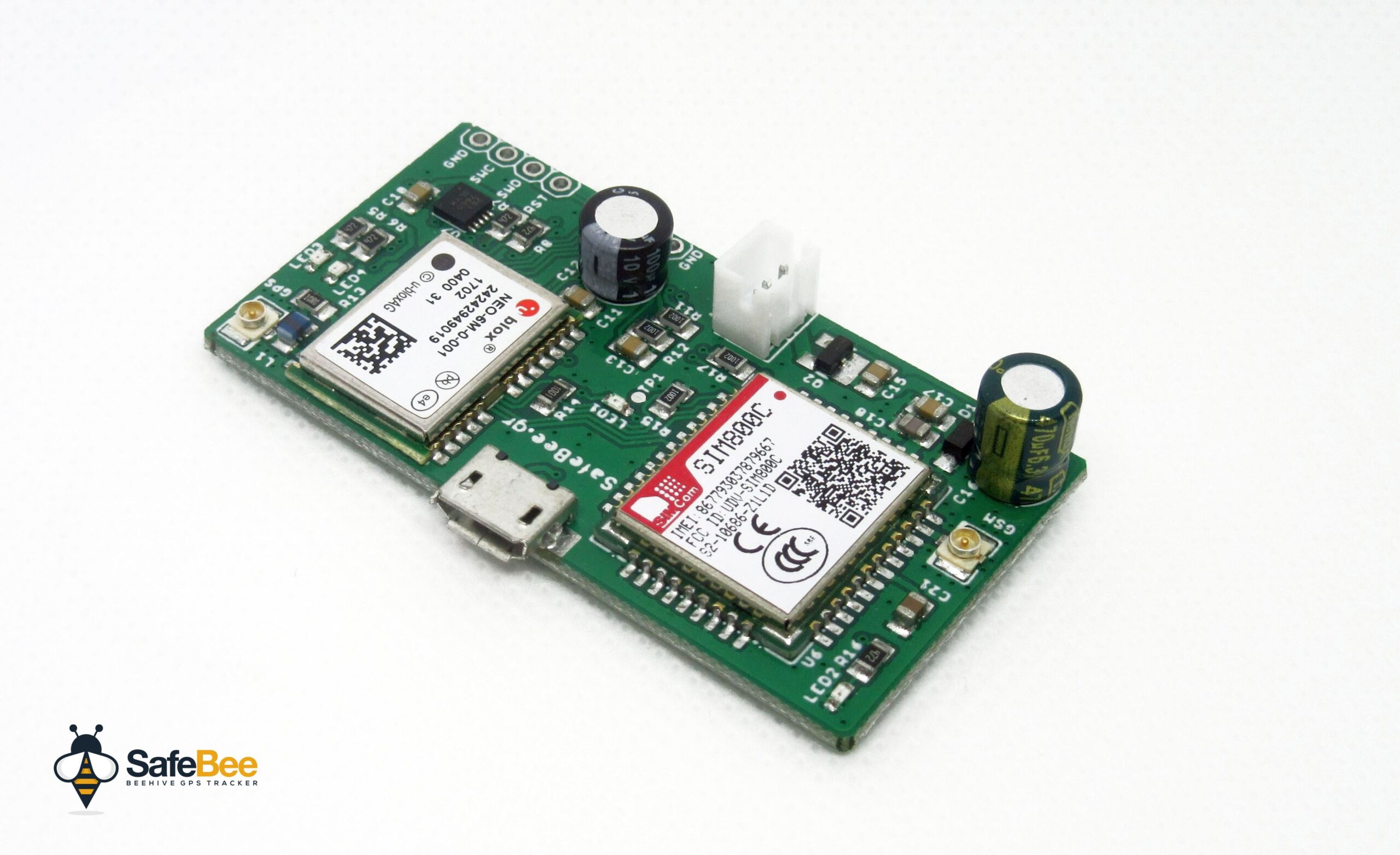
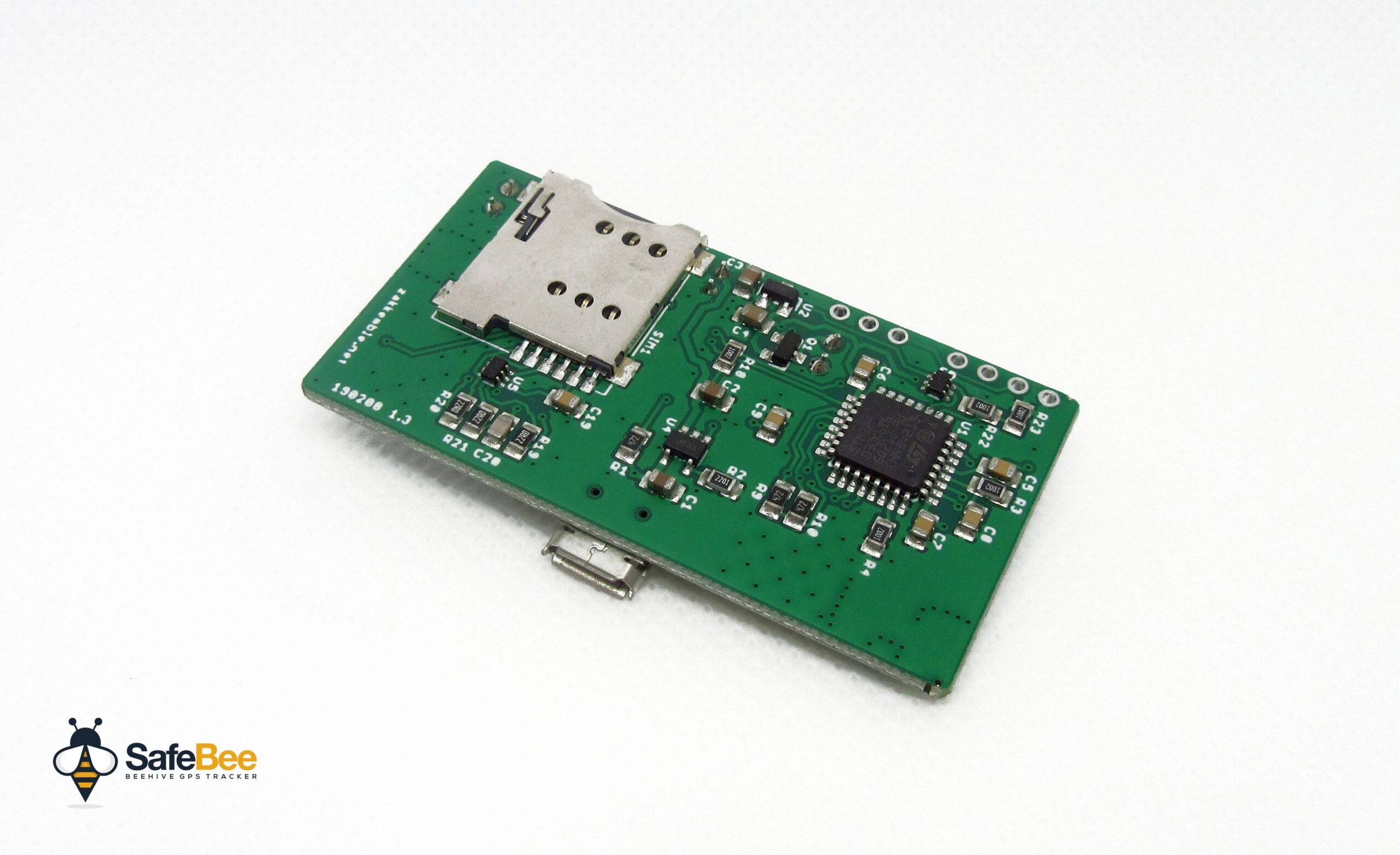
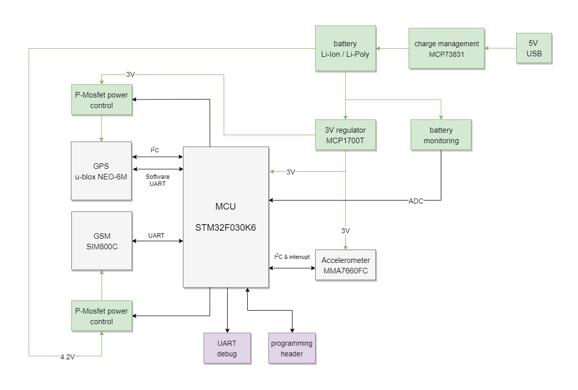
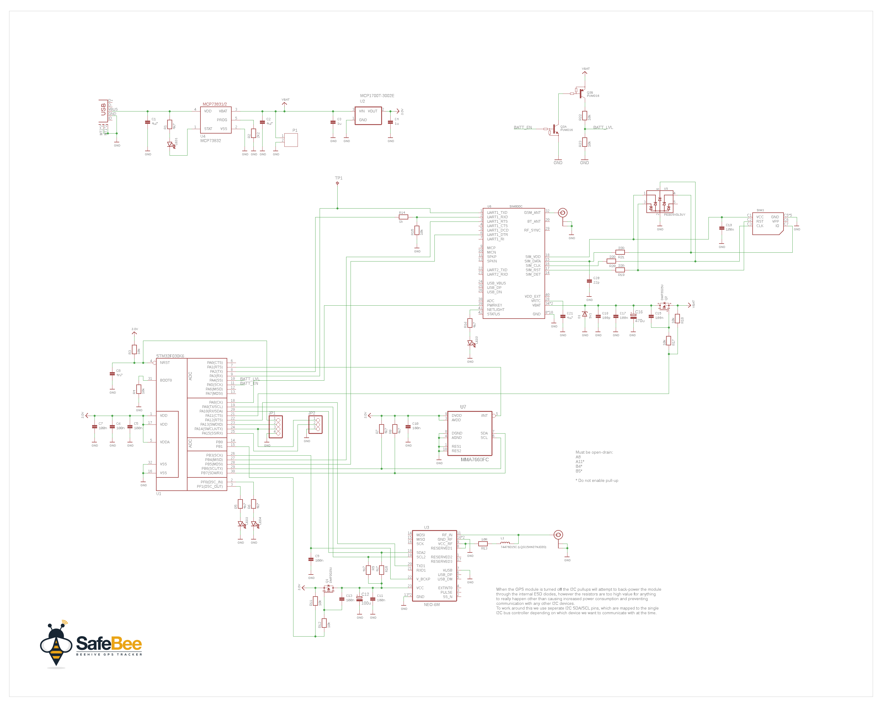
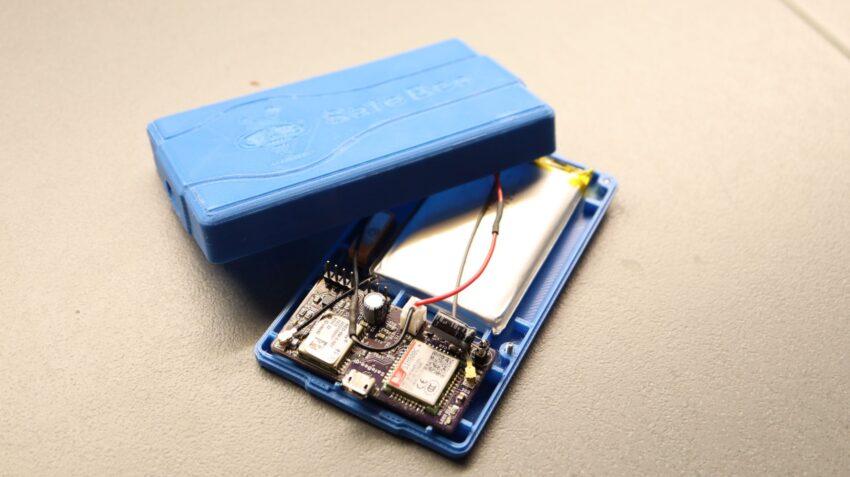
This is an original design of a GPS tracker designed on Elab and it is intended to be used as a security device for beehives, but it is not limited to this. It can be used everywhere a motion-activated GPS tracker is needed, like your car, bike, or even your boat. It is a GPS tracker controlled by simple SMS commands and designed for reliability,low power consumption, and easeof use. It features a MEMS accelerometer that is used to intelligently detect movement and once triggered it will power on the GPS module and will try to acquire the current coordinates. The location details will be transmitted to the owner’s smartphone via a simple SMS and then follow update the coordinates at predefined intervals.
Key Features:
Remote management via simple SMS commands
High reliability – no need to babysit the tracker due to crashes and resets
Long battery life – over 1 year standby on a single charge (2500mAh battery)
3-axis high-sensitivity MEMS Accelerometer
Intelligent Triggering – it will not be triggered by accidental movement
Selectable Trigger Sensitivity Level
Description of Operation
The tracker has 3 main modes of operation, detailed below:
Standby
Ready
Tracking
Standby mode
In standby mode, the GSM and GPS modules are powered down and the microcontroller is in sleep mode, resulting in a current draw of approximately 70uA, mainly by the accelerometer (MMA7660). The accelerometer is used to detect movement caused by a possible thief. If the accelerometer is triggered 1 or 2 or 3 times (depending on the sensitivity level) inside of a 60-second window then the device will enter tracking mode. While in standby mode the tracker will also enter ready mode approximately every 12 hours, triggered by the microcontroller’s internal RTC. This is to check for incoming commands and battery status etc.
Ready mode
The ready mode is entered by the microcontroller’s internal RTC and when the tracker is first powered on. In this mode, the tracker will power up the GSM module and wait for any SMSs to come in and process them. The tracker will stay in ready mode for 5 minutes before returning to standby mode unless an SMS command has instructed the device to enter tracking mode (BEE+TRIGGER).
Tracking mode
Tracking mode is entered when manually instructed to by the BEE+TRIGGER command or after the accelerometer triggers (1 or 2 or 3 movements detect depending on sensitivity level) within a 60-second window, from either standby or ready modes. In tracking mode, the tracker will power up both the GSM and GPS modules and begin to send tracking alert SMSs to the number configured by the BEE+NUMBER command. The device will continue to stay in tracking mode until the BEE+CLEAR command is received or while the accelerometer is detecting movement and/or the GPS module has a lock and the speed is greater than 10KPH. If neither of these conditions is met for 6 minutes then the tracker will send a tracking stopped SMS and return to standby mode, or ready mode if the RTC was triggered within the last 5 minutes.
Power up and Battery Status
In ready and tracking modes if the battery voltage falls below the threshold voltage (3650mV default) then a low battery alert SMS will be sent to the number configured by BEE+NUMBER. Approximately every 30 days (60 RTC triggers) an automated status SMS is also sent to the number configured by BEE+NUMBER.
When power is first applied to the device the tracker will be in ready mode and it will check for incoming SMS and then go to sleep. This is the ideal time to configure the tracker with the BEE+NUMBER number. This is the number that tracking messages, monthly status reports, and low battery alerts will be sent. The phone number is stored in the microcontroller’s FLASH memory and it will be permanently saved, even if battery power is removed. At power-up, the tracker will send a status SMS and also ignore any movement detected by the accelerometer for the first 60 seconds.
The Hardware
Hover images for details
Block Diagram
MCU
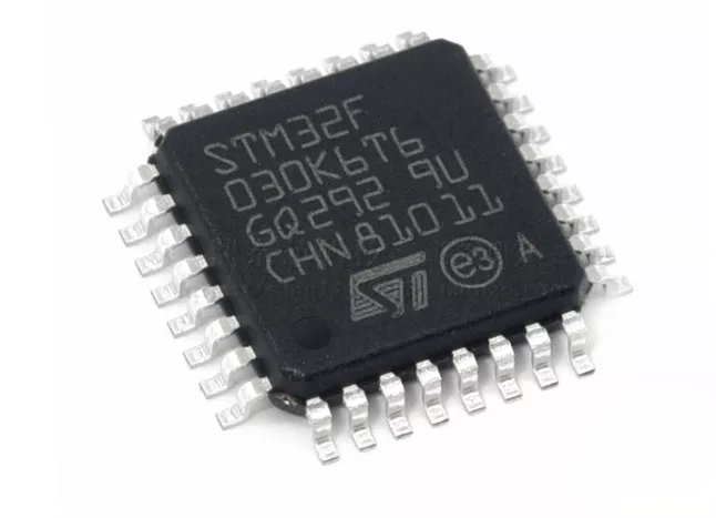
STM32F030K6
The tracker uses an ST STM32F030K6 microcontroller (ARM Cortex-M0, 32-bit RISC core), with 32KB of flash, and 4KB of RAM, and operates at up to 48MHz. The STM32F030K6 microcontroller operates in the -40 to +85 °C temperature range from a 2.4 to 3.6V power supply. A comprehensive set of power-saving modes allows the design of low-power applications. Currently, the firmware is taking roughly 24KB of flash (with debugging output enabled) and 1.7KB of RAM. The microcontroller is running at 8MHz and is supplied with 3V.
GSM module
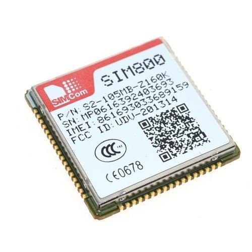
SIMCom SIM800C
The GSM module is a SIMCom SIM800C and uses the UART bus to communicate with the MCU. The GSM module is power-gated with a P-MOSFET, controlled by the MCU, as its own low-power modes are not sufficient for this project. SIM800C supports Quad-band 850/900/1800/1900MHz, it can transmit Voice, SMS and data information with low power consumption. With a tiny size of 17.6*15.7*2.3mm, it can smoothly fit into our small board. The module is controlled via AT commands and has a supply voltage range 3.4 ~ 4.4V.
GPS module
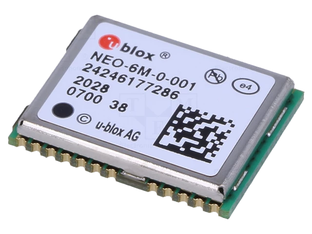
u-blox NEO-6M
The GPS module is a u-blox NEO-6M and uses the I2C bus to communicate with the MCU. There is also a UART connection to the microcontroller as a fallback if the I2C interface does not work (usually the case with Chinese fakes). So, the tracker will work with the original NEO-6M as well as Chinese fake modules. The microcontroller implements the UART interface in software (via timer interrupts), operating at 9600 baud. The GPS module is power-gated with a P-MOSFET, controlled by the MCU, as its own low-power modes are not sufficient. The NEO-6M is powered in the range of 2.7 – 3.6V and has a size of 12.2 x 16 x 2.4mm. More details and design considerations can be found in the Hardware Integration Manual of NEO-6 GPS Modules Series and u-blox 6Receiver Description.
Supported GPS modules:
U-blox NEO-5M
U-blox NEO-6M
U-blox NEO-7M
U-blox NEO-M8N
Various Chinese fakes using AT6558 and similar (if the PCB footprint is the same then it will probably work)
Accelerometer
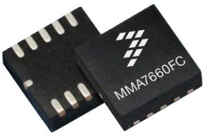
MMA7660FC
The accelerometer IC is the MMA7660FC and uses the I2C bus to communicate with the MCU. The MMA7660FC is a ±1.5g 3-Axis Accelerometer with Digital Output (I2C). It is a very low power, low profile capacitive MEMS sensor featuring a low pass filter, compensation for 0g offset and gain errors, and conversion to 6-bit digital values at a user-configurable sample per second. In OFF Mode it consumes 0.4 μA, in Standby Mode: 2 μA, in Active mode 47 μA and is powered in the range 2.4 V – 3.6 V. The accelerometer is always active, set up to create an interrupt whenever a shake or orientation change is detected, and is configured with a sampling rate of 8Hz (higher sampling rates improve detection, but also increase power consumption). The interrupt will wake up the microcontroller, where it will run through the main loop. In this loop it checks the interrupt status, and if set it will clear the interrupt and increment a counter at a maximum of once per second. The counter is reset every minute. If the counter reaches 3 the tracker is activated.
Battery Charger
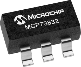
MCP73832
The Li-Ion battery charging IC is MCP73832, which has a user-programmable charge current and the battery charge rate is set to 450mA. It includes an integrated pass transistor, integrated current sensing, and reverse discharge protection. It is usually recommended to charge Lithium batteries at no more than 0.5C, so the recommended minimum battery capacity to use with the tracker is 900mAh.
With a 2500mAh battery, standby current of 70uA, and waking up every 12 hours for 5 minutes with an estimated average current of 15mA the battery life should be approximately 1.5 years. A poor GSM signal can reduce battery life.
Status LEDs
LED
Description
States
LED1
Battery charging state
OFF: Battery not charging (no USB power or battery fully charged) ON: Charging
LED2
GSM state
OFF: GSM is powered off FAST BLINK: GSM is not connected to a network (usually no signal or no SIM) SLOW BLINK: GSM is connected to the network
LED3
MCU Operating mode
OFF: Standby mode ON: Ready or tracking mode
LED4
GPS state
OFF: GPS is powered off FAST BLINK: GPS is acquiring a lock SLOW BLINK: GPS has a lock
SMS Commands
Command
Description
BEE+STATUS
Returns battery voltage - temperature - GSM signal strength - tracking enabled - is tracking - last GPS coordinates -sensitivity level.
BEE+CLEAR
If the tracker has been triggered this will clear it and stop tracking until the next trigger.
BEE+TRIGGER
Manually trigger tracking (will trigger even if disabled with BEE+DISABLE). Tracking will stay enabled until BEE+CLEAR is received.
BEE+ENABLE
Enable tracking triggers
BEE+DISABLE
Disable tracking triggers.
BEE+NUMBER=0123499988
This sets the mobile number to send tracking - low battery warning and monthly status SMSs to. Other command replies are sent to the number that the command was sent from.
BEE+NUMBER=+441234999888
International numbers must start with + then the country code.
BEE+SENSE=1/2/3
This is the sensitivity level - 1 high sensitivity - 2 medium sensitivity - 3 low sensitivity.
LOW BATTERY: (battery voltage)mV (threshold voltage mV)
LOW BATTERY: 3400mV (3650mV)
Programming
The device firmware can be programmed via the SWD interface, which is the 4-pin programming header on the PCB marked RST (reset), SWD (SWDIO), SWC (SWCLK) and GND (ground). An ST-LINK/V2 USB adapter is needed to program the device, which is available from ebay, aliexpress, and other places for less than £3.
3D Render
3D Render of the board on KeyShot 11 Pro
Debugging
Debugging data is sent out of the UART interface through the TX pin of the debugging header on the PCB, at 115200 baud. This pin is also shared with the SWD interface (SWC). The RX pin is unused but made available for possible use in the future.
Format
(<time>)(<module>)<message>
“time” is in milliseconds and only increments while the microcontroller is not in standby mode. “module” is either “DBG” (general messages), “TRK” (tracker), “GSM”, “GPS”, “SMS”, “MGR” (MGR is the SMS manager which controls when queued SMSs are sent, retried etc.)
A 3D model of the enclosure is designed using Solidworks with overall dimensions of 60 x 20 x 112 mm. The enclosure has two holes, one for the charging micro USB connector and one to fit a mini rocker power switch. The provided design files (download .STEP and .STL files below) can be used to print your own enclosure in your desired color and material. The screws used to secure the enclosure are M3 x 10mm countersunk screws. Design is made by professional engineer janangachandima and you can find his services on the Fiverr page.
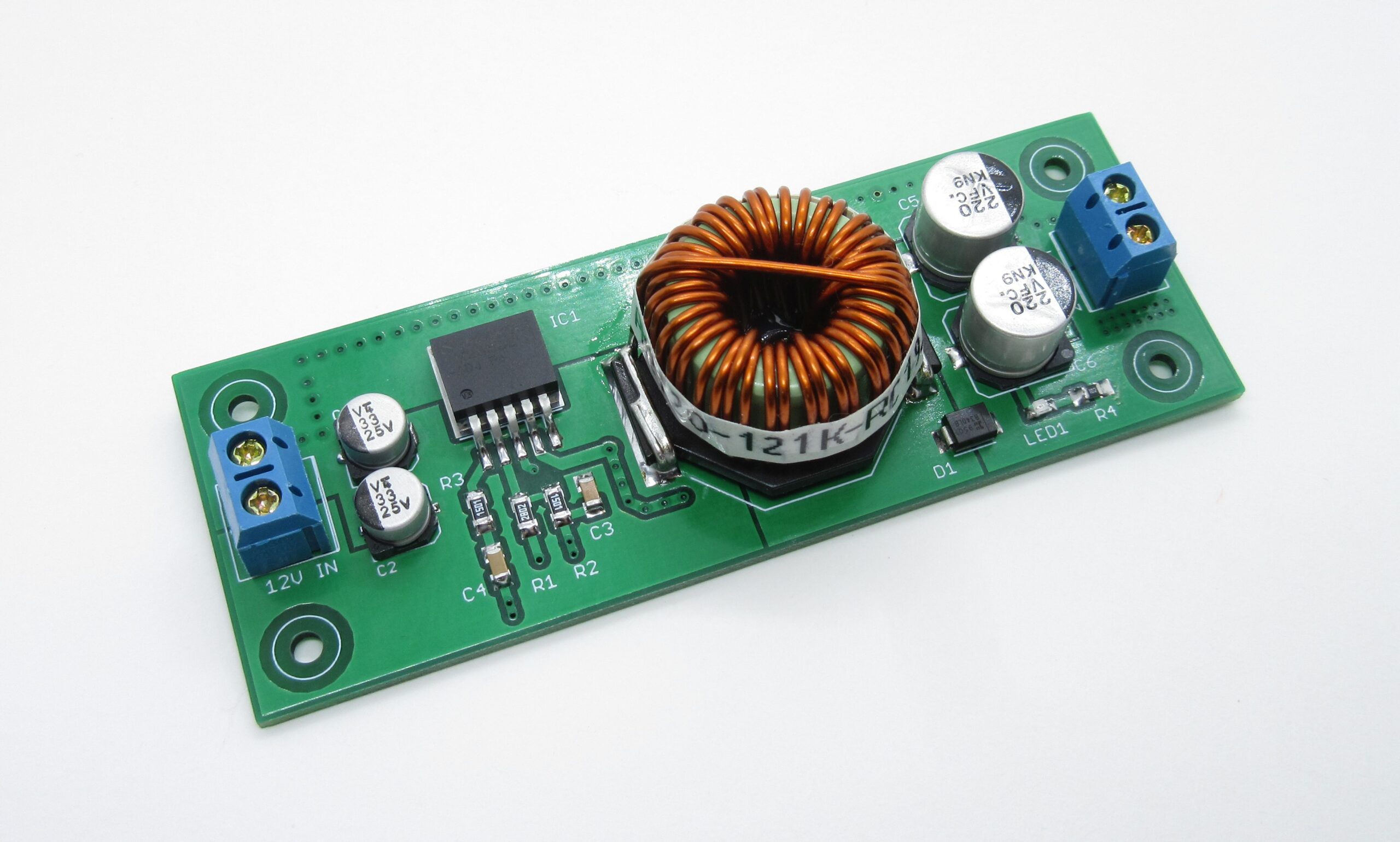
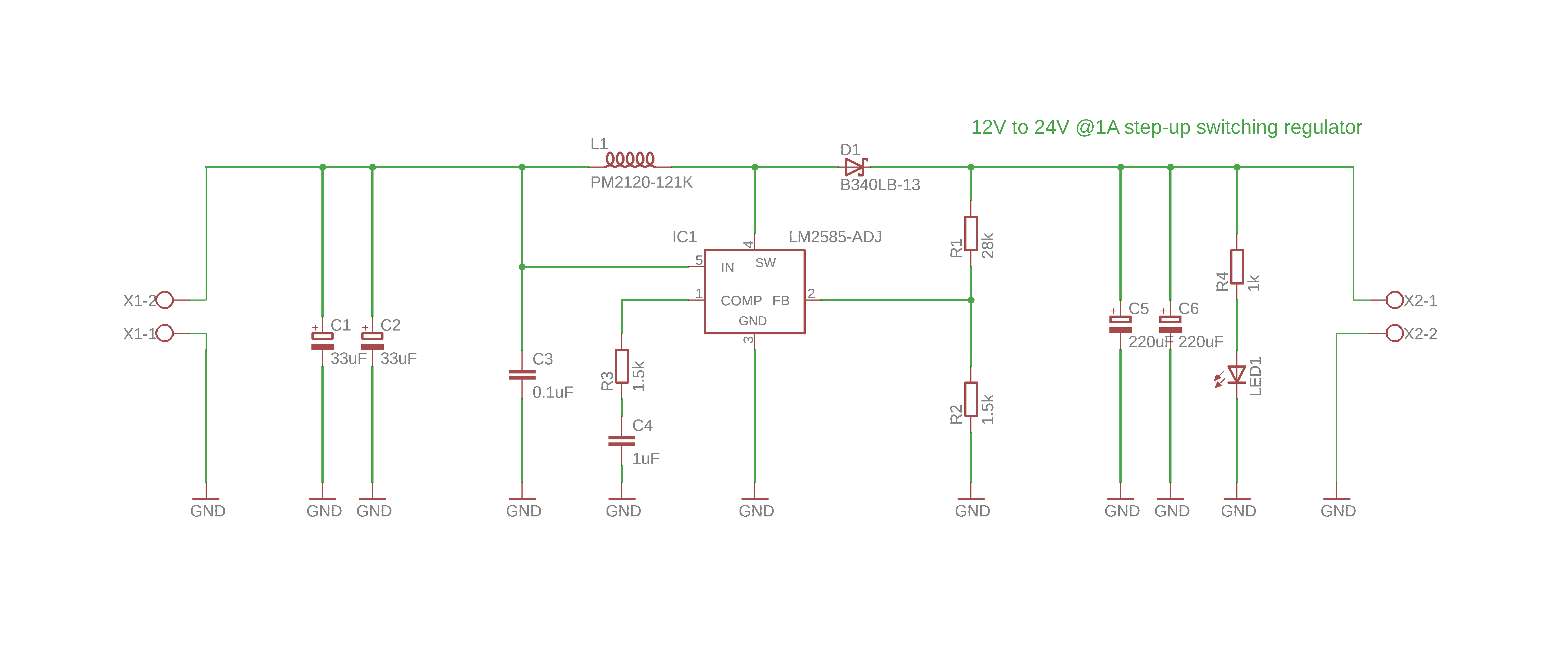
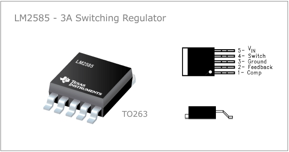
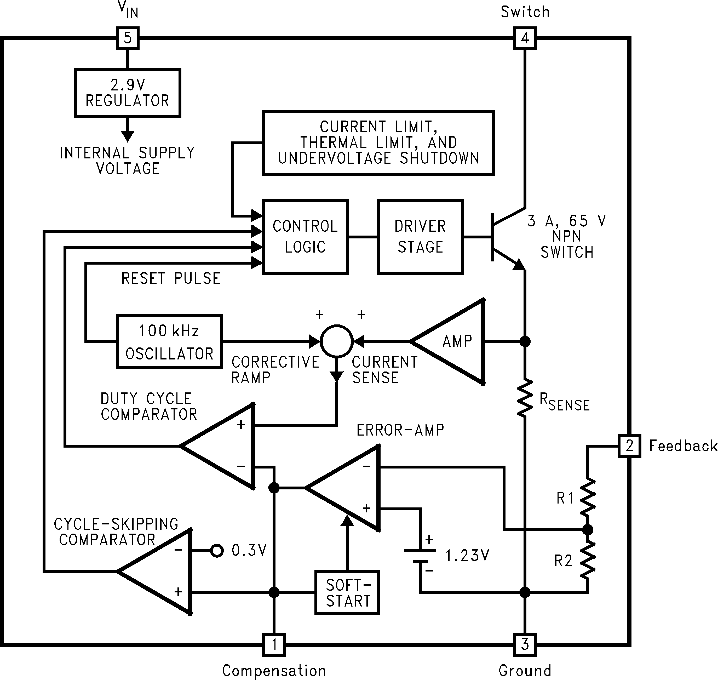
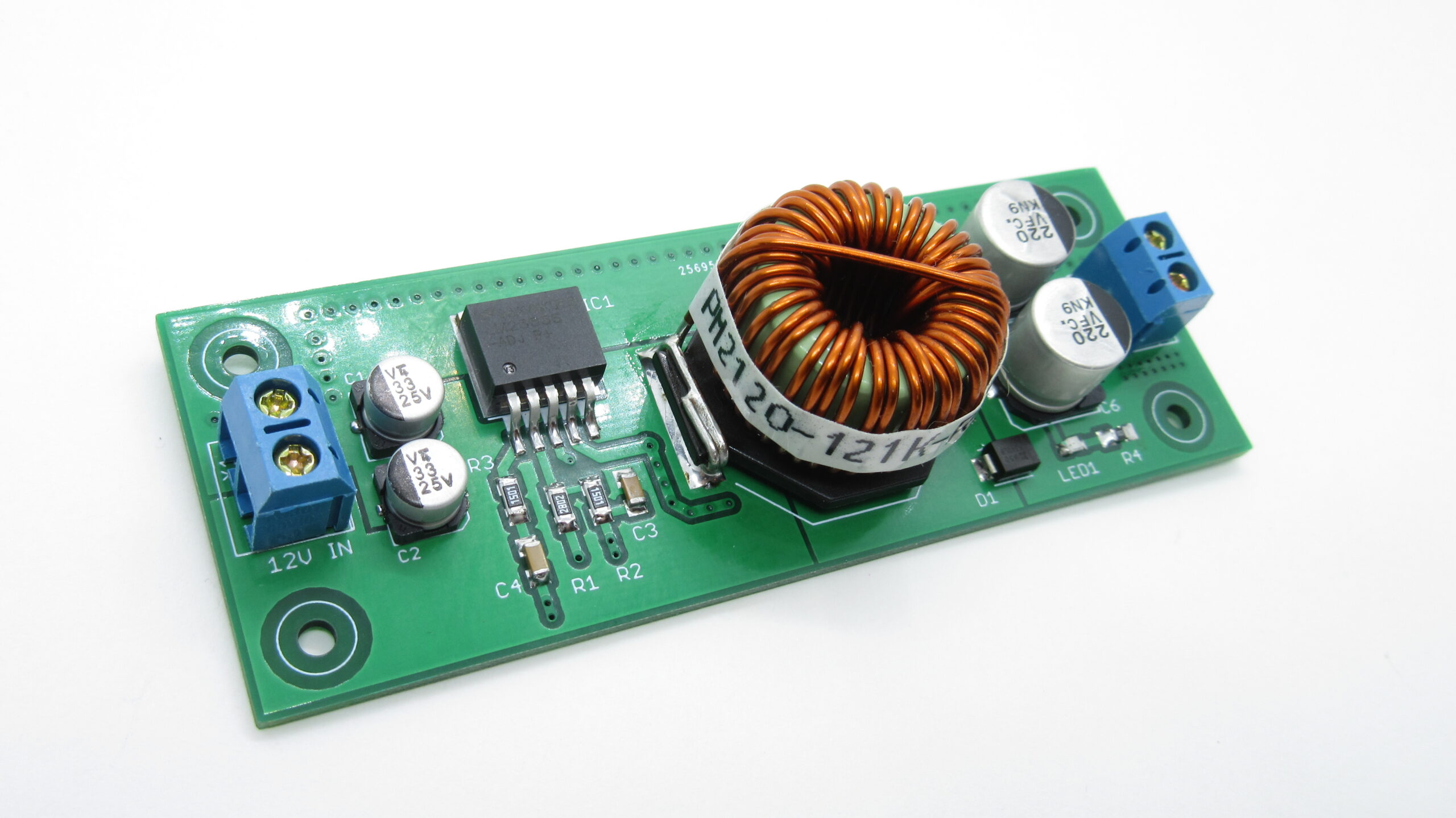
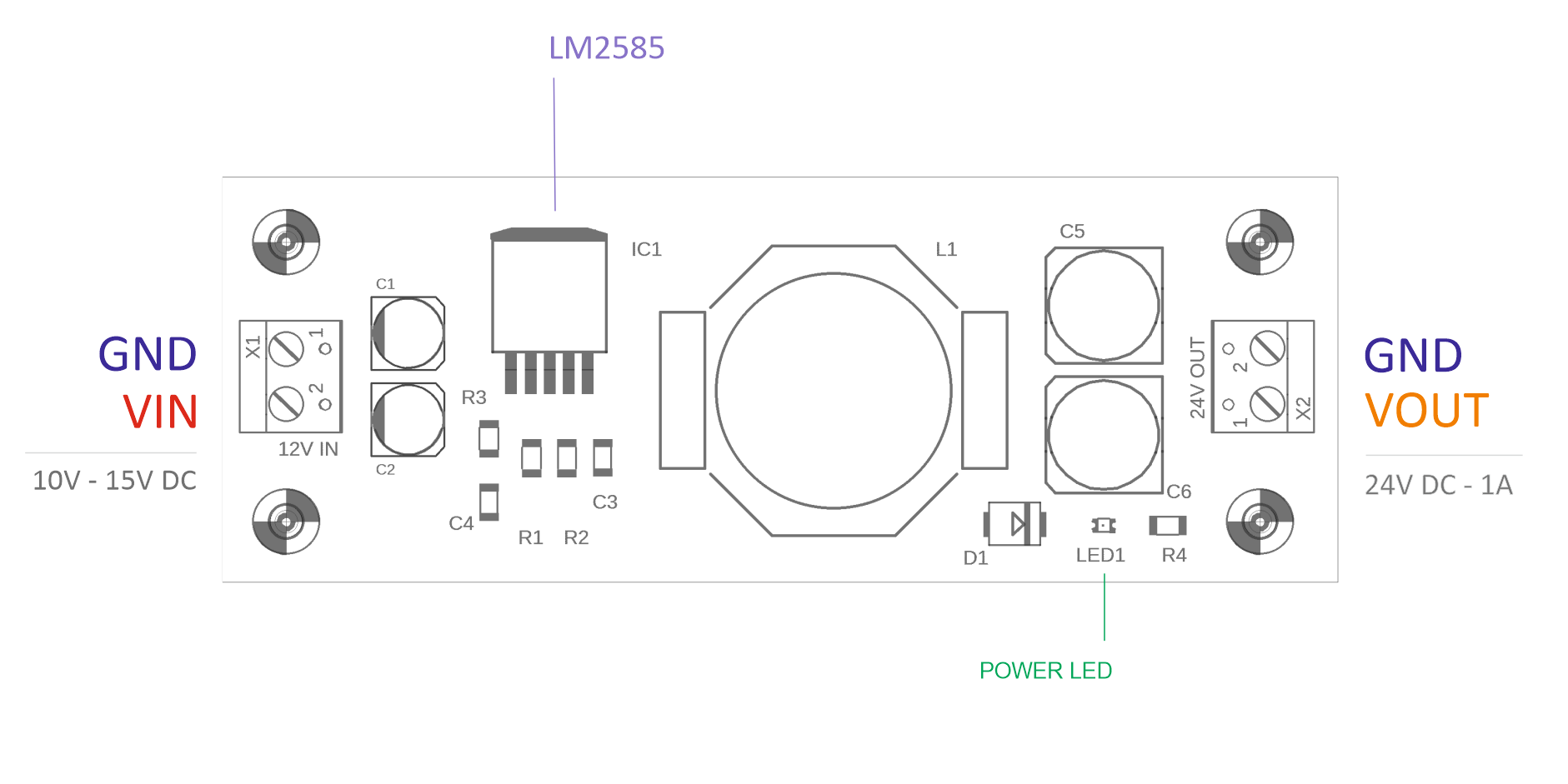
This is a DC-DC step-up converter based on LM2585-ADJ regulator manufactured by Texas Instruments. This IC was chosen for its simplicity of use, requiring minimal external components and for its ability to control the output voltage by defining the feedback resistors (R1,R2). NPN switching/power transistor is integrated inside the regulator and is able to withstand 3A maximum current and 65V maximum voltage. Switching frequency is defined by internal oscillator and it’s fixed at 100KHz.
The power switch is a 3-A NPN device that can standoff 65 V. Protecting the power switch are current and thermal limiting circuits and an under-voltage lockout circuit. This IC contains a 100-kHz fixed-frequency internal oscillator that permits the use of small magnetics. Other features include soft start mode to reduce in-rush current during start-up, current mode control for improved rejection of input voltage, and output load transients and cycle-by-cycle current limiting. An output voltage tolerance of ±4%, within specified input voltages and output load conditions, is specified for the power supply system.
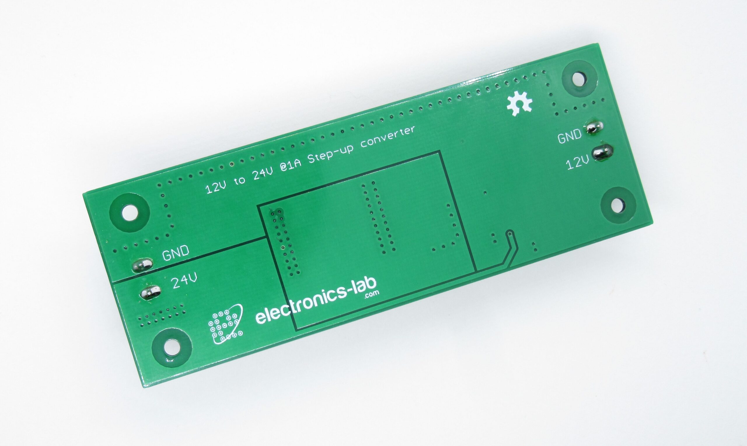
Specifications
Vin: 10-15V DC
Vout: 24V DC
Iout: 1A (can go up to 1.5A with forced cooling)
Switching Frequency: 100KHz
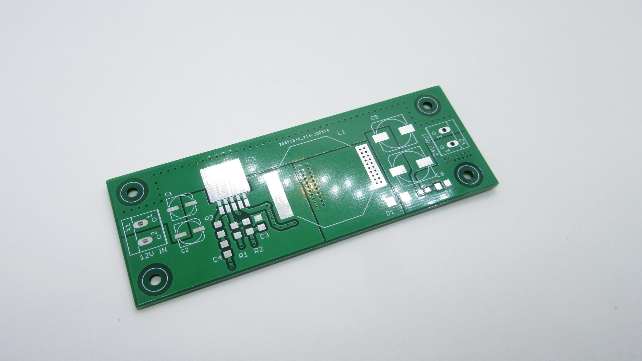
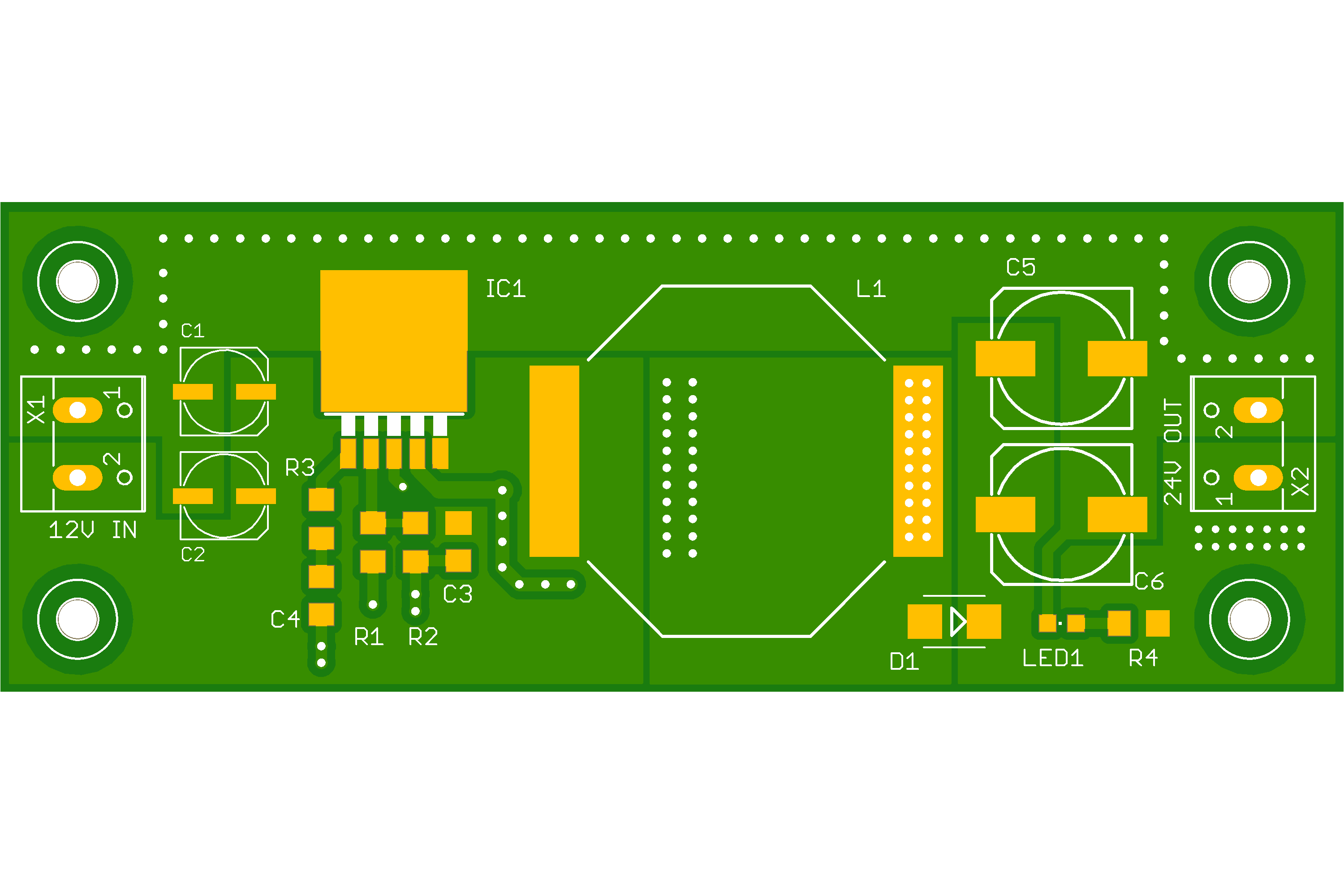
Schematic is a simple boost topology arrangement based on datasheet. Input capacitors and diode should be placed close enough to the regulator to minimize the inductance effects of PCB traces. IC1, L1, D1, C1,C2 and C5,C6 are the main parts used in voltage conversion. Capacitor C3 is a high-frequency bypass capacitor and should be placed as close to IC1 as possible.
All components are selected for their low loss characteristics. So capacitors selected have low ESR and inductor selected has low DC resistance.
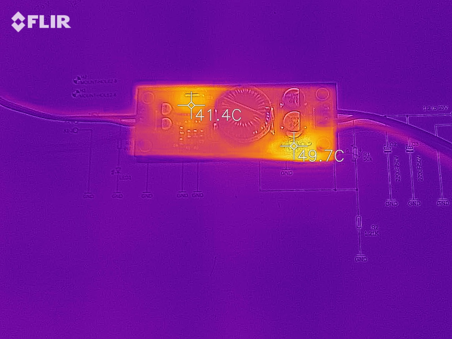
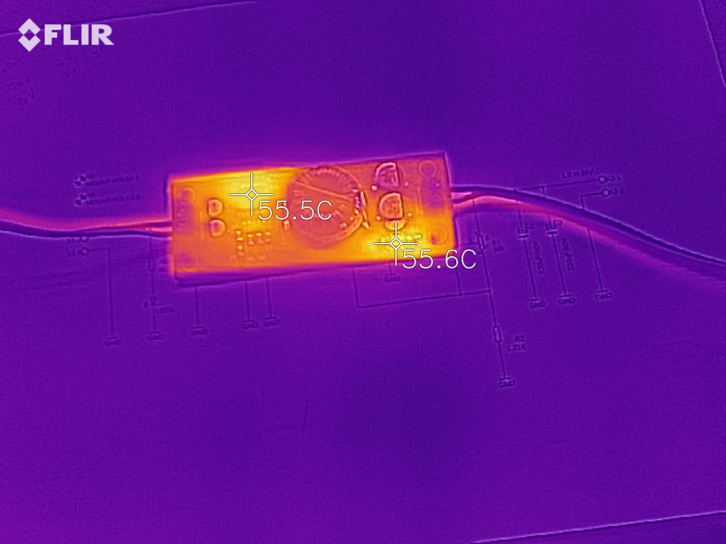
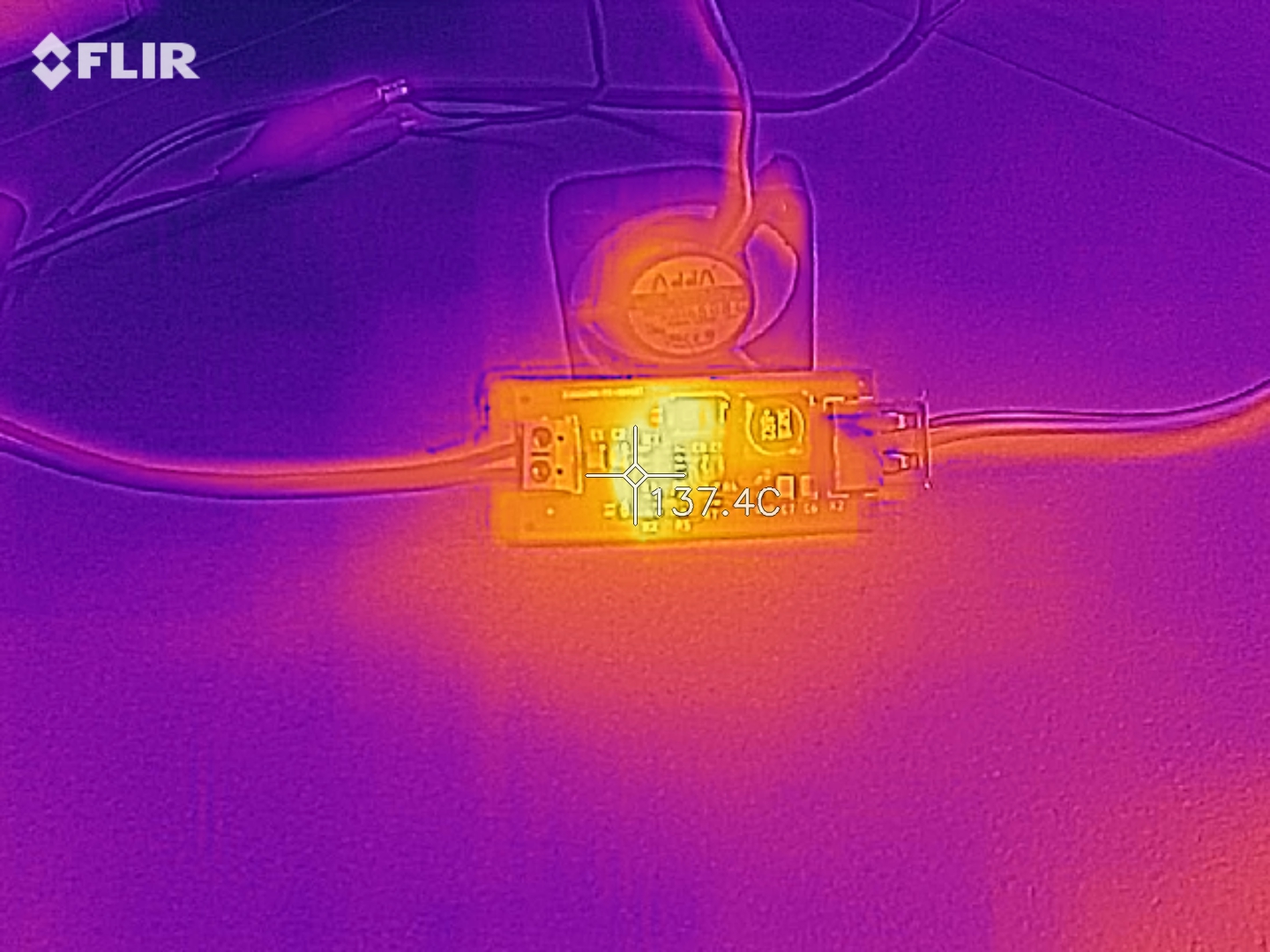
At maximum output power, there is significant heat produced by IC1 and for that reason, we mounted it directly on the ground plane to achieve maximum heat dissipation.
Block Diagram
Measurements
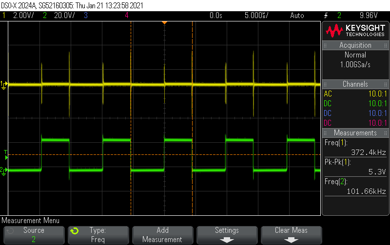
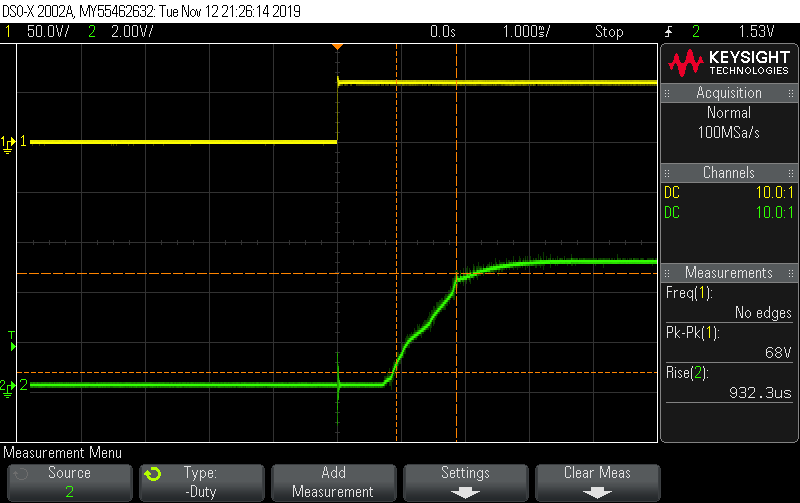
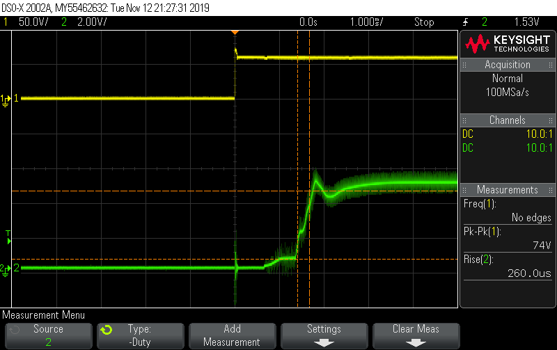
CH1: Output Voltage ripple with 12V Input and 24V @ 500mA output – 5.3 Vpp – CH2: voltage at PIN 4 of IC1CH1: Output Voltage ripple with 12V Input and 24V @ 1A output – 4.6Vpp – CH2: voltage at PIN 4 of IC1
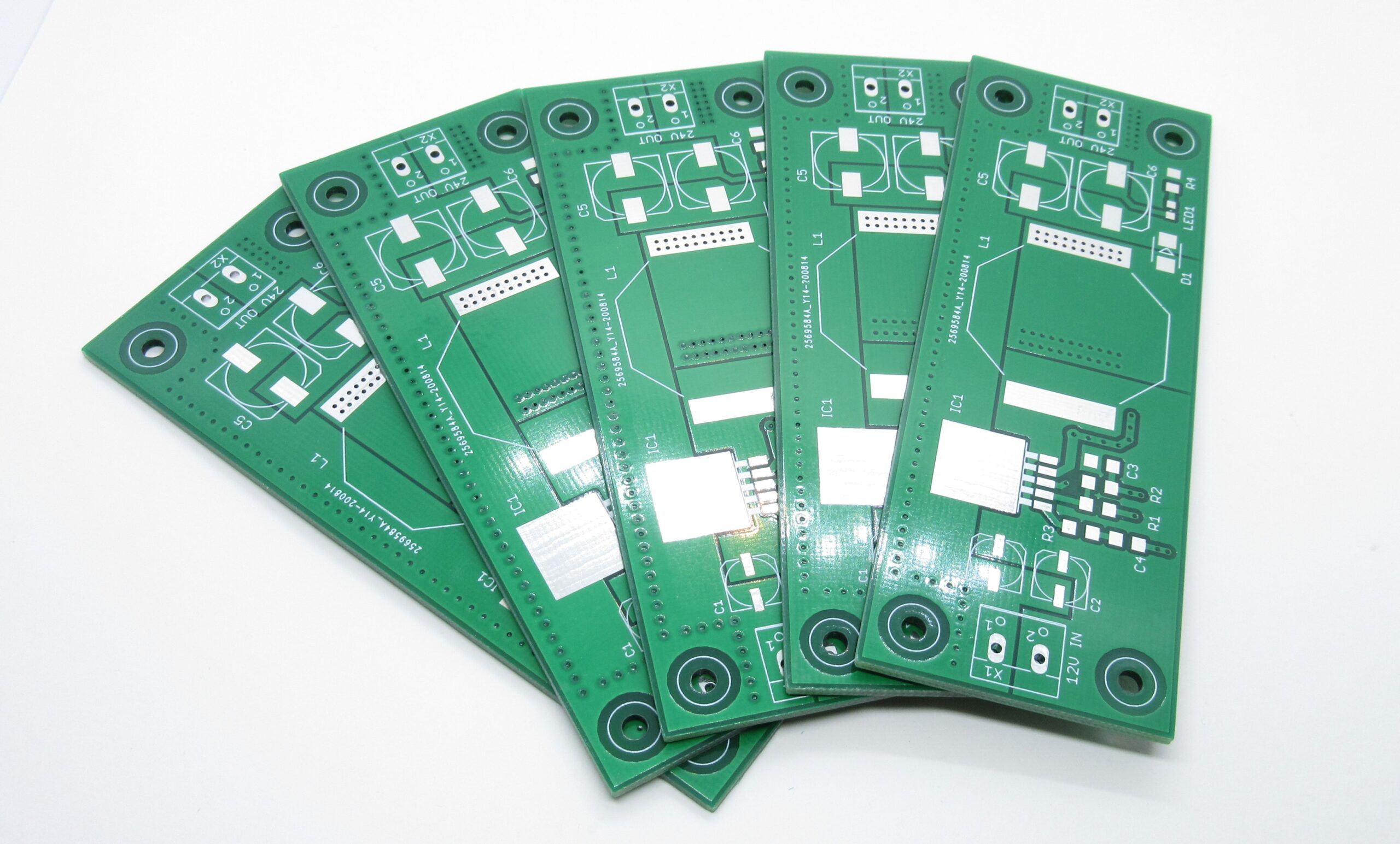
If you would like to receive a PCB, we can ship you one for 6$ (worldwide shipping) click here to contact us
Parts List
Part
Value
Package
MPN
Mouser No
C1 C2
33uF 25V 1Ω
6.3 x 5.4mm
UWX1E330MCL1GB
647-UWX1E330MCL1
C3
0.1uF 50V 0Ω
1206
C1206C104J5RACTU
80-C1206C104J5R
C4
1uF 25V
1206
C1206C105K3RACTU
80-C1206C105K3R
C5 C6
220uF 35V 0.15Ω
10 x 10.2mm
EEE-FC1V221P
667-EEE-FC1V221P
D1
0.45 V 3A 40V Schottky
SMB
B340LB-13-F
621-B340LB-F
IC1
LM2585S-ADJ
TO-263
LM2585S-ADJ/NOPB
926-LM2585S-ADJ/NOPB
L1
120 uH 0.04Ω
30.5 x 25.4 x 22.1 mm
PM2120-121K-RC
542-PM2120-121K-RC
R1
28 KΩ
1206
ERJ-8ENF2802V
667-ERJ-8ENF2802V
R2 R3
1.5 KΩ
1206
ERJ-8ENF1501V
667-ERJ-8ENF1501V
R4
1 KΩ
1206
RT1206FRE07931KL
603-RT1206FRE07931KL
LED1
RED LED 20mA 2.1V
0805
599-0120-007F
645-599-0120-007F
Connections
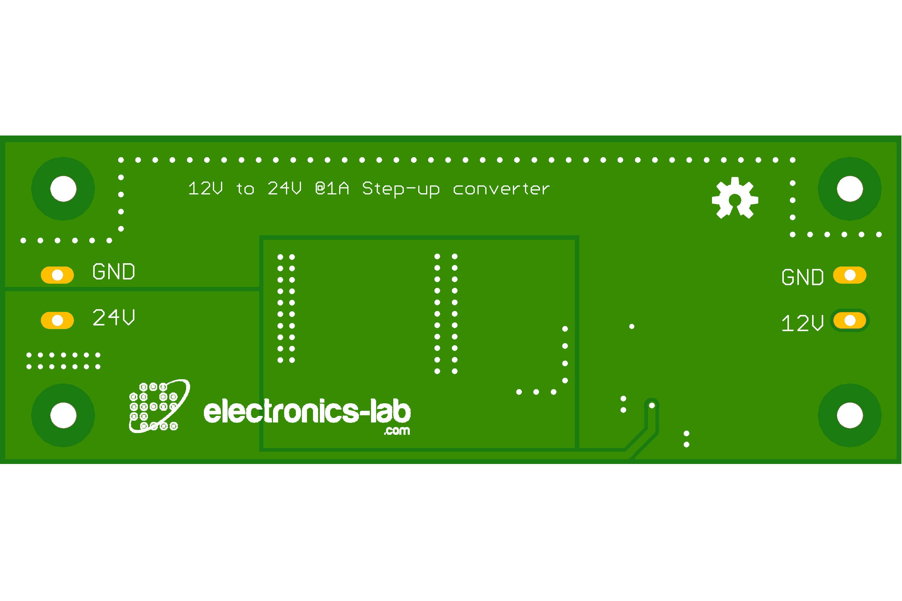
Gerber View
Simulation
We’ve done a simulation of the LM2585 step-up DC-DC converter using the TI’s WEBENCH online software tools and some of the results are presented here.
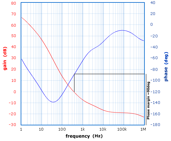
The first graph is the open-loop BODE graph. In this graph, we see a plot of GAIN vs FREQUENCY in the range 1Hz – 1M and PHASE vs FREQUENCY in the same range. This plot is useful as it gives us a detailed view of the stability of the loop and thus the stability and performance of our DC-DC converter.
Bode plot of open control loop
What’s interesting on this plot is the “phase margin” and “gain margin“. The gain margin is the gain for -180deg phase shift and phase margin is the phase difference from 180deg for 0db gain as shown in the plot above. For the system to be considered stable there should be enough phase margin (>30deg) for 0db gain or when phase is -180deg the gain should be less than 0db.
On the plot above we see that the phase margin is ~90deg and that ensures that the DC-DC converter will be stable over the measured range.
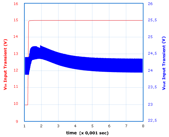
The next simulation graph is the Input Transient plot over time.
Input Transient simulation
In this plot, we see how the output voltage is recovering when the input voltage is stepped from 10V to 15V. We see that 4ms after the input voltage is stepped the output has recovered to the normal output voltage of 24V.
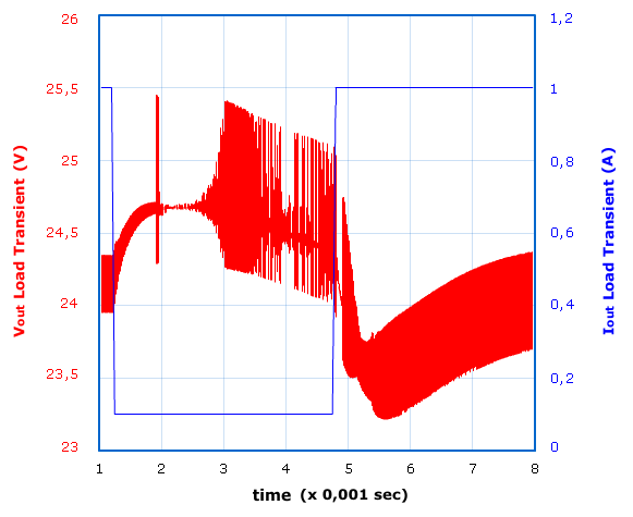
The next graph is the Load Transient.
Load Transient simulation
Load transient is the response of output voltage to sudden changes of load or Iout. We see that the output current suddenly changes from 0,1A to 1A and that the output voltage drops down to 23,2V until it recovers in about 3ms. We also see that when the load is reduced from 1A to 0,1A, output voltage spikes up to ~25,5V, then rings until it recovers to 24V in about 4ms.
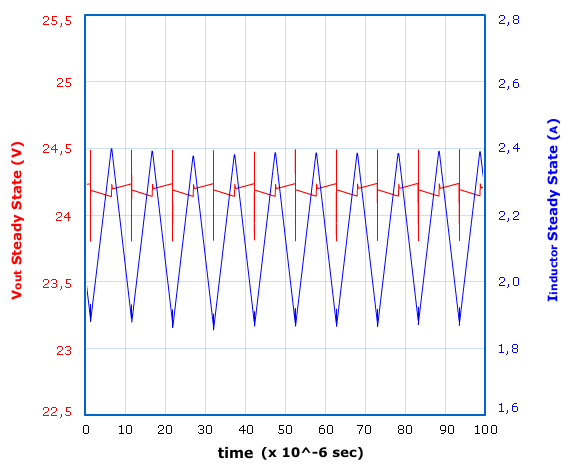
The last graph shows the Steady State operation of DC-DC converter @ 1A output.
This graph shows the simulated output voltage ripple and inductor current. We see that output voltage ripple is ~0,6Vpp and the inductor current has a peak current of 2,4A. The inductor we used is rated at max 5,6A DC so it can easily withstand such operating current and without much heating of the coil.
Operating point data (Vin=13V, Iout=1A)
Operating Values
Pulse Width Modulation (PWM) frequency
Frequency
100 kHz
Continuous or Discontinuous Conduction mode
Mode
Cont
Total Output Power
Pout
24.0 W
Vin operating point
Vin Op
13.00 V
Iout operating point
Iout Op
1.00 A
Operating Point at Vin= 13.00 V,1.00 A
Bode Plot Crossover Frequency, indication of bandwidth of supply
Cross Freq
819 Hz
Steady State PWM Duty Cycle, range limits from 0 to 100
Duty Cycle
48.3 %
Steady State Efficiency
Efficiency
93.2 %
IC Junction Temperature
IC Tj
65.2 °C
IC Junction to Ambient Thermal Resistance
IC ThetaJA
34.9 °C/W
Current Analysis
Input Capacitor RMS ripple current
Cin IRMS
0.14 A
Output Capacitor RMS ripple current
Cout IRMS
0.48 A
Peak Current in IC for Steady State Operating Point
IC Ipk
2.2 A
ICs Maximum rated peak current
IC Ipk Max
3.0 A
Average input current
Iin Avg
2.0 A
Inductor ripple current, peak-to-peak value
L Ipp
0.50 A
Power Dissipation Analysis
Input Capacitor Power Dissipation
Cin Pd
0.01 W
Output Capacitor Power Dissipation
Cout Pd
0.035 W
Diode Power Dissipation
Diode Pd
0.45 W
IC Power Dissipation
IC Pd
1.0 W
Inductor Power Dissipation
L Pd
0.16 W
Configuring Output Voltage
The output voltage is configured by R1, R2 according to the following expression (Vref=1,23V)
VOUT = VREF (1 + R1/R2)
If R2 has a value between 1k and 5k we can use this expression to calculate R1:
R1 = R2 (VOUT/VREF − 1)
For better thermal response and stability it is suggested to use 1% metal film resistors.
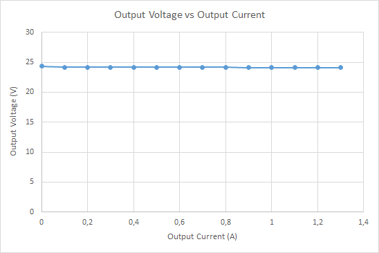
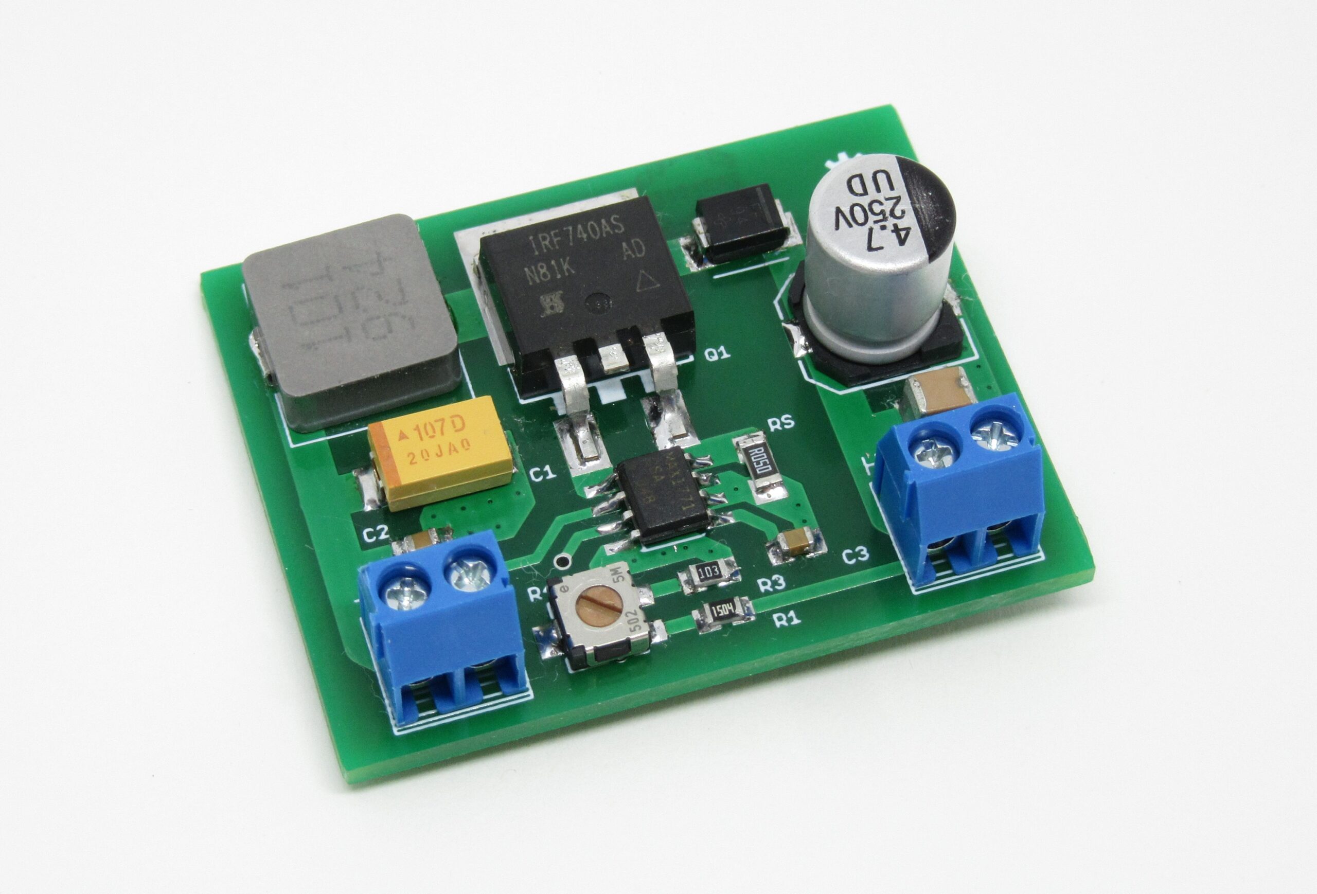
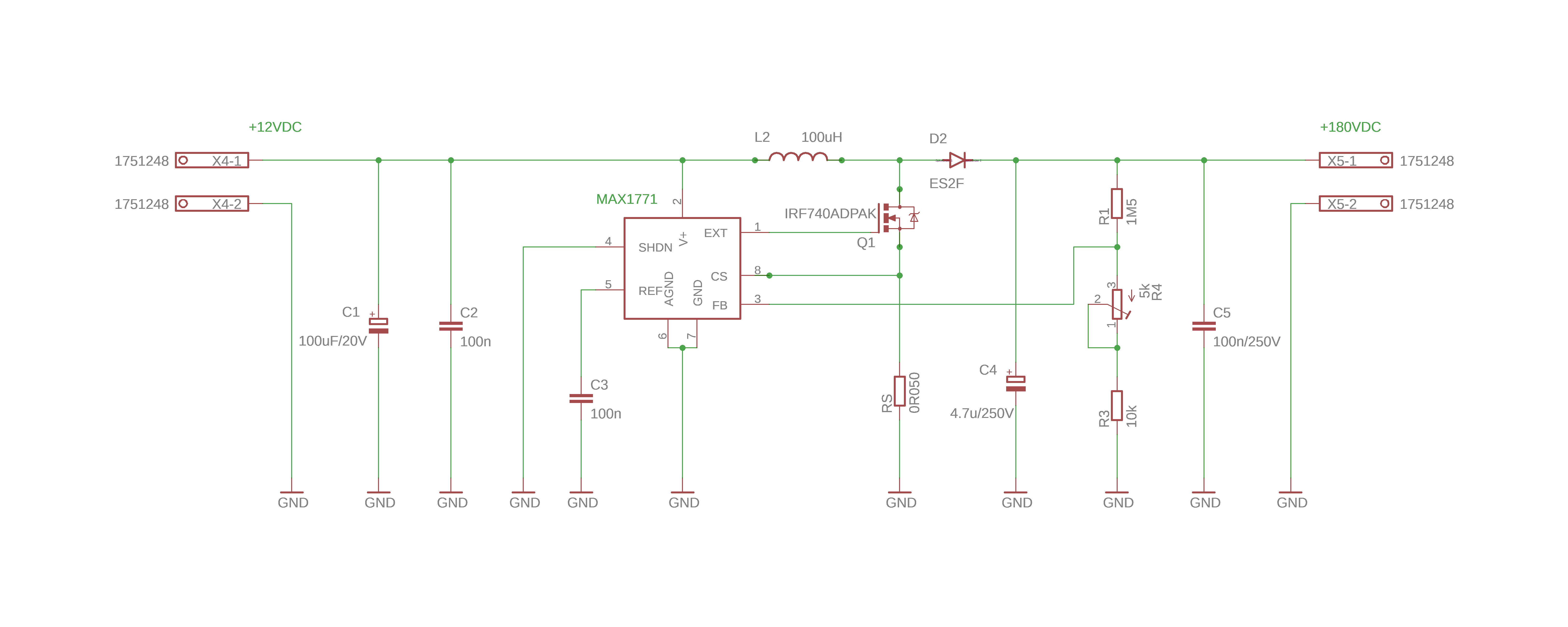
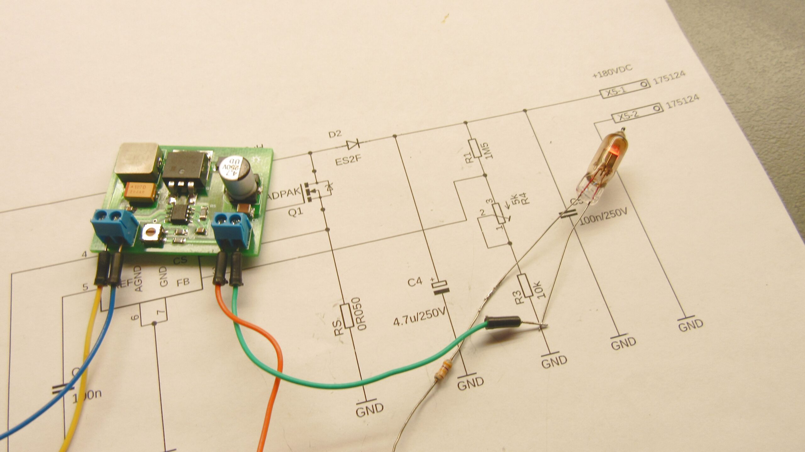
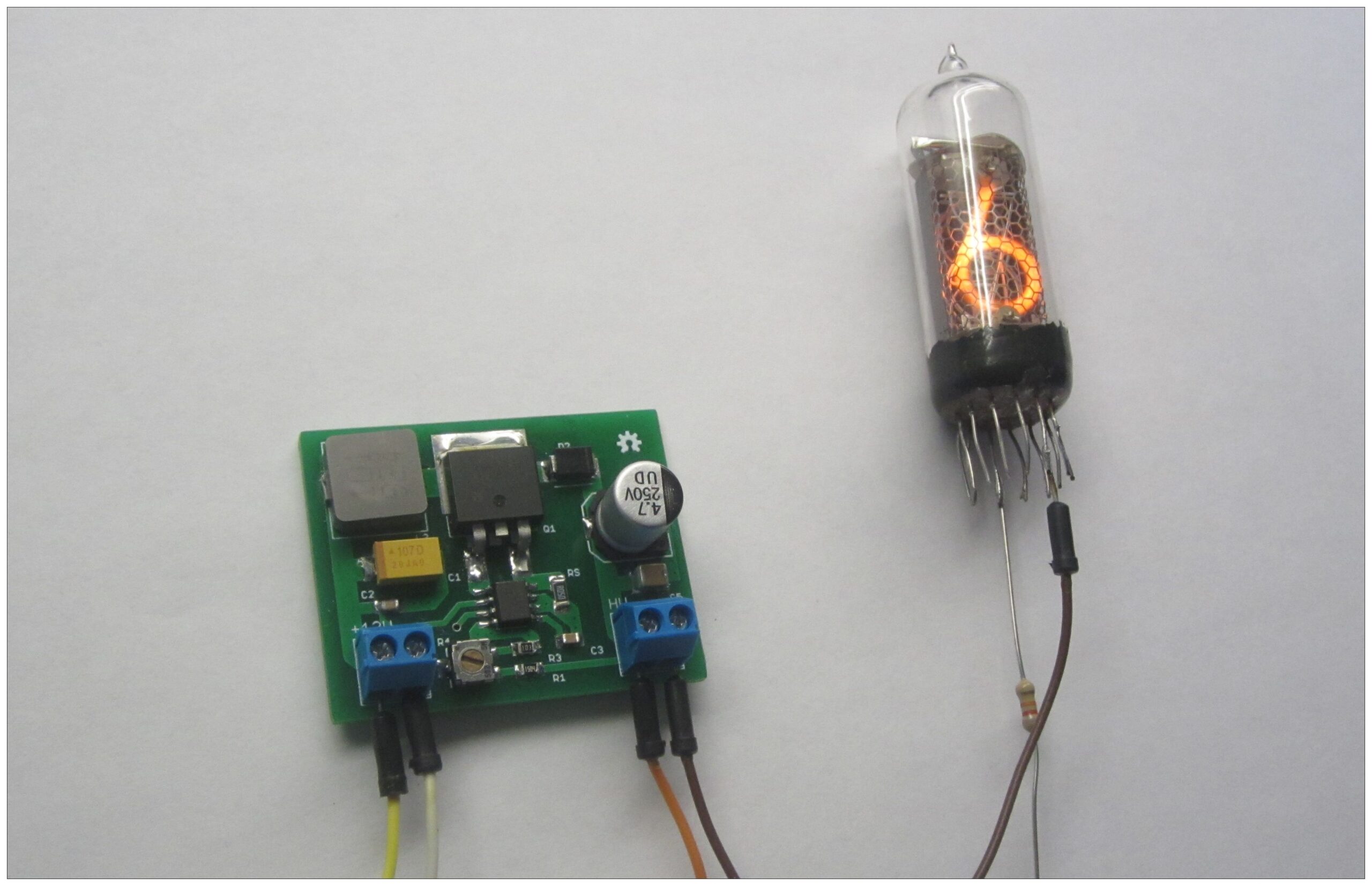
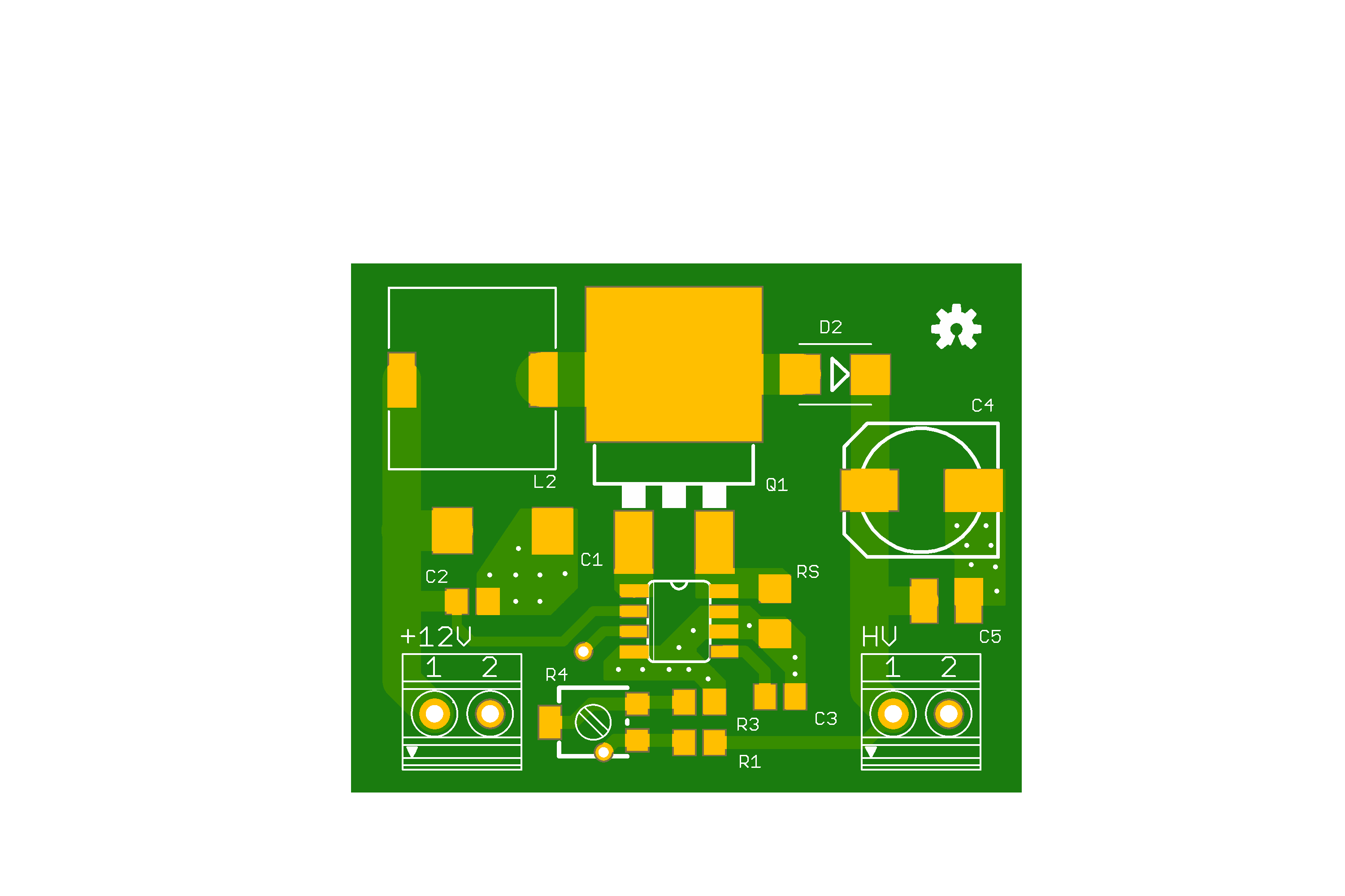
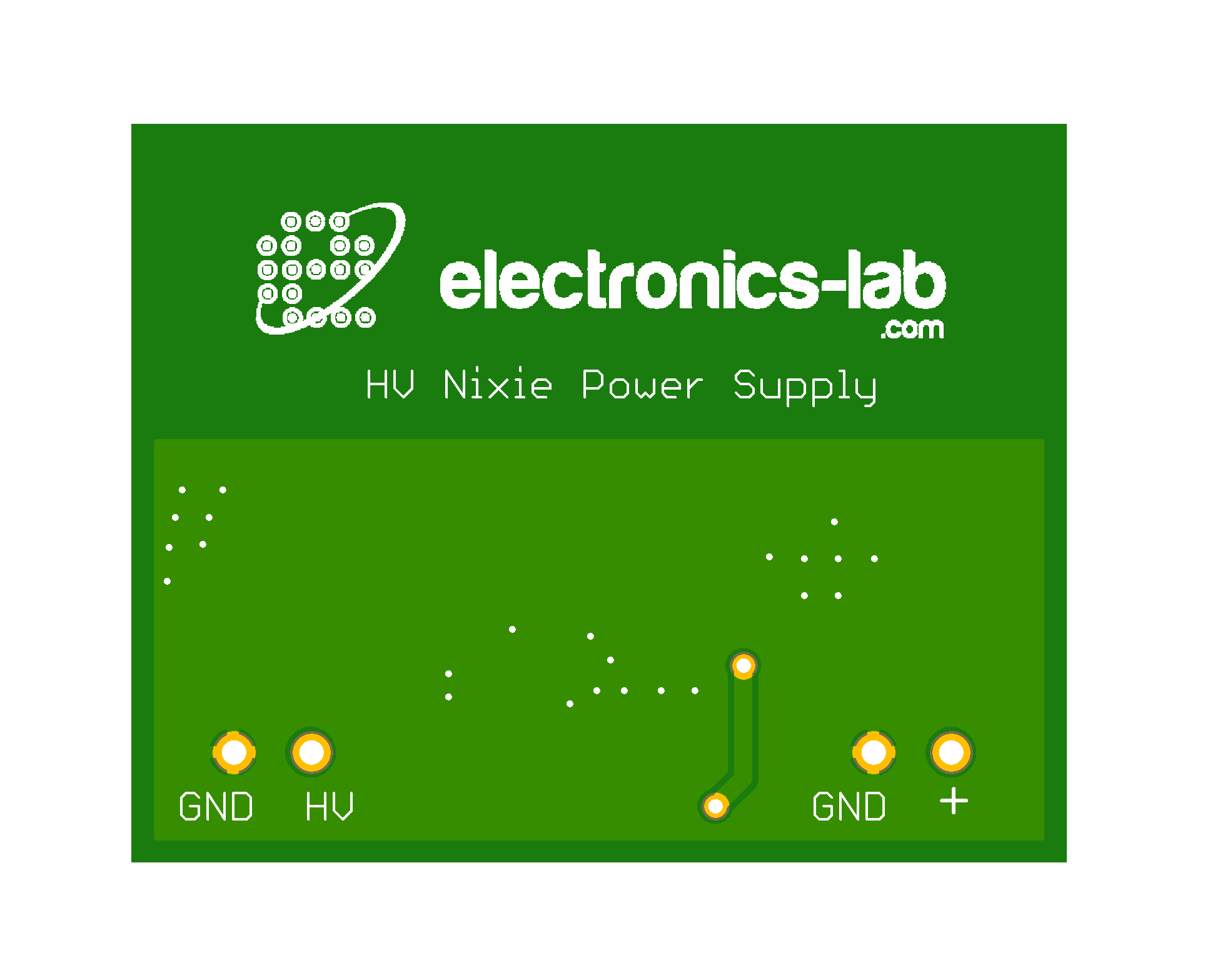
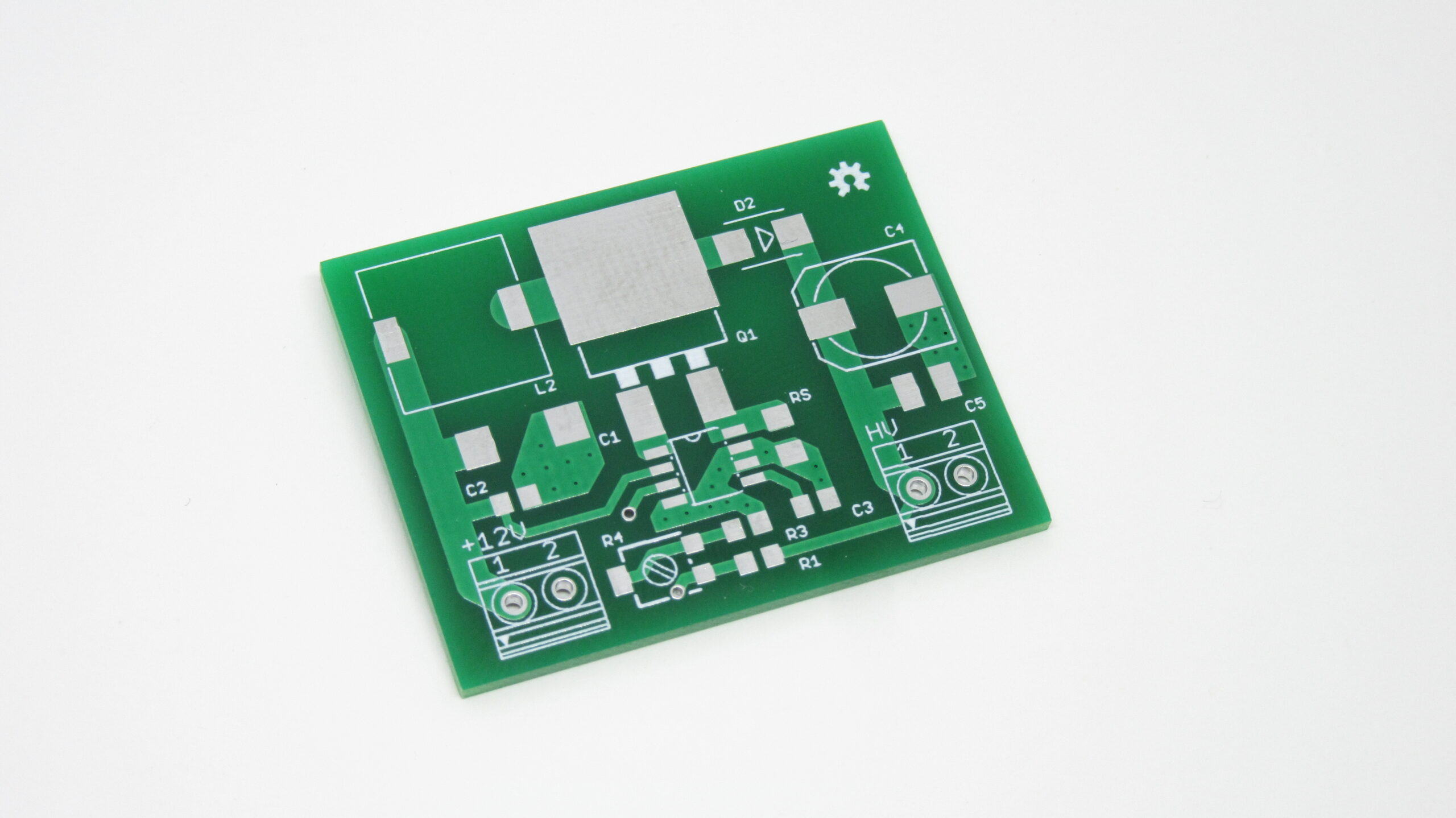
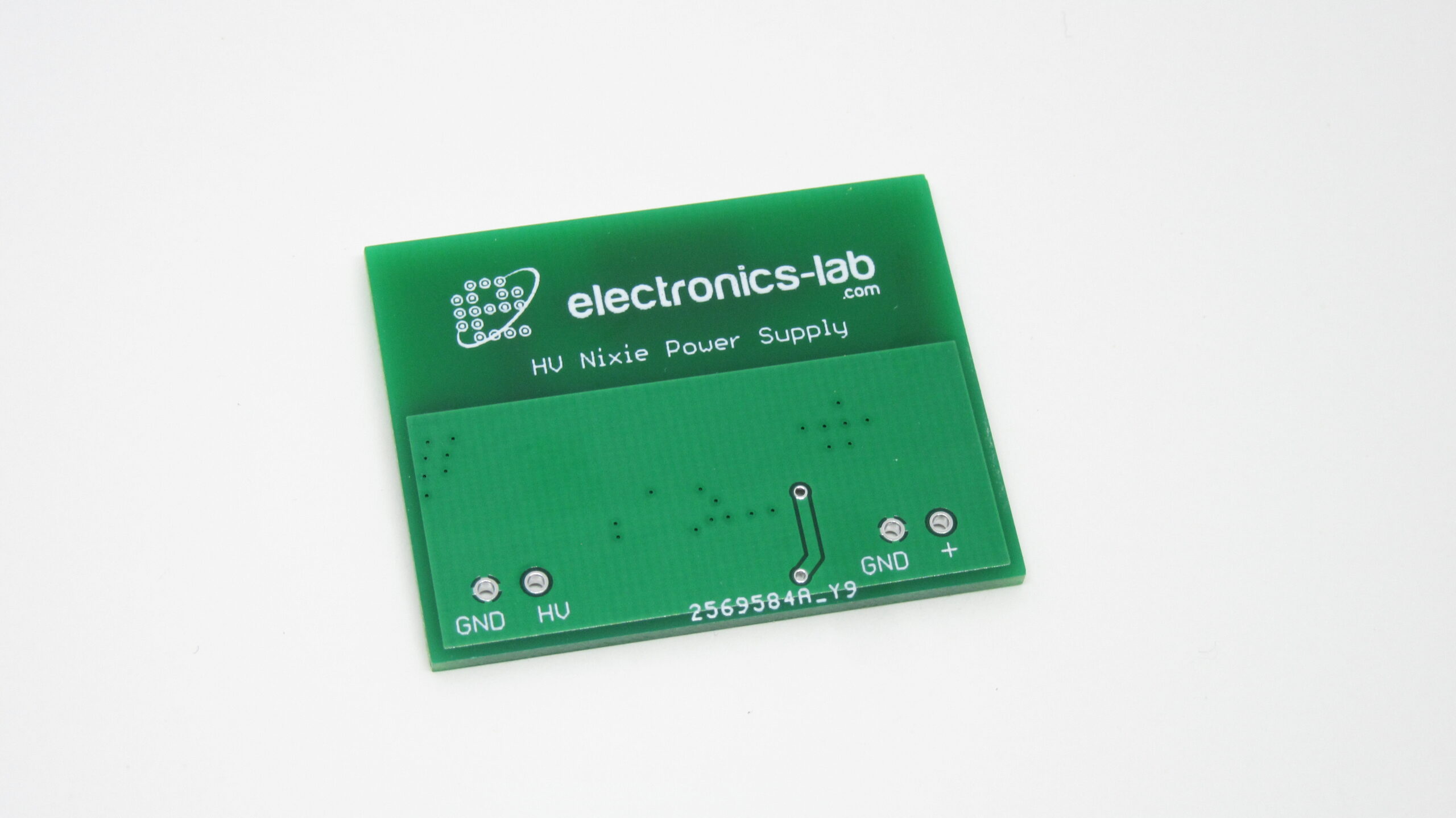
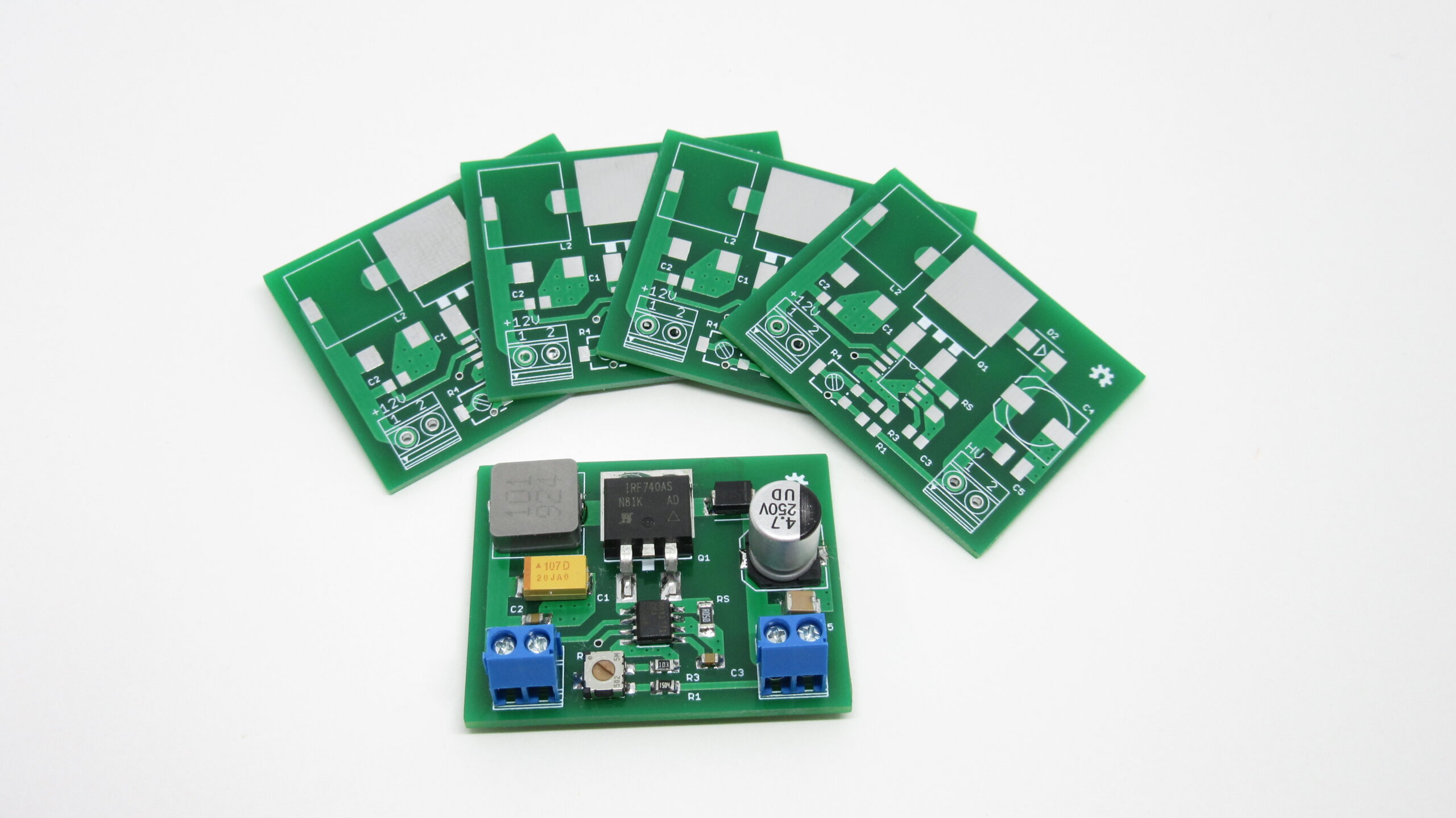
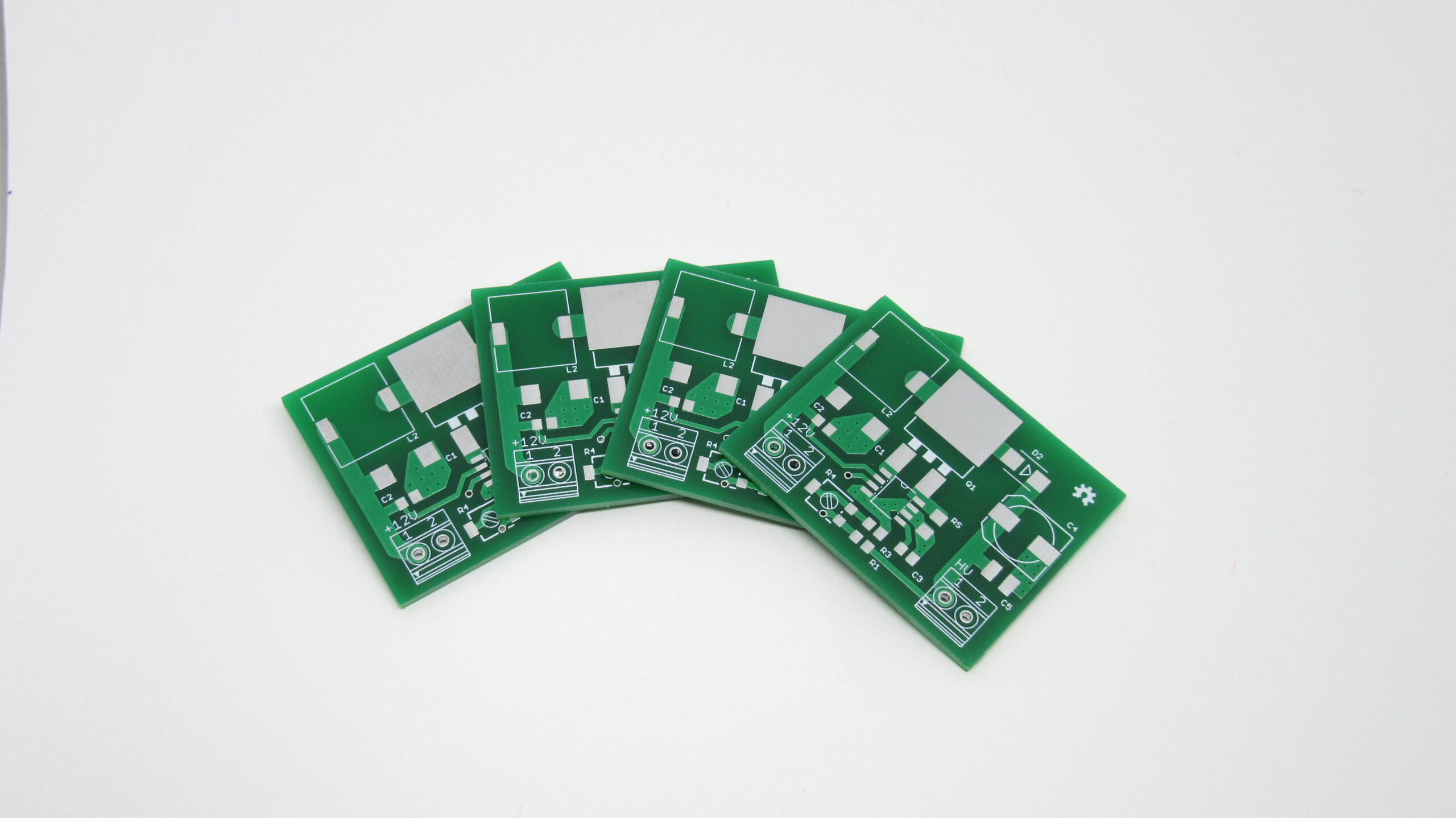
Nixie tubes need about ~180Vdc to light up and thus on most devices, a DC-DC converter is needed. Here we designed a simple DC-DC switching regulator capable of powering most of Nixie tubes. The board accepts 12Vdc input and gives an output of 150-250Vdc. The board is heavily inspired by Nick de Smith’s design.
Description
The module is based on the MAX1771 Step-Up DC-DC Controller. The controller works up to 300kHz switching frequency and that allows the usage of miniature surface mount components. In the default configuration, it accepts an input voltage from 2V to Vout and outputs 12V, but in this module, the output voltage is selected using the onboard potentiometer and it’s in the range 150-250Vdc. The maximum output current is 50mA @ 180Vdc.
The MAX1771 is driving an external N-channel MOSFET (IRF740) and with the help of the inductor and a fast diode, high voltage is produced.
MOSFET has to be low RDSon, the diode has to be fast Mttr, typically < 50nS, and capacitors have to be low ESR type to have good efficiency.
Precautions must be taken as this power supply uses high voltages. Build it only if you know what you are dealing with. Don’t touch any of the parts while in use.
Pay attention on the placement of C1 tantalum capacitor, as the bar indicates the anode (positive lead)
Schematic
Parts List
Part
Value
LCSC.com
R1
1.5M - 0805 SMD
C118025
R3
10k 0805
C269724
R4
5k trimmer SMD
C128557
Rs
0.05 Ohm - 0805 SMD
C149662
C1
100uF Tantalium SMD
C122302
C2, C3
100nF - 0805 SMD
C396718
C4
4.7uF / 250V SMD
C88702
C5
100nF / 250V SMD 1210
C52020
IC
MAX1771 SO-8
C407903
L1
100uH / 2.5 A
C2962892
Q1
IRF740 D2PAK (TO-263-2)
C39238
D2
ES2F-E3, ES2GB
C145321, C2844160
X1, X2
Screw Terminal - P=3.5mm
C474892
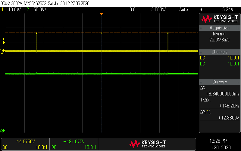
Oscilloscope Measurements
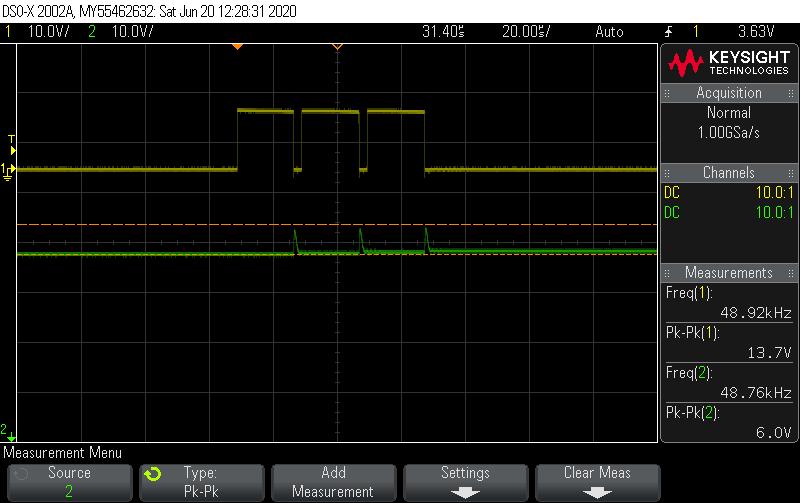
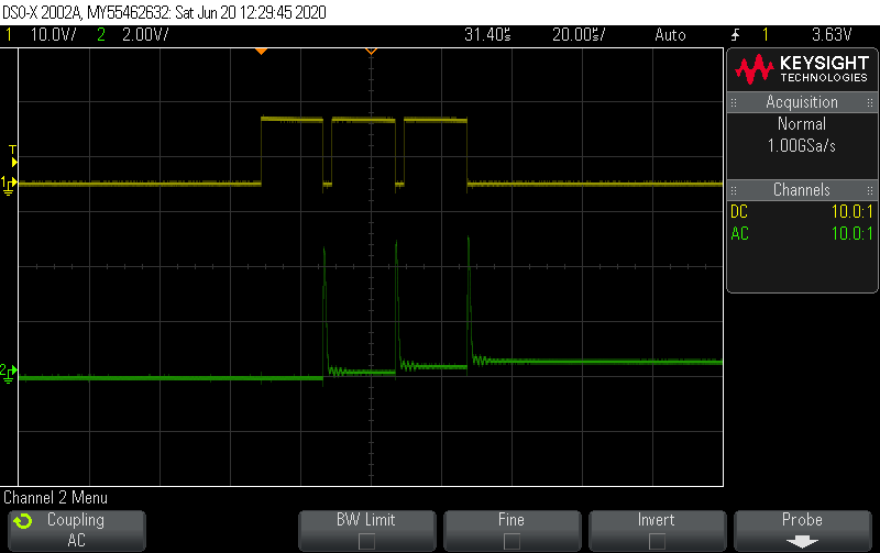
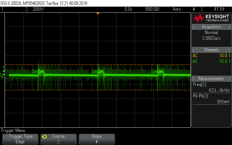
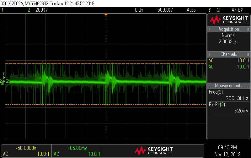
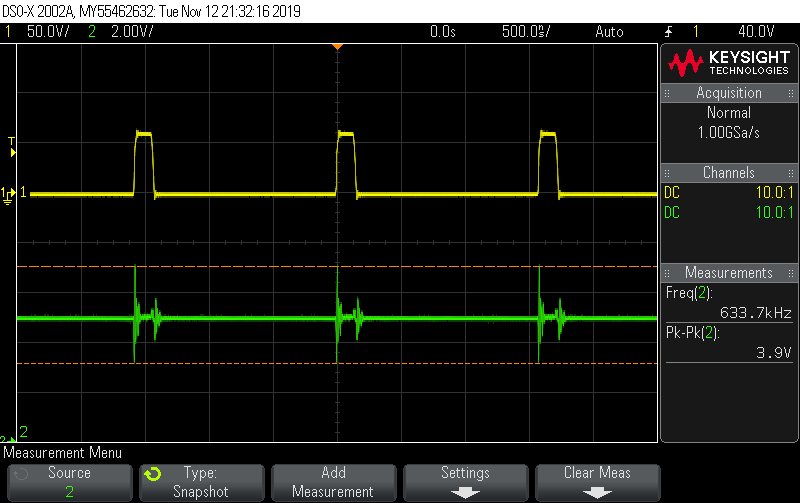
Yellow is the MOSFET Gate voltage and Green the output high voltage (~180Vdc). We see that the transistor switches with a low frequency of 146Hz and with a peak gate voltage of 12.8Vzoom in to the above short pulses reveals 3x pulses with 48.7Khz frequency to the gate of MOSFET. Also, the peak to peak ripple on output is 6Vfurther zoom to the output ripple reveals some short ringing and the peak ripple voltage.
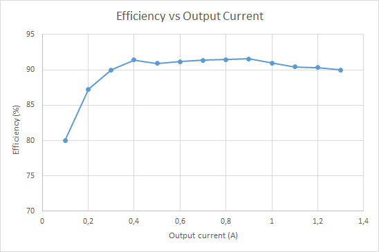
Efficiency
The module’s efficiency is calculated for two output currents (50mA and 25mA) at 180Vdc voltage output and 12V input. In the first case, the Pout = 8.1W while the Pin=10.96W, so efficiency is calculated at 73.9%. In the second case, the Pout = 4.1W while the Pin=5.52W, so efficiency is calculated at 74.2%. We see that for lower currents efficiency is a little greater than for the maximum current of 50mA.
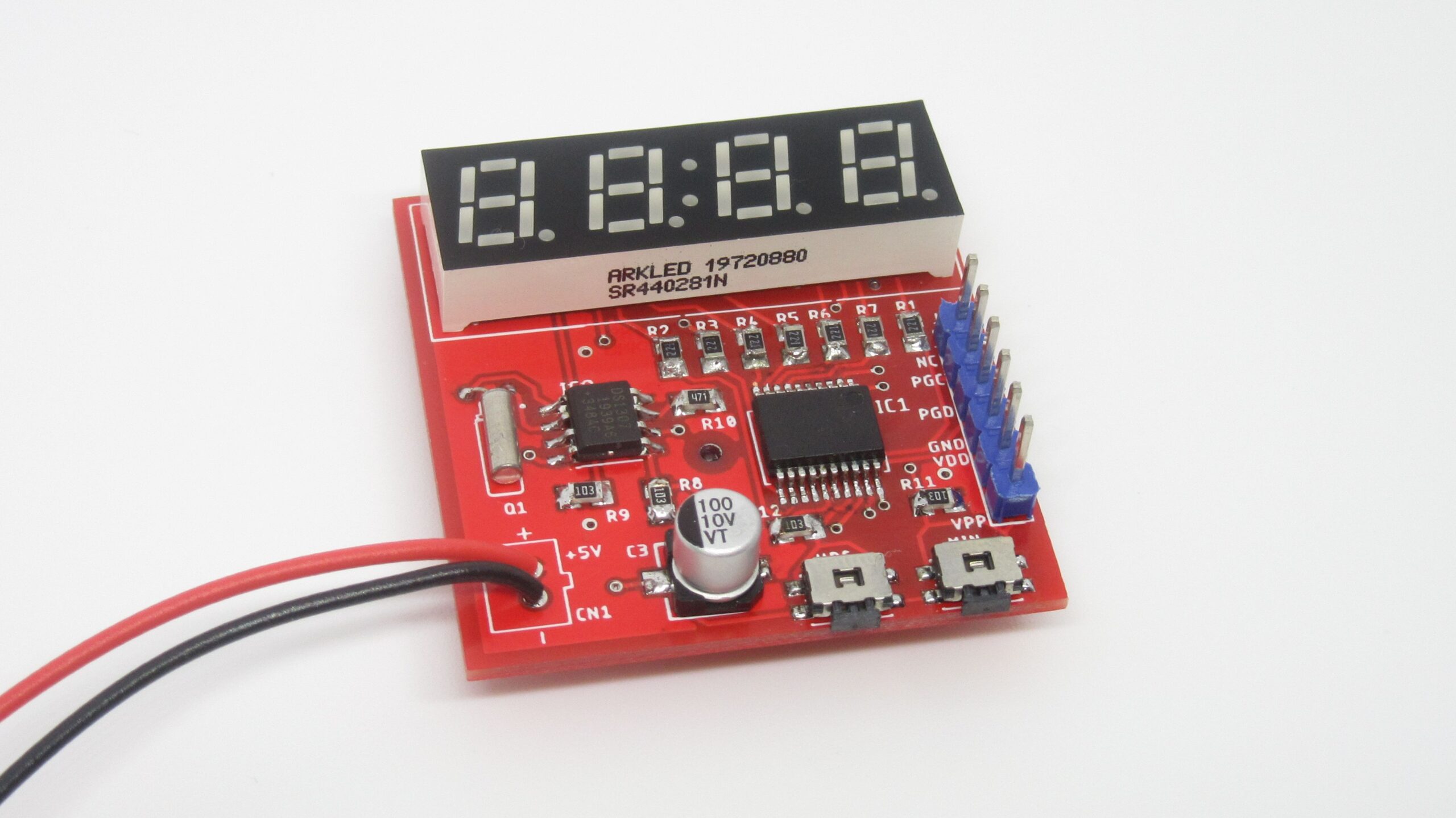
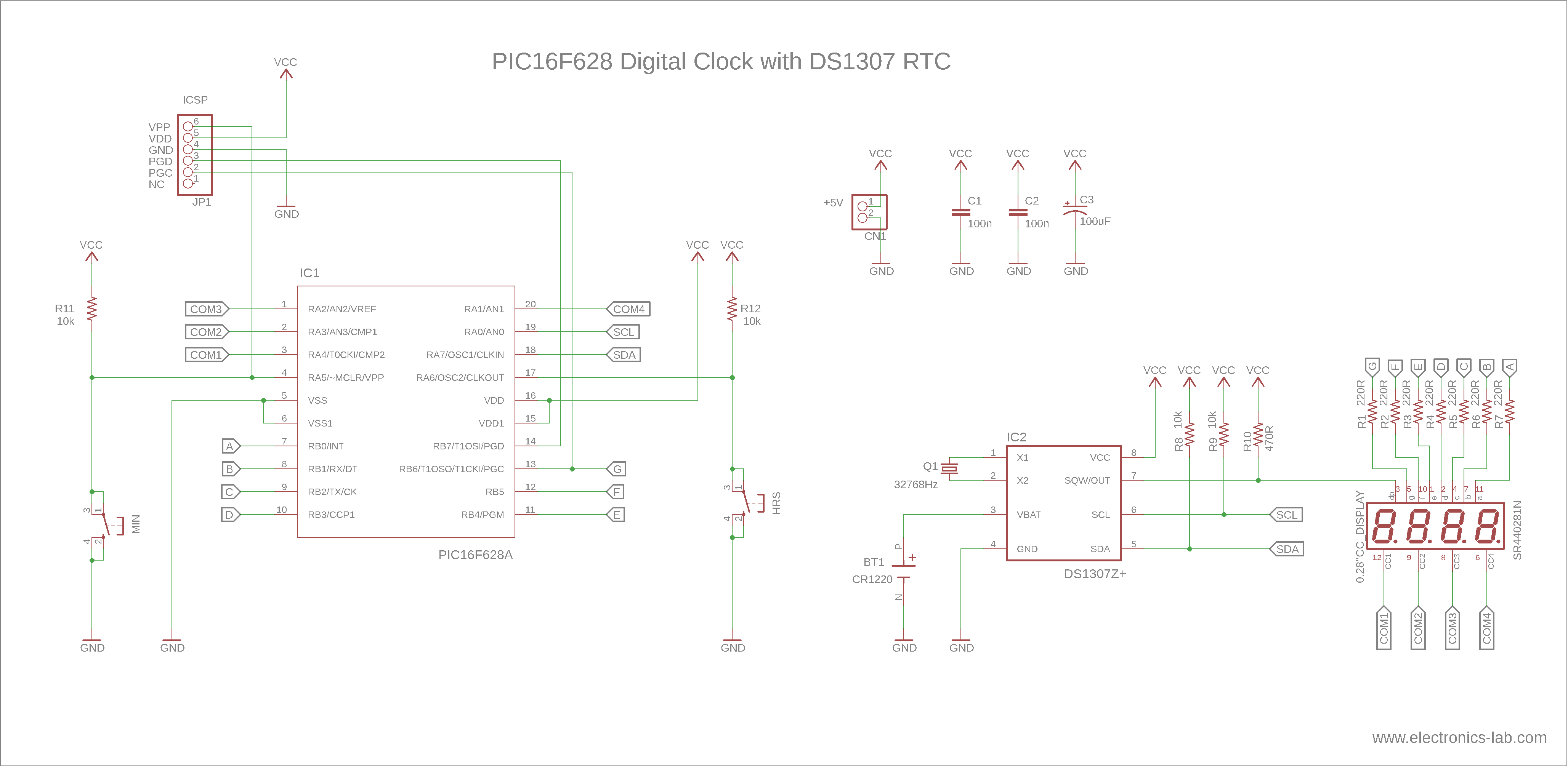
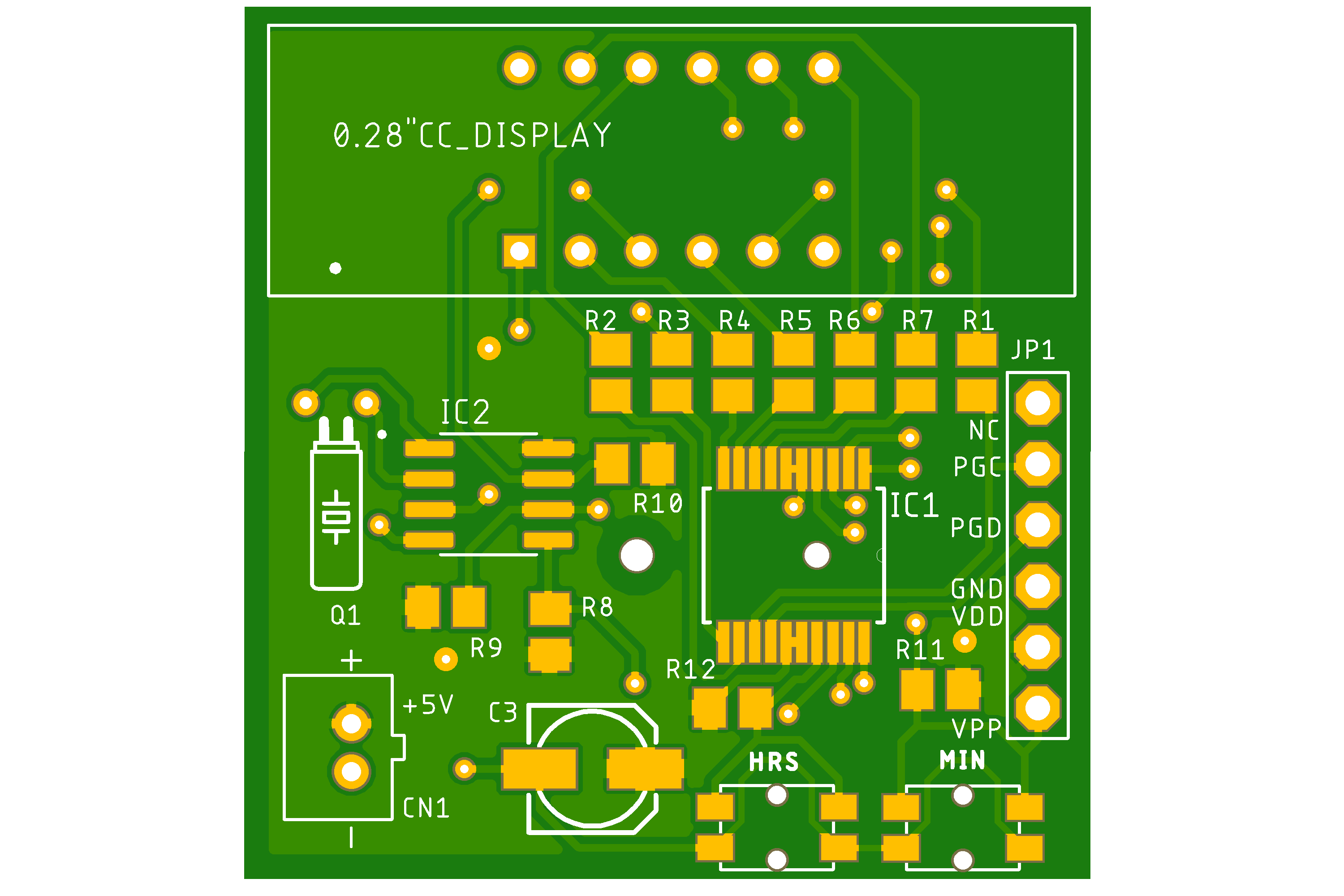
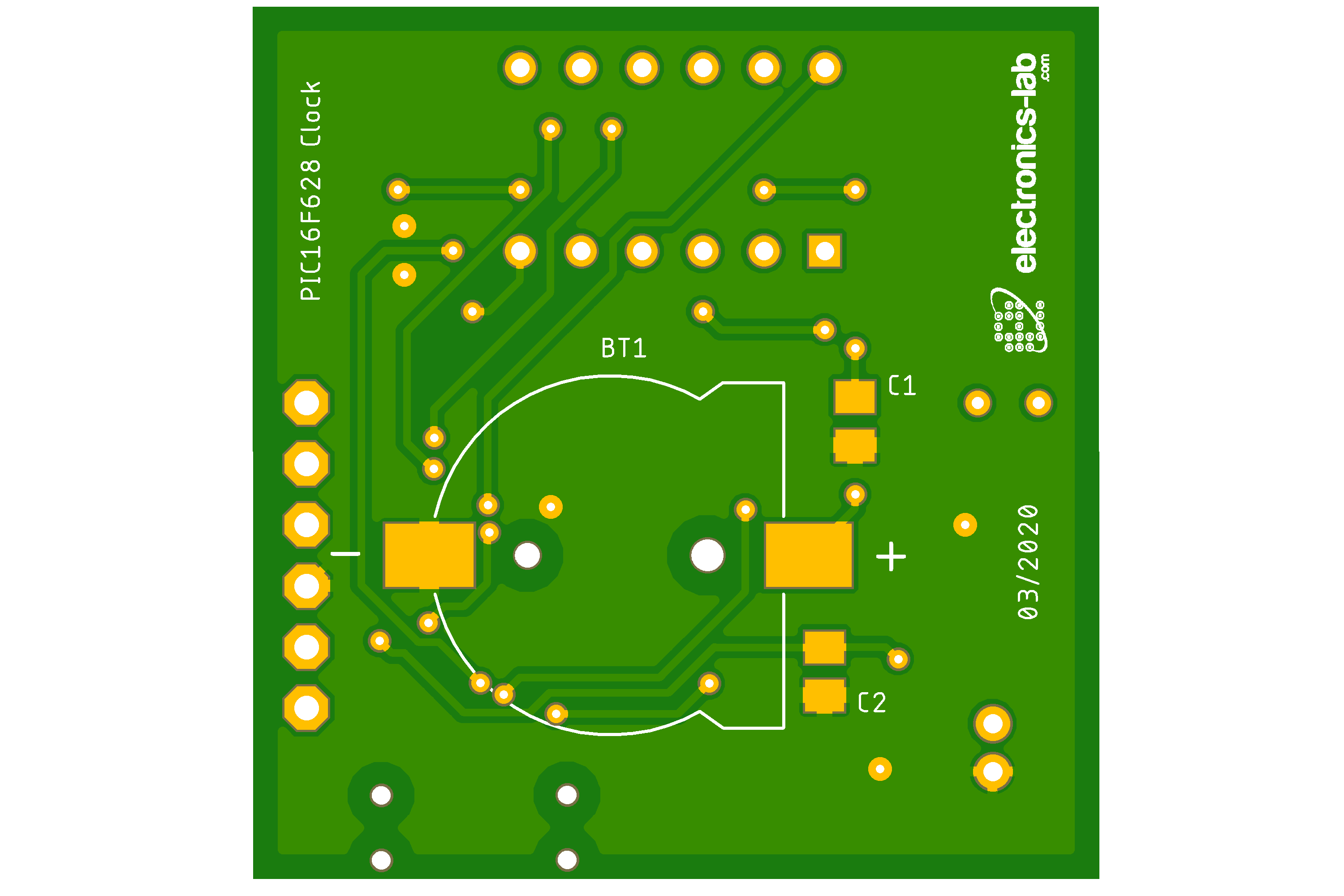
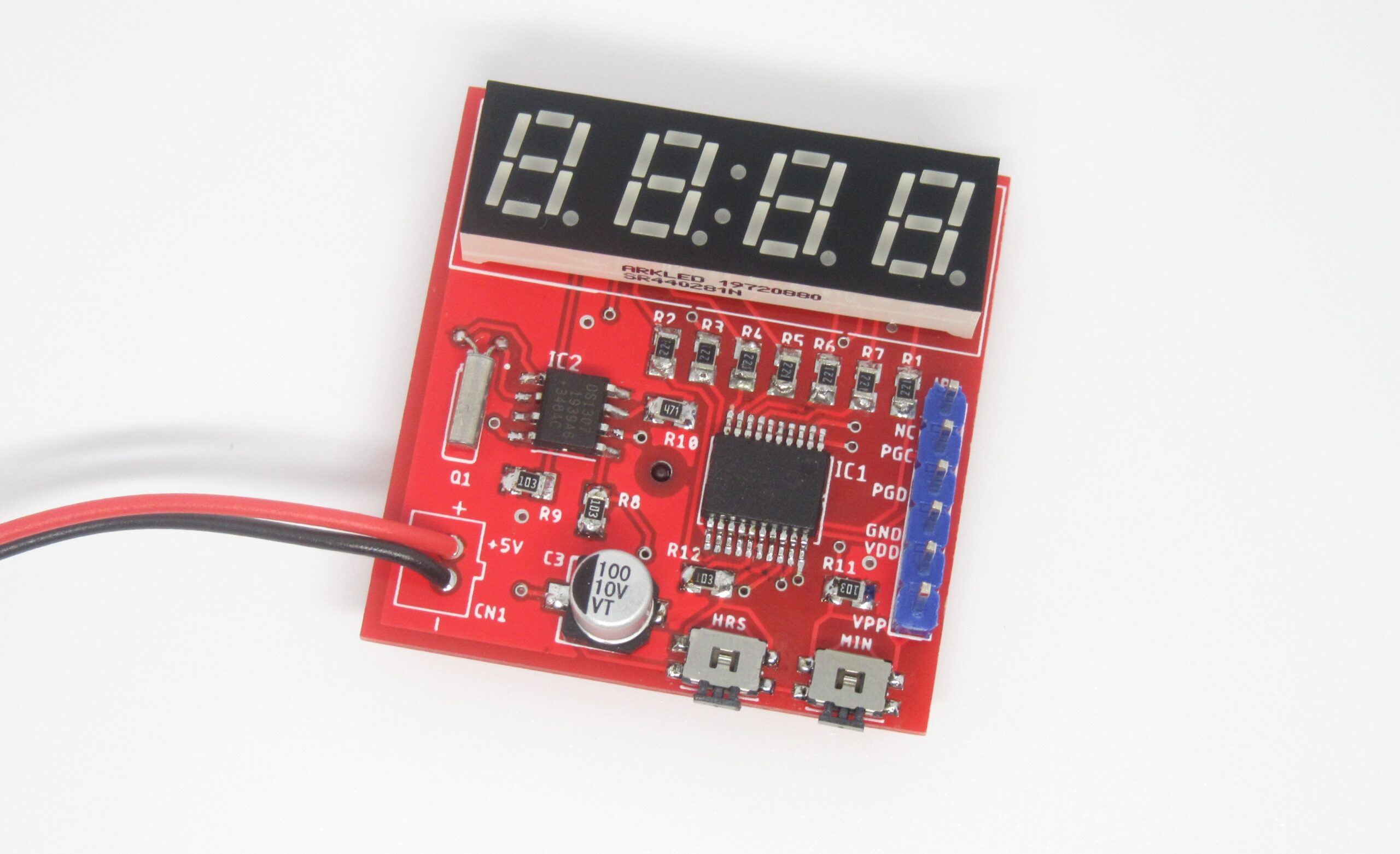
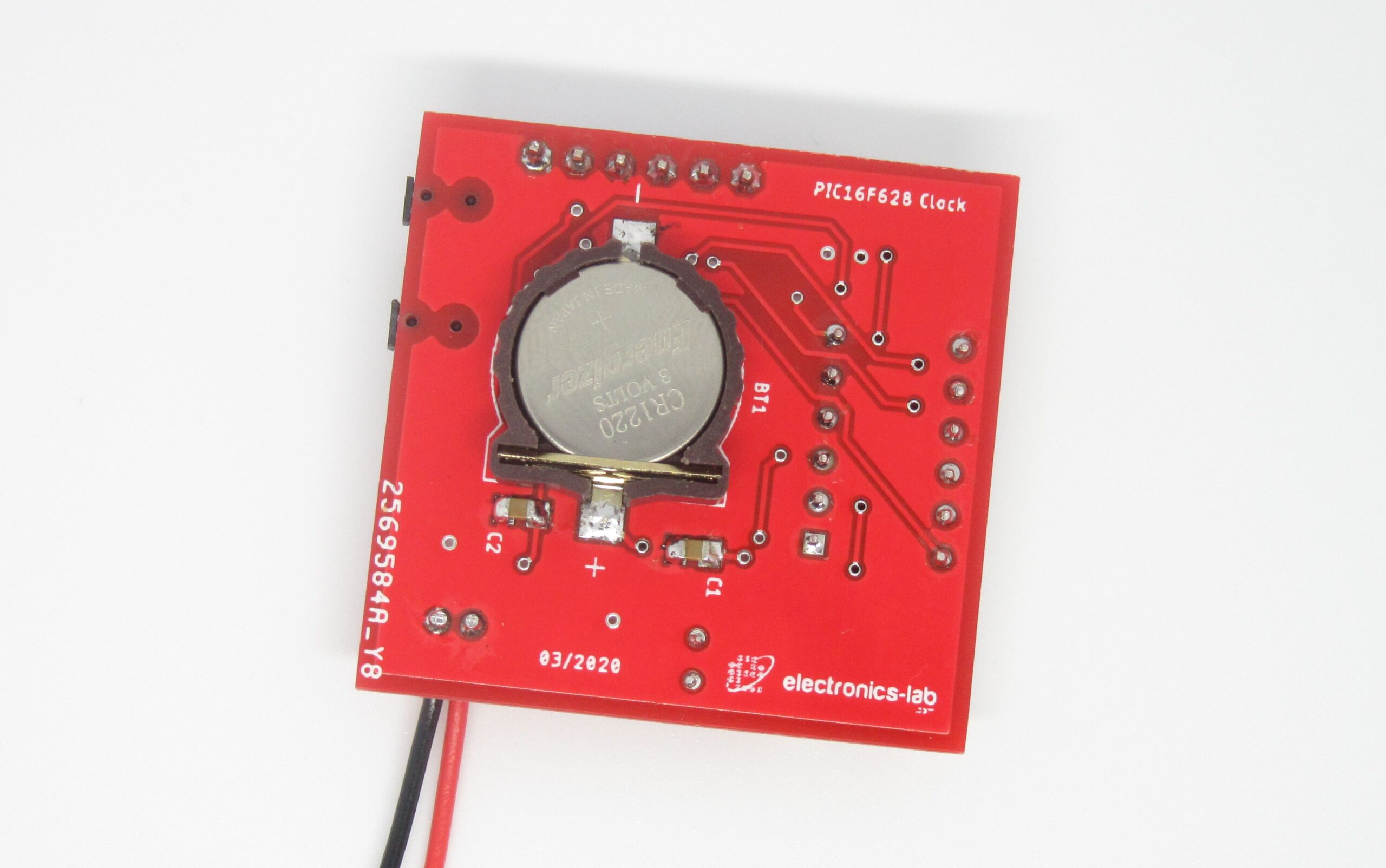
This is a minimal and small clock based on PIC16F628A microcontroller and DS1307 RTC IC. It is able to only show the time on a small 7-segment display with a total of 4 segments. The display we used is a 0.28″ SR440281N RED common cathode display bought from LCSC.com, but you can use other displays as well such as the 0.56″ Kingbright CC56-21SRWA. This project is heavily inspired by the “Simple Digital Clock with PIC16F628A and DS1307” in the case of schematic and we also used the same .hex as”Christo”.
Schematic
The schematic is straight forward. The heart is the PIC16F628A microcontroller running on the internal 4MHz oscillator, so no external crystal is needed. This saves us 2 additional IOs. The RESET Pin (MCLR) is also used as input for one of the buttons. All display segments are connected to PORTB and COMs are connected to PORTA. The RTC chip is also connected to PORTA using the I2C bus.
The refresh rate of the digits is about 53Hz and there is no visible flickering. The display segments are time-multiplexed and this makes them appear dimmer than the specifications. To compensate we are going to use some low resistors on the anodes. “Christo” tested it with different values for current limiting resistors R1-R7 and below 220Ω the microcontroller starts to misbehave (some of the digits start to flicker) above 220 Ohm everything seems OK. On the display we used the two middle dots are not connected to any pin on the package, so for the seconds’ indicators, we used the “comma” dots. These pins are connected to the SQW pin of the DS1307, which provides a square wave output with 1 sec period. The SQW pin is open drain, so we need to add a pull-up resistor. Τhe value of this resistor is chosen at 470Ω, after some trial and error testing. On the input side of the MCU, there are two buttons for adjusting the MINUTES and HOURS of the clock as indicated on the schematic. Onboard there is also an ICSP Programming connector, to help with the firmware upload. Finally, there is one unused pin left (RB7), which can be used for additional functionality, like adding a buzzer or an additional LED.
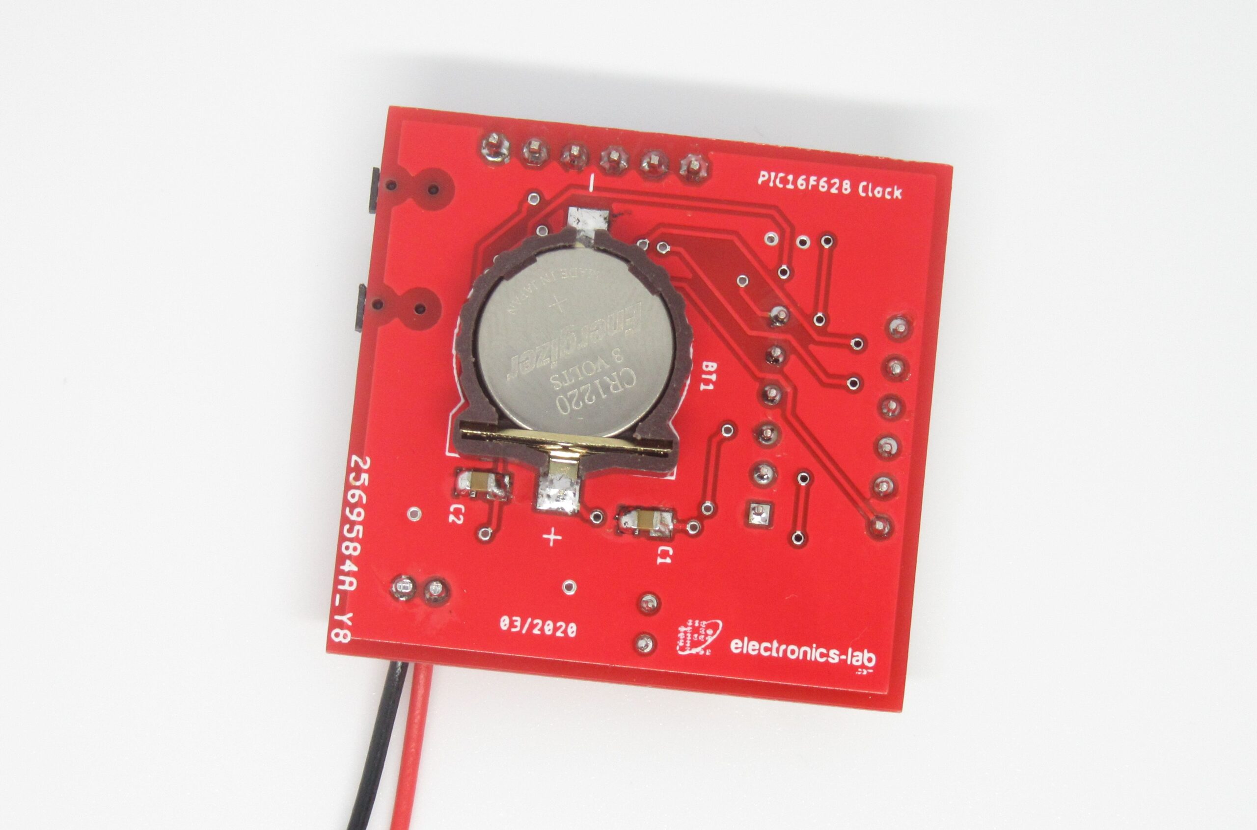
The DS1307 RTC needs an external crystal to keep the internal clock running and a backup battery to keep it running while the main power is OFF. So, the next time you power ON the clock the time would be current. To keep the overall board dimensions small we used a CR1220 battery holder with the appropriate 3V battery. Power consumption is about 35-40mA @ 5V input.
Code
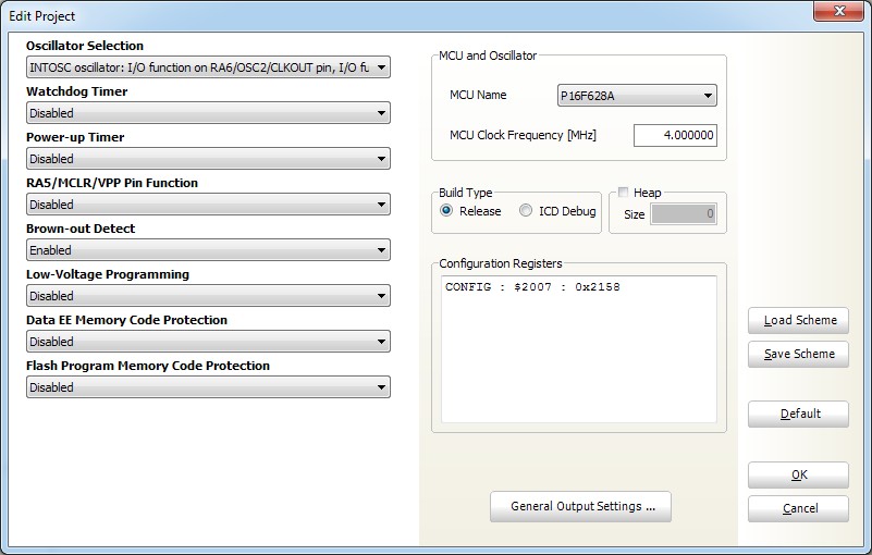
According to the author, the code is written and compiled with MikroC Pro and uses the build-in software I2C library for communicating with RTC chip. If you want to use MPLAB IDE for compiling the code you should write your own I2C library from scratch. For programming the board we used PICkit 3 programmer and software. In this case, in the “Tools” menu check the option “Use VPP First Program Entry“.
PIC Programmer Configuration
The code for this project is listed below. Additionally, you will need the “Digital Clock (PIC16F628A, DS1307, v2).h” file which can be found on the .zip in downloads below. Compiled .hex file is also provided on the same .zip file.
#include "Digital Clock (PIC16F628A, DS1307, v2).h"
#define b1 RA6_bit
#define b2 RA5_bit

// b1_old, b2_old - old state of button pins
// hour10, hour1 - tens and ones of the hour
// min10, min1 = tens and ones of the minutes
byte b1_old, b2_old, hour1, hour10, min1, min10;

// definitions for Software_I2C library
sbit Soft_I2C_Scl           at RA0_bit;
sbit Soft_I2C_Sda           at RA7_bit;
sbit Soft_I2C_Scl_Direction at TRISA0_bit;
sbit Soft_I2C_Sda_Direction at TRISA7_bit;


//  correct bits for each digit
//     RB6 RB5 RB4 RB3 RB2 RB1 RB0
//     g   f   e   d   c   b   a
//  0: 0   1   1   1   1   1   1   0x3F
//  1: 0   0   0   0   1   1   0   0x06
//  2: 1   0   1   1   0   1   1   0x5B
//  3: 1   0   0   1   1   1   1   0x4F
//  4: 1   1   0   0   1   1   0   0x66
//  5: 1   1   0   1   1   0   1   0x6D
//  6: 1   1   1   1   1   0   1   0x7D
//  7: 0   0   0   0   1   1   1   0x07
//  8: 1   1   1   1   1   1   1   0x7F
//  9: 1   1   0   1   1   1   1   0x6F
// BL: 0   0   0   0   0   0   0   0x00

const byte segments[11] = {0x3F, 0x06, 0x5B, 0x4F, 0x66, 0x6D, 0x7D, 0x07, 0x7F, 0x6F, 0x00};


//***********************************************//
//   Sets read or write mode at select address   //
//***********************************************//
void DS1307_Select(byte Read, byte address) {
     Soft_I2C_Start();
     Soft_I2C_Write(0xD0);       // start write mode
     Soft_I2C_Write(address);    // write the initial address
     if (Read) {
        Soft_I2C_Stop();
        Soft_I2C_Start();
        Soft_I2C_Write(0xD1);    // start read mode
     }
}

//********************************//
//   Initialize the DS1307 chip   //
//********************************//
void DS1307_Init() {
     byte sec, m, h;
     DS1307_Select(1, 0);                 // start reading at address 0
     sec = Soft_I2C_Read(1);              // read seconds byte
     m = Soft_I2C_Read(1);                // read minute byte
     h = Soft_I2C_Read(0);                // read hour byte
     Soft_I2C_Stop();
     if (sec > 127) {                     // if the clock is not running  (bit 7 == 1)
        DS1307_Select(0, 0);              // start writing at address 0
        Soft_I2C_Write(0);                // start the clock (bit 7 = 0)
        Soft_I2C_Stop();
        DS1307_Select(0, 7);              // start writing at address 7
        Soft_I2C_Write(0b00010000);       // enable square wave output 1 Hz
        Soft_I2C_Stop();
     }
     m = (m >> 4)*10 + (m & 0b00001111);  // converting from BCD format to decimal
     if (m > 59) {
        DS1307_Select(0, 1);              // start writing at address 1
        Soft_I2C_Write(0);                // reset the minutes to 0
        Soft_I2C_Stop();
     }
     if (h & 0b01000000) {                // if 12h mode (bit 6 == 1)
        if (h & 0b00100000)               // if PM (bit 5 == 1)
           h = 12 + ((h >> 4) & 1)*10 + (h & 0b00001111);
        else
           h = ((h >> 4) & 1)*10 + (h & 0b00001111);
     }
     else
        h = ((h >> 4) & 3)*10 + (h & 0b00001111);
     if (h > 23) {
        DS1307_Select(0, 2);              // start writing at address 2
        Soft_I2C_Write(0);                // reset the hours to 0 in 24h mode
        Soft_I2C_Stop();
     }
}


void incrementH() {     // increments hours and write it to DS1307
     hour1++;
     if ((hour10 < 2 && hour1 > 9) || (hour10 == 2 && hour1 > 3)) {
        hour1 = 0;
        hour10++;
        if (hour10 > 2)
           hour10 = 0;
     }
     DS1307_Select(0, 2);
     Soft_I2C_Write((hour10 << 4) + hour1);
     Soft_I2C_Stop();
}


void incrementM() {     // increments minutes and write it to DS1307
     min1++;
     if (min1 > 9) {
        min1 = 0;
        min10++;
        if (min10 > 5)
           min10 = 0;
     }
     DS1307_Select(0, 0);
     Soft_I2C_Write(0);                       // reset seconds to 0
     Soft_I2C_Write((min10 << 4) + min1);     // write minutes
     Soft_I2C_Stop();
}

void main(){
     // pos: current digit position;
     // counter1, counter2: used as flag and for repeat functionality for the buttons
     // COM[]: drive the common pins for the LED display
     byte pos, counter1, counter2, COM[4] = {0b11101111, 0b11110111, 0b11111011, 0b11111101};
     CMCON = 0b00000111;             // comparator off
     TRISA = 0b01100000;
     TRISB = 0b00000000;
     b1_old = 1;
     b2_old = 1;
     counter1 = 0;
     counter2 = 0;
     pos = 0;
     Soft_I2C_Init();
     DS1307_Init();
     while (1) {
           DS1307_Select(1, 1);      // select reading at address 1
           min1 = Soft_I2C_Read(1);  // read minutes byte
           hour1 = Soft_I2C_Read(0); // read houts byte
           Soft_I2C_Stop();
           min10 = min1 >> 4;
           min1 = min1 & 0b00001111;
           hour10 = hour1 >> 4;
           hour1 = hour1 & 0b00001111;
           if (b1 != b1_old) {        // if the button1 is pressed or released
              b1_old = b1;
              counter1 = 0;
           }
           if (!b1_old) {             // if the button1 is pressed
              if (counter1 == 0)
                 incrementH();        // increment hour
              counter1++;
              if (counter1 > 50)      // this is repeat functionality for the button1
                 counter1 = 0;
           }
           if (b2 != b2_old) {        // if the button2 is pressed or released
              b2_old = b2;
              counter2 = 0;
           }
           if (!b2_old) {             // if the button2 is pressed
              if (counter2 == 0)
                 incrementM();        // increment minutes and reset the seconds to 0
              counter2++;
              if (counter2 > 50)      // this is repeat functionality for the button2
                 counter2 = 0;
           }

           TRISA = TRISA | 0b00011110;       // set all 4 pins as inputs
           switch (pos) {                    // set proper segments high
             case 0: PORTB = segments[hour10]; break;
             case 1: PORTB = segments[hour1]; break;
             case 2: PORTB = segments[min10]; break;
             case 3: PORTB = segments[min1]; break;
           }
           TRISA = TRISA & COM[pos];         // set pin at current position as output
           PORTA = PORTA & COM[pos];         // set pin at current position low
           pos++;                            // move to next position
           if (pos > 3) pos = 0;
     }
}
PCB
PCB is designed with Autodesk EAGLE and design files are available in downloads below. The overall dimensions of the board are 35.56 x 36.61 mm and we used almost SMD components.
Spare PCBs are available for shipment around the world. If you would like to get some drop us a line.
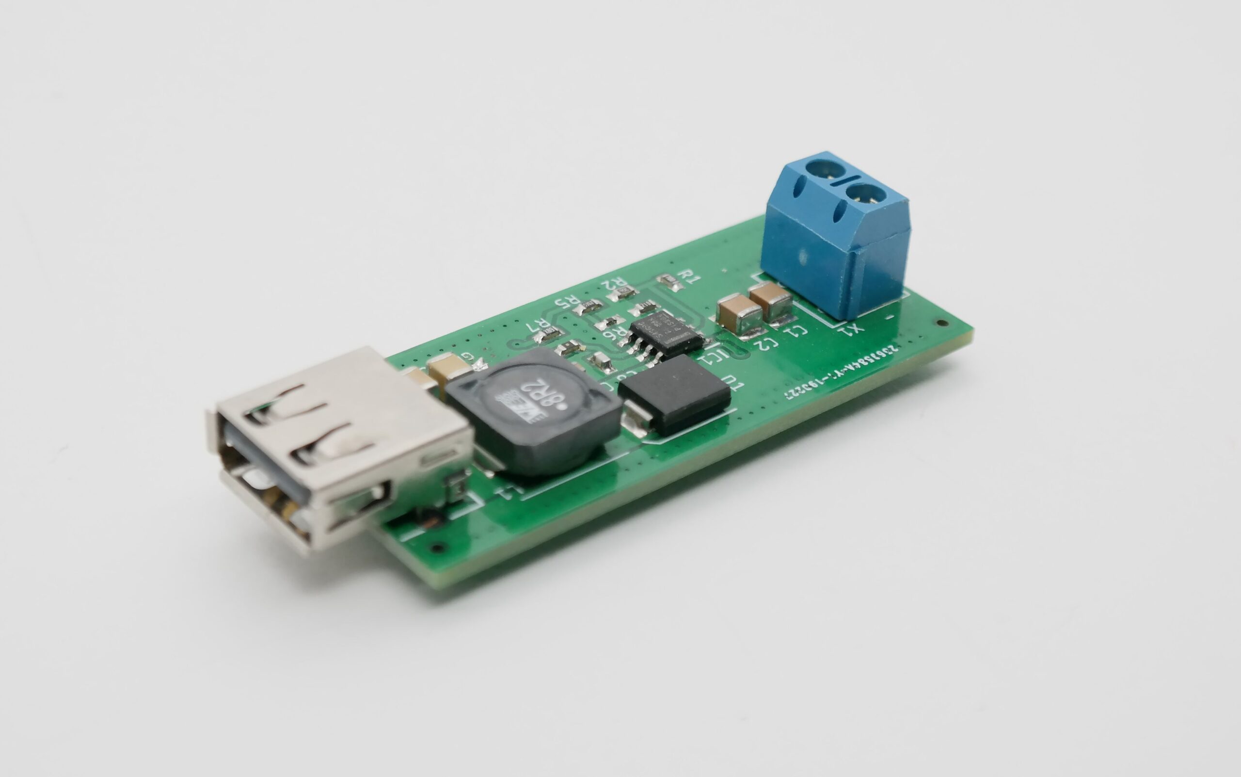
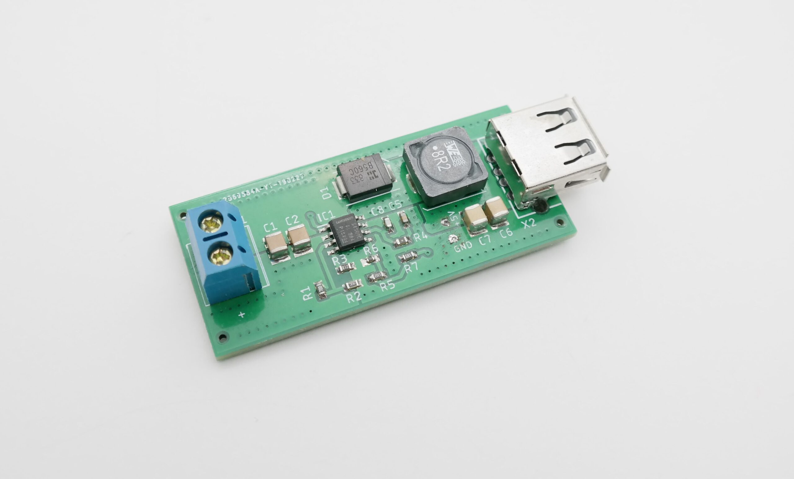
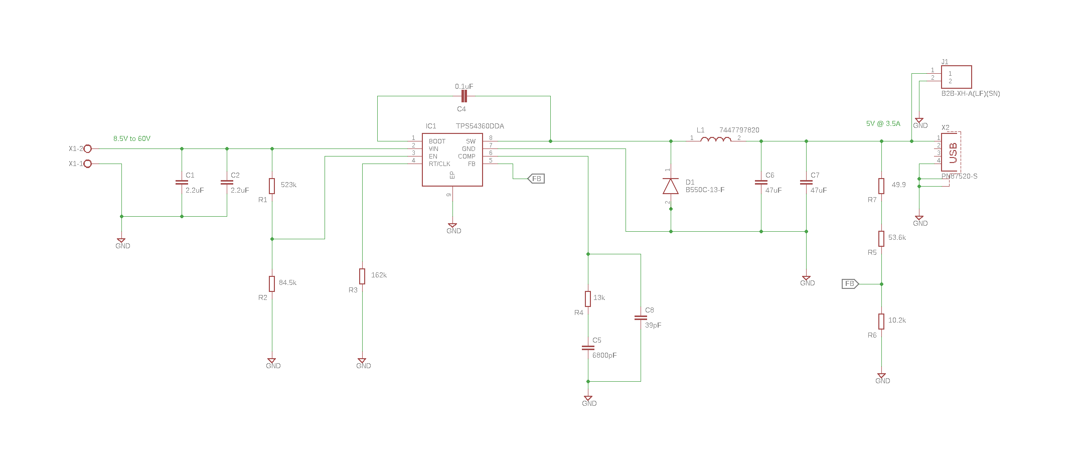
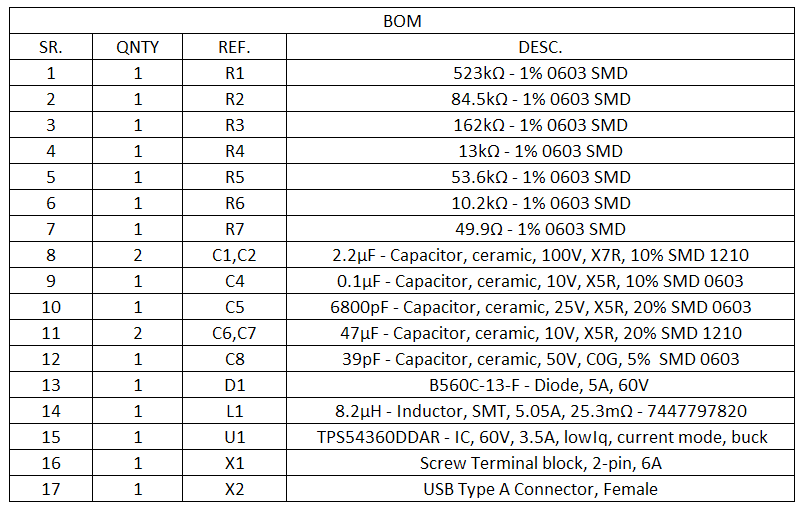
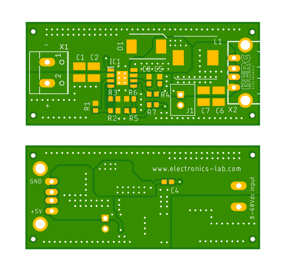
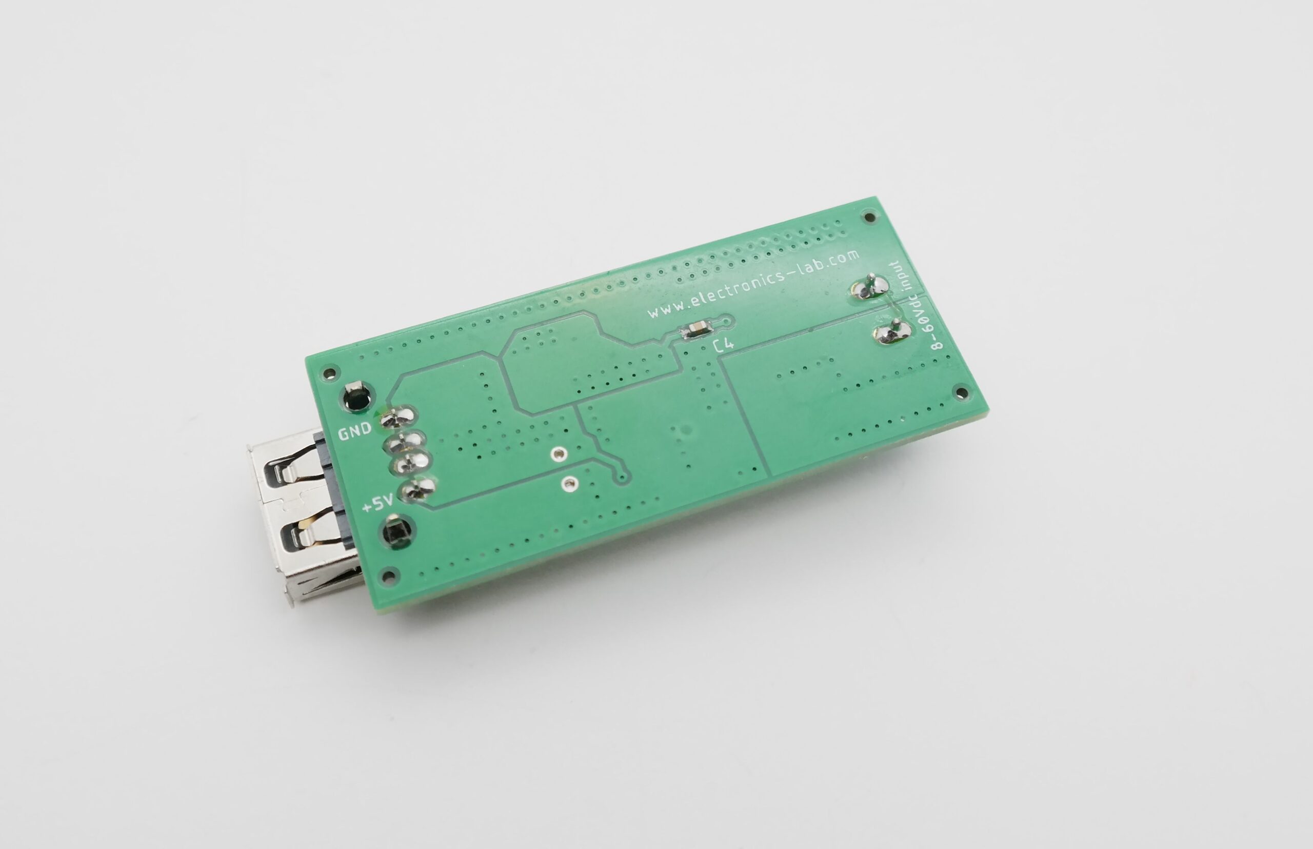
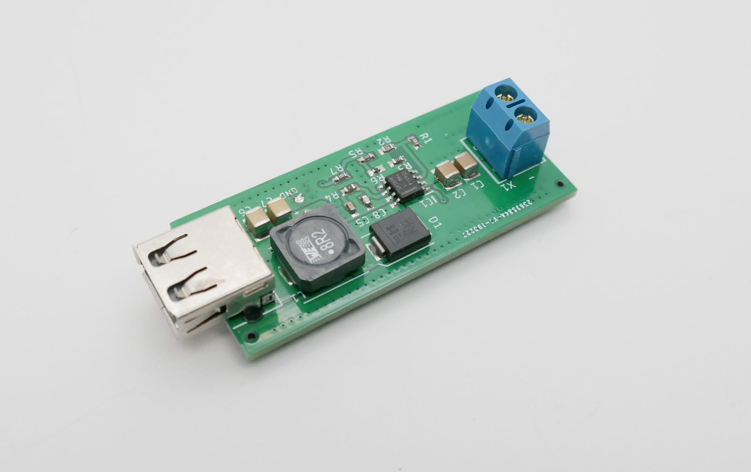
This is a 60V to 5V – 3.5A step down DC-DC converter based on TPS54360B from Texas Instruments. Sample applications are: 12 V, 24 V and 48 V industrial, Automotive and Communications Power Systems. The TPS54360 is a 60V, 3.5A, step down regulator with an integrated high side MOSFET. The device survives load dump pulses up to 65V per ISO 7637. Current mode control provides simple external compensation and flexible component selection. A low ripple pulse skip mode reduces the no load supply current to 146 μA. Shutdown supply current is reduced to 2 μA when the enable pin is pulled low.
Under-voltage lockout is internally set at 4.3 V but can be increased using the enable pin. The output voltage start up ramp is internally controlled to provide a controlled start up and eliminate overshoot. A wide switching frequency range allows either efficiency or external component size to be optimized. Frequency fold back and thermal shutdown protects internal and external components during an overload condition.
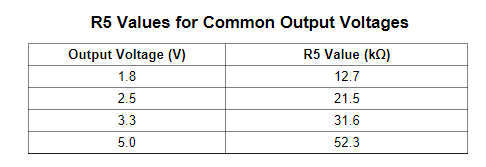
Note: The output voltage is set by a resistor divider from the output node to the FB terminal. It is recommended to use 1% tolerance or better divider resistors, choose R5, R6 for other output voltages.
It is strongly recommended to use adequate air flow over the board to ensure it doesn’t go at thermal shutdown. See thermal profile below.
Setting Output Voltage
The following table lists the R5 values for some common output voltages assuming R6= 10.0kΩ
Features
Supply Input 8.5V-60V
Output 5V (Output Voltage adjustable with R5, R6)
Output Current 3.5A
100 kHz to 2.5 MHz Switching Frequency
Optional JST connector for 5V Fan
Current Mode Control DC-DC Converter
Integrated 90-mΩ High Side N-Channel MOSFET
High Efficiency at Light Loads with Pulse Skipping Eco-mode™
Low Dropout at Light Loads with Integrated BOOT Recharge FET
146 μA Operating Quiescent Current
1 µA Shutdown Current
Internal Soft-Start
Accurate Cycle-by-Cycle Current Limit
Thermal, Overvoltage, and Frequency Fold back Protection
PCB Dimensions 55.50mm x 24.64mm
Schematic
Parts List
PCB
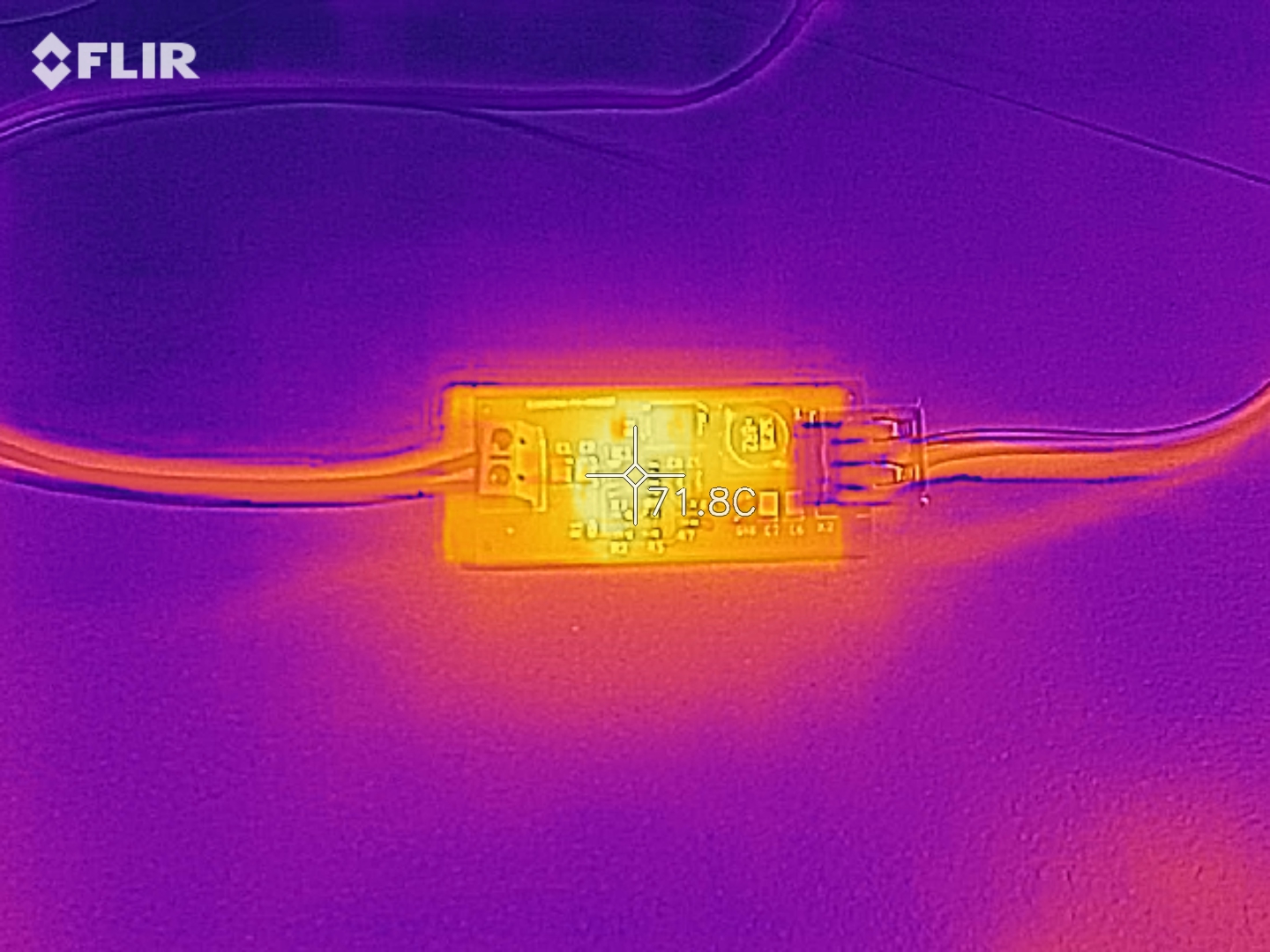
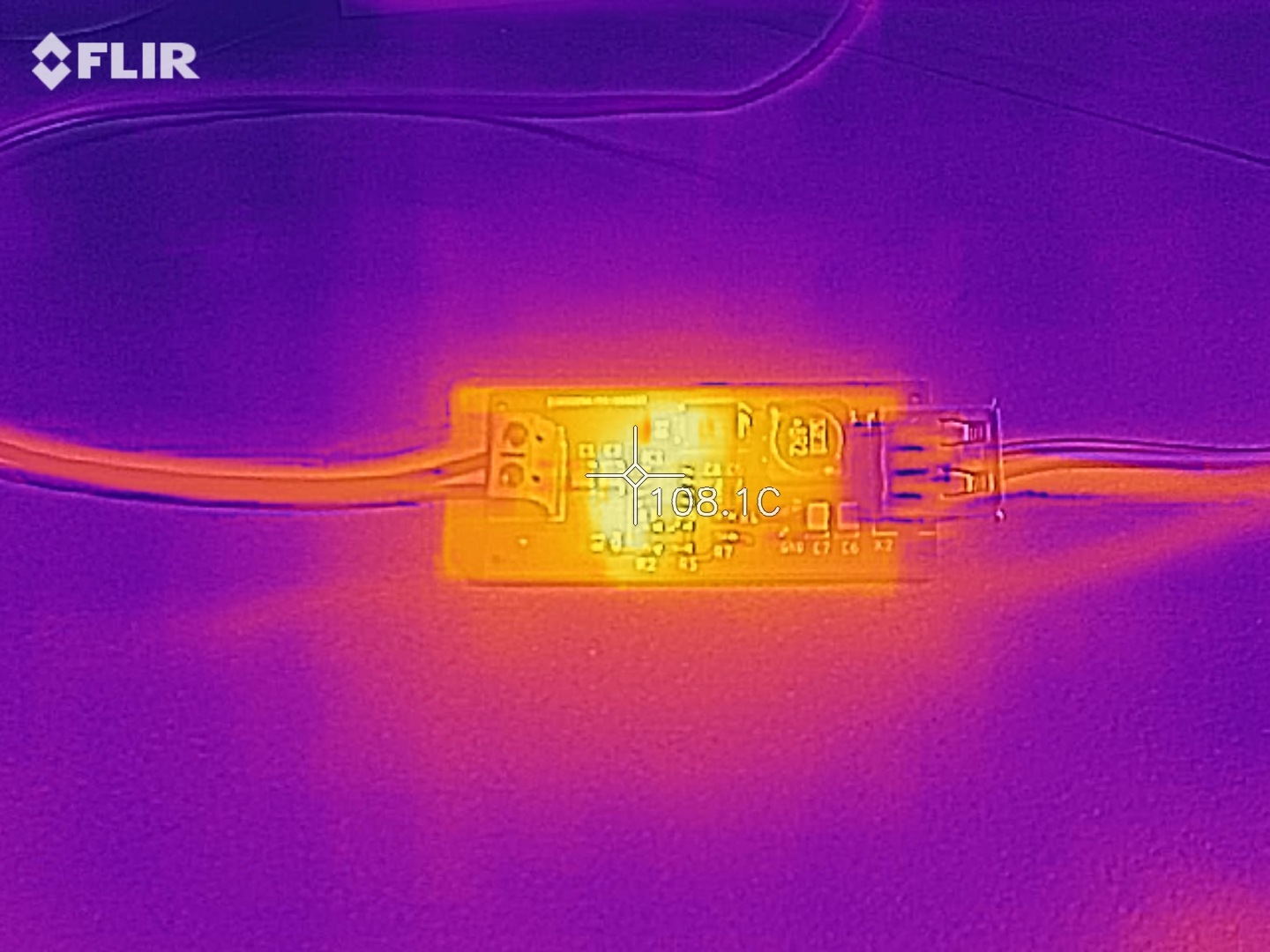
Thermal Image
You can see on the thermal images below that at 60V input – 5V @2A output the IC gets too hot (>105ºC) and if we go for higher outputs (2.5-3A) the IC gets in thermal cut-off. To avoid this situation you can use a small 5V FAN to blow air on the board or probably use a heatsink attached to the board.
60V input – 5V @1A output60V input – 5V @2A output60V input – 5V @3A output cooled with a small FAN
Measurements
The efficiency is calculated based on the (Pout/Pin)*100%. For 60V input and 5V @3A output the input current is 0.32A, so Pin=19.38W. Pout=5V*3A=15W, so e=77.39% with Pdis = 4.58W
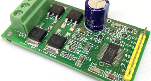
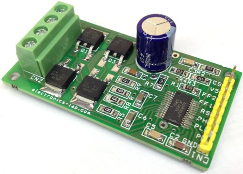
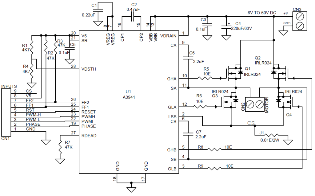
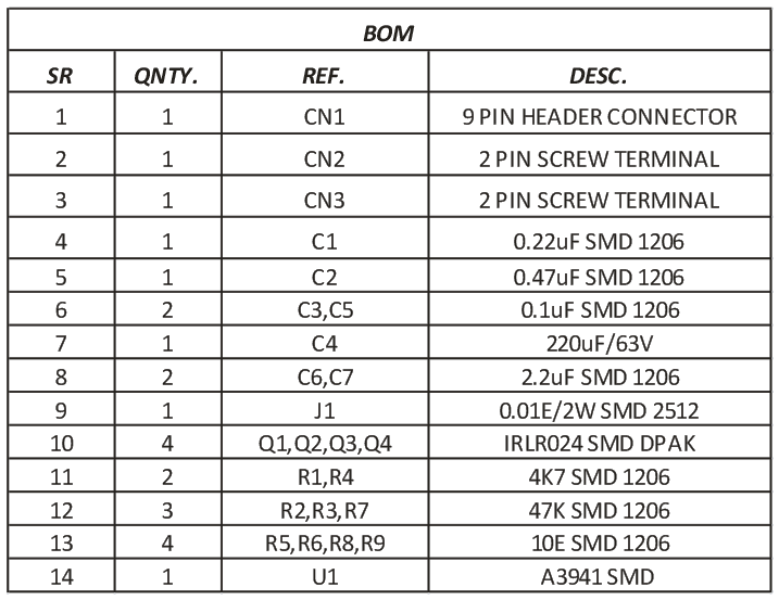
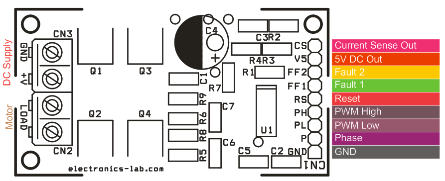
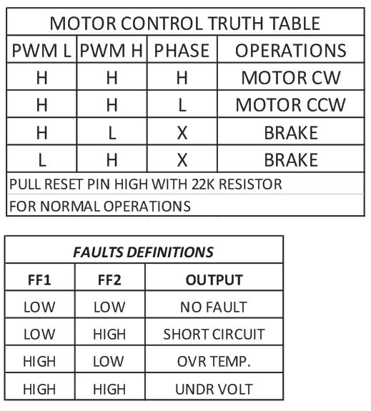
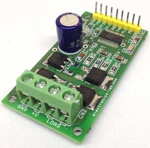
This tiny board is designed to drive a bidirectional DC brushed motor of large current. DC supply is up to 50V DC. A3941 gate driver IC and 4X N Channel Mosfet IRLR024 used as H-Bridge. The project can handle a load of up to 10A. Screw terminals are provided to connect the load and load supply, and 9 Pin header connector is provided for easy interface with the microcontroller. An on board, shunt resistor provides current feedback.
The A3941 is a full-bridge controller for use with external N-channel power MOSFETs and is specifically designed for automotive applications with high-power inductive loads, such as brush DC motors. A unique charge pump regulator provides full (>10 V) gate drive for battery voltages down to 7 V and allows the A3941 to operate with a reduced gate drive, down to 5.5 V. A bootstrap capacitor is used to provide the above-battery supply voltage required for N-channel MOSFETs. An internal charge pump for the high-side drive allows DC (100% duty cycle) operation.
The full bridge can be driven in fast or slow decay modes using diode or synchronous rectification. In the slow decay mode, current recirculation can be through the high-side or the low side FETs. The power FETs are protected from shoot-through by resistor R7 adjustable dead time. Integrated diagnostics provide an indication of under voltage, over temperature, and power bridge faults, and can be configured to protect the power MOSFETs under most short circuit conditions.
The A3941 is a full-bridge MOSFET driver (pre-driver) requiring a single unregulated supply of 7 to 50 V. It includes an integrated 5 V logic supply regulator. The four high current gate drives are capable of driving a wide range of N-channel power MOSFETs, and are configured as two high-side drives and two low-side drives. The A3941 provides all the necessary circuits to ensure that the gate-source voltage of both high-side and low-side external FETs are above 10 V, at supply voltages down to 7 V. For extreme battery voltage drop conditions, correct functional operation is guaranteed at supply voltages down to 5.5 V, but with a reduced gate drive voltage. The A3941 can be driven with a single PWM input from a Microcontroller and can be configured for fast or slow decay. Fast decay can provide four-quadrant motor control, while slow decay is suitable for two-quadrant motor control or simple inductive loads. In slow decay, current recirculation can be through the high-side or the low-side MOSFETs. In either case, bridge efficiency can be enhanced by synchronous rectification. Cross conduction (shoot through) in the external bridge is avoided by an adjustable dead time. A low-power sleep mode allows the A3941, the power bridge, and the load to remain connected to a vehicle battery supply without the need for an additional supply switch. The A3941 includes a number of protection features against under voltage, over temperature, and Power Bridge faults. Fault states enable responses by the device or by the external controller, depending on the fault condition and logic settings. Two fault flag outputs, FF1 and FF2, are provided to signal detected faults to an external controller.
Features
High current gate drive for N-channel MOSFET full bridge
High-side or low-side PWM switching
Charge pump for low supply voltage operation
Top-off charge pump for 100% PWM
Cross-conduction protection with adjustable dead time
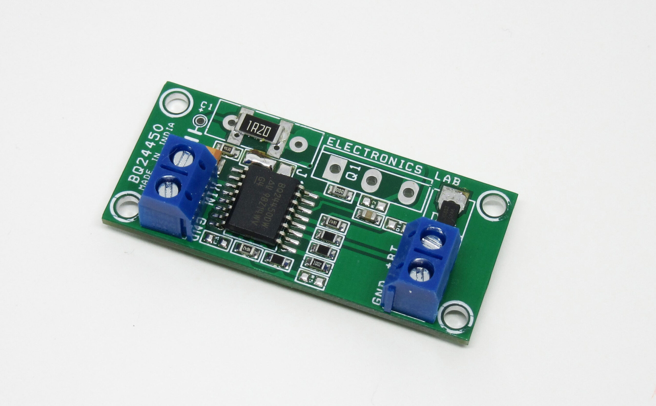
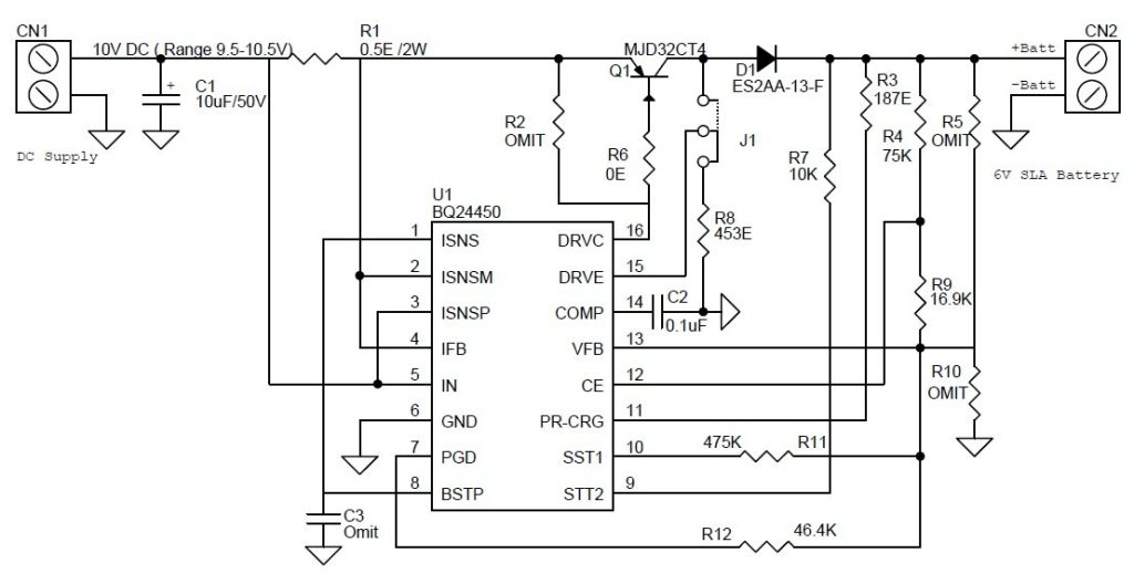
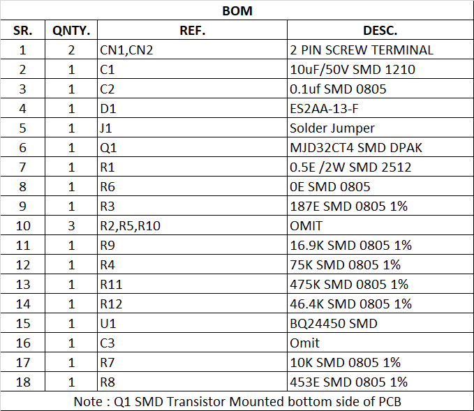
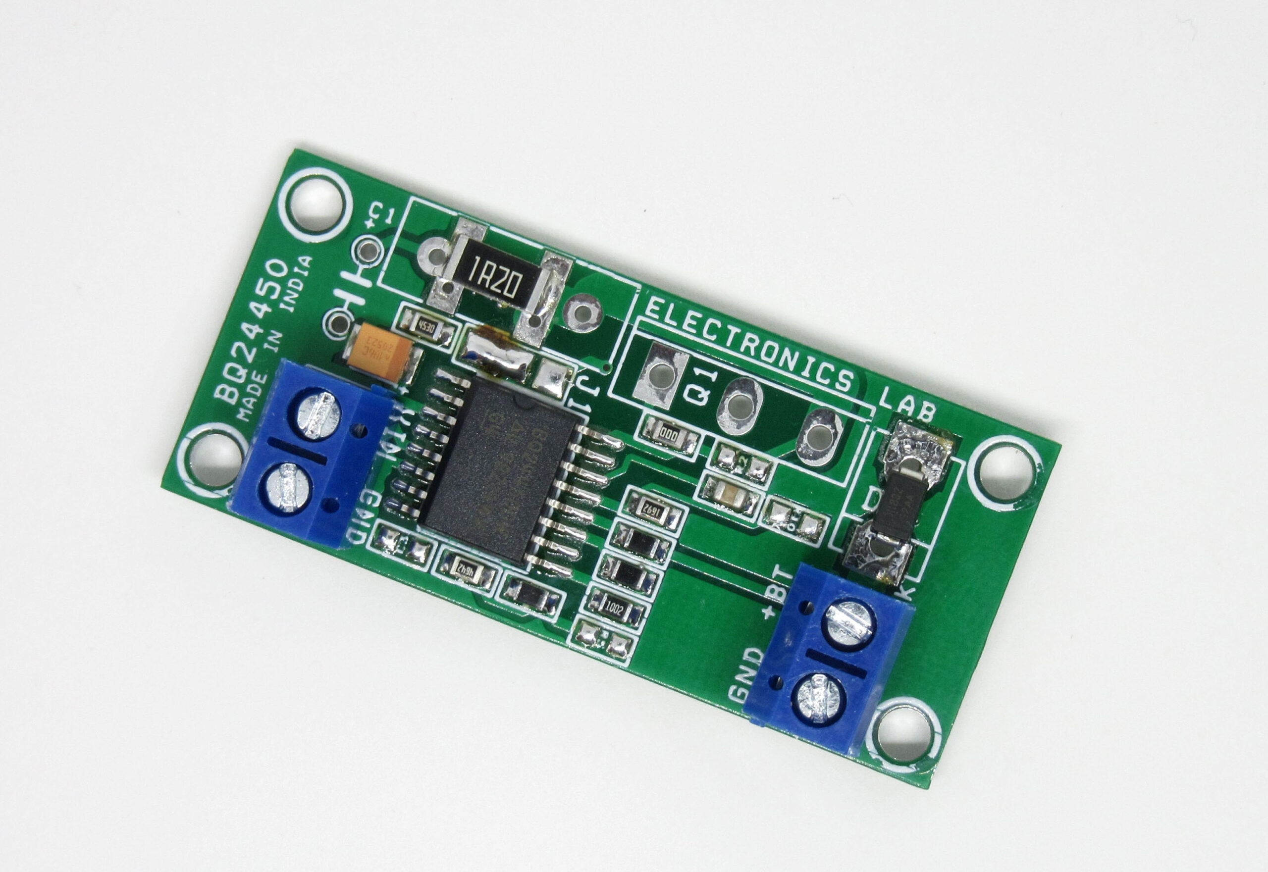
6V Lead acid (SLA) battery charger project is based on BQ24450 IC from Texas instruments. This charger takes all the guesswork out of charging and maintaining your battery, no matter what season it is. Whether you have a Bike, Robot, RC Car, Truck, Boat, RV, Emergency Light, or any other vehicle with a 6v battery, simply hook this charger maintainer up to the battery. The BQ24450 contains all the necessary circuitry to optimally control the charging of lead-acid batteries. The IC controls the charging current as well as the charging voltage to safely and efficiently charge the battery, maximizing battery capacity and life. The IC is configured as a simple constant-voltage float charge controller. The built-in precision voltage reference is especially temperature-compensated to track the characteristics of lead-acid cells, and maintains optimum charging voltage over an extended temperature range without using any external components. The low current consumption of the IC allows for accurate temperature monitoring by minimizing self-heating effects. In addition to the voltage- and current-regulating amplifiers, the IC features comparators that monitor the charging voltage and current. These comparators feed into an internal state machine that sequences the charge cycle.
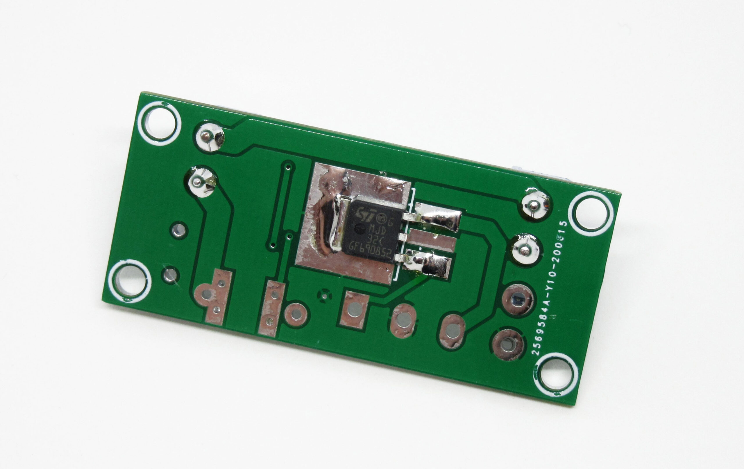
For low charging current, you can use SMD Q1 transistor on the bottom of PCB, for higher charging currents you should use a through-hole (TO247) transistor, like TIP147 on the top of PCB.
The circuit has been designed for PNP transistor (Q1) that’s why the PCB jumper is shorted to R8 by default. You can also use an NPN transistor, in this case, Omit R6, Use R2, Jumper has to be shorted the other way.
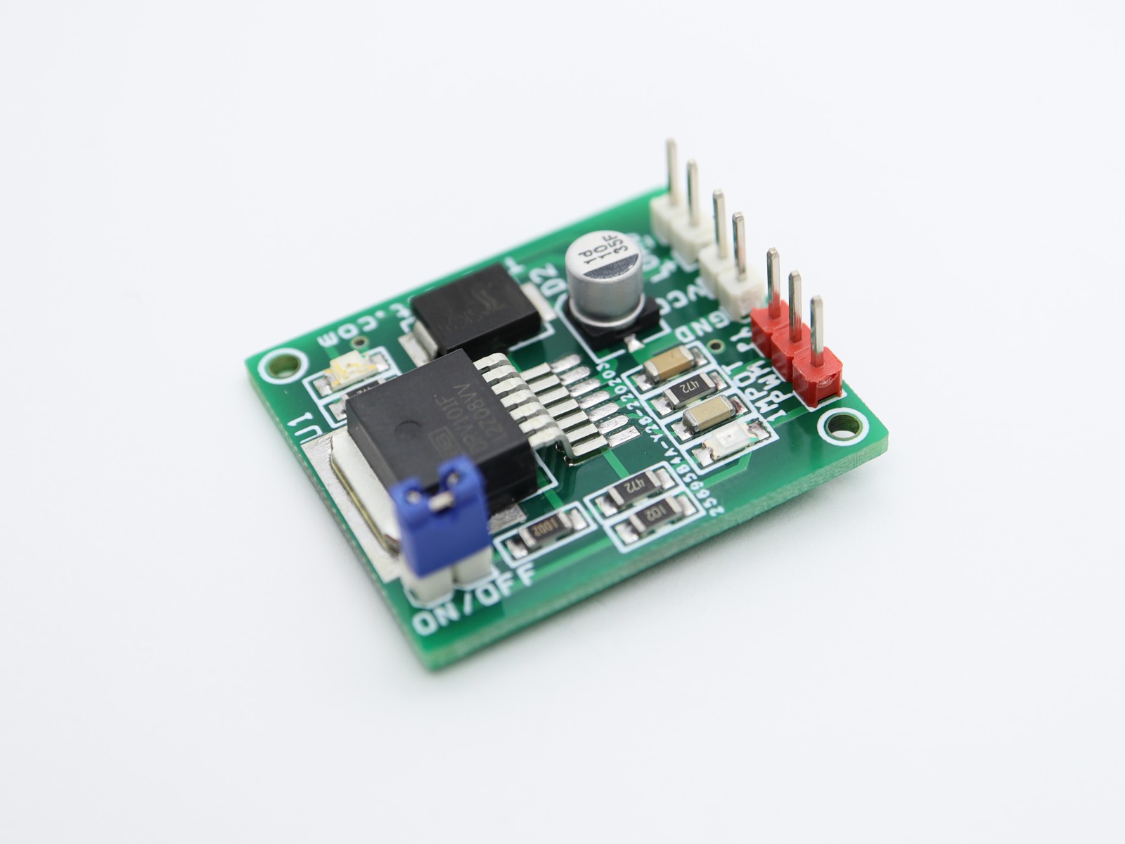
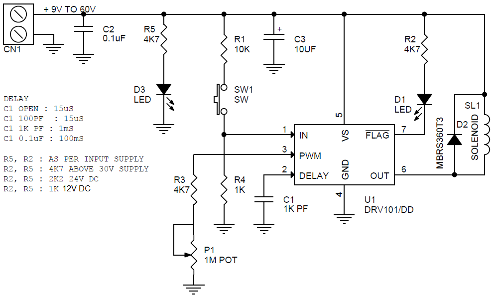
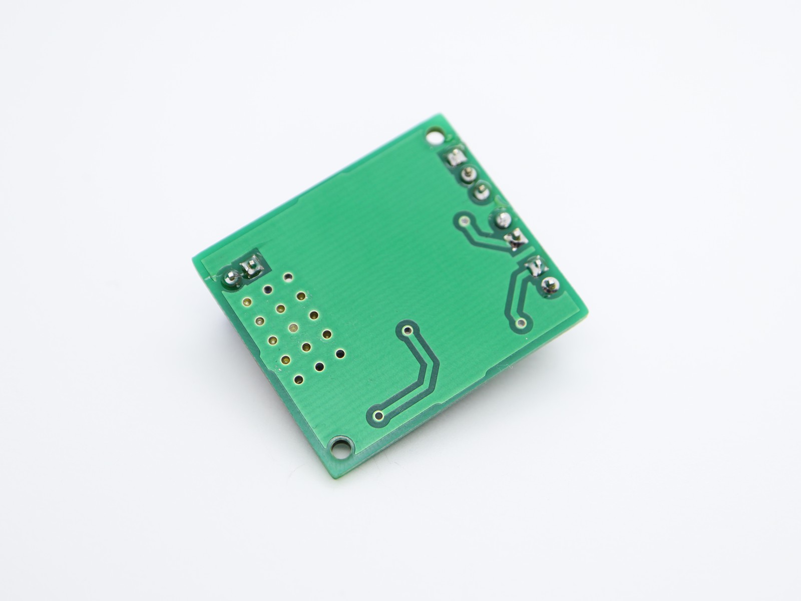
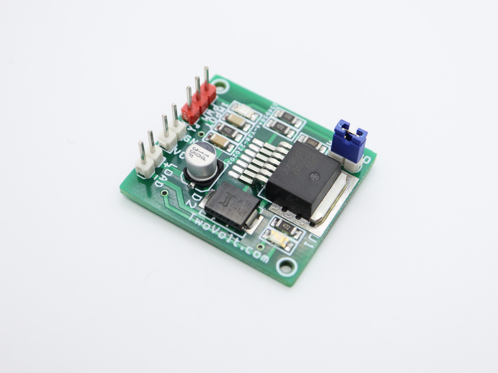
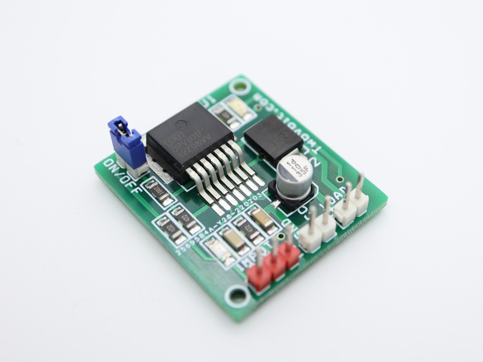
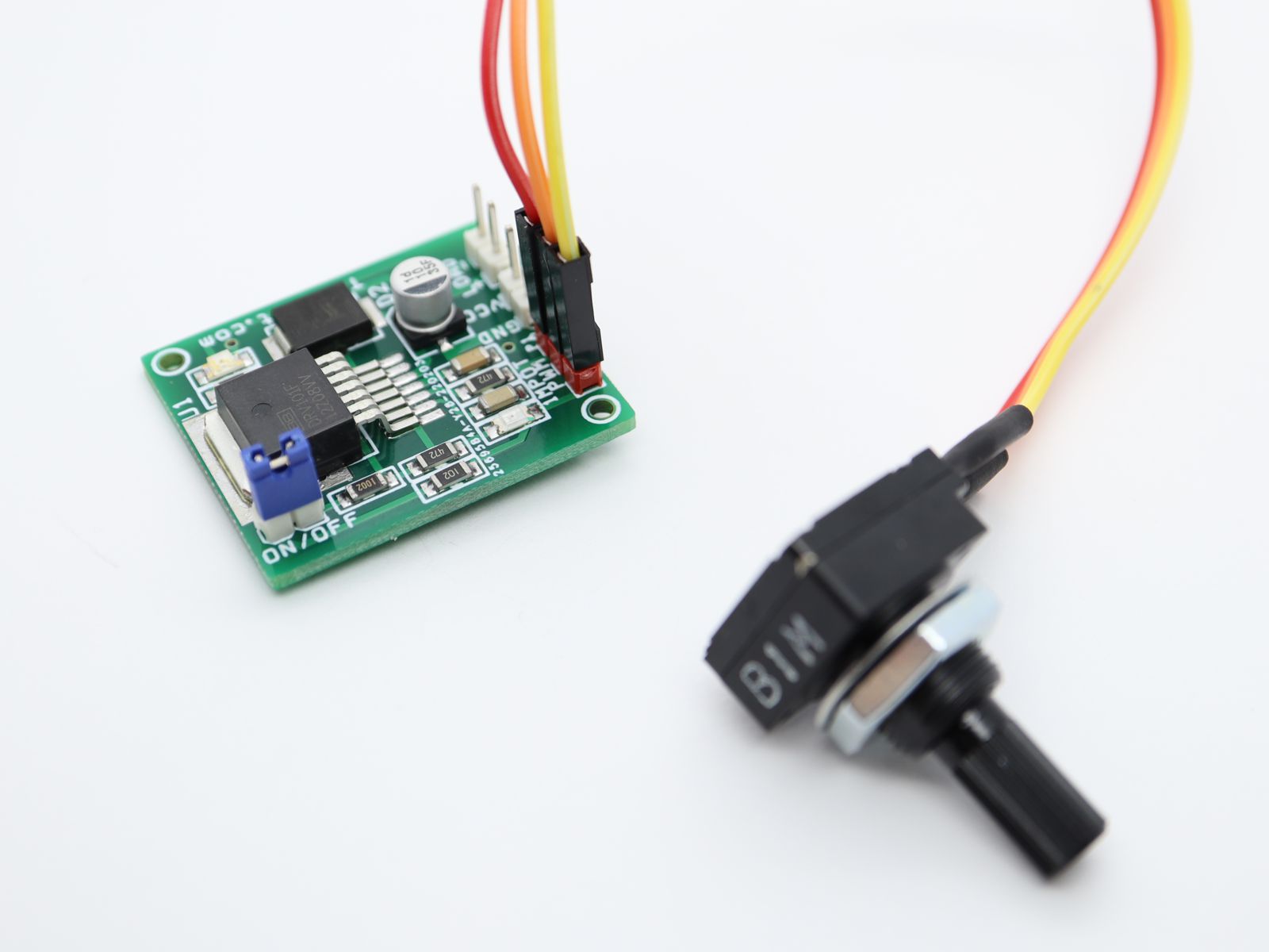
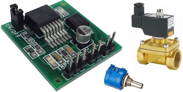
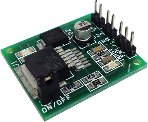
The DRV101 is a low-side power switch employing a pulse-width modulated (PWM) output. Its rugged design is optimized for driving electromechanical devices such as valves, solenoids, relays, actuators, and positioners. The DRV101 module is also ideal for driving thermal devices such as heaters and lamps. PWM operation conserves power and reduces heat rise, resulting in higher reliability. In addition, an adjustable PWM potentiometer allows fine control of the power delivered to the load. Time from dc output to PWM output is externally adjustable. The DRV101 can be set to provide a strong initial closure, automatically switching to a soft hold mode for power savings. The duty cycle can be controlled by a potentiometer, analog voltage, or digital-to-analog converter for versatility. A flag output LED D2 indicates thermal shutdown and over/under current limit. A wide supply range allows use with a variety of actuators.
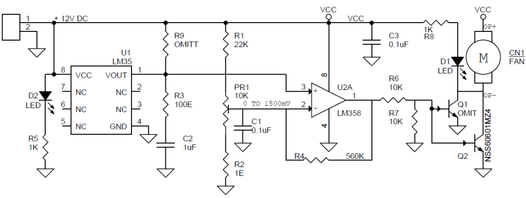
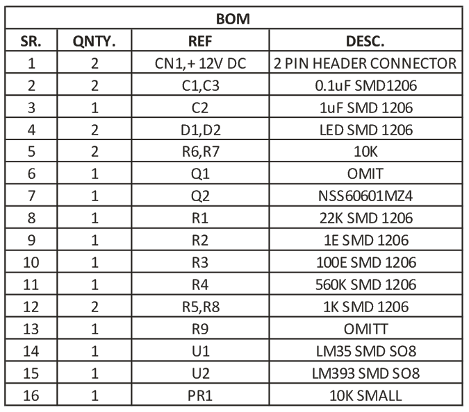
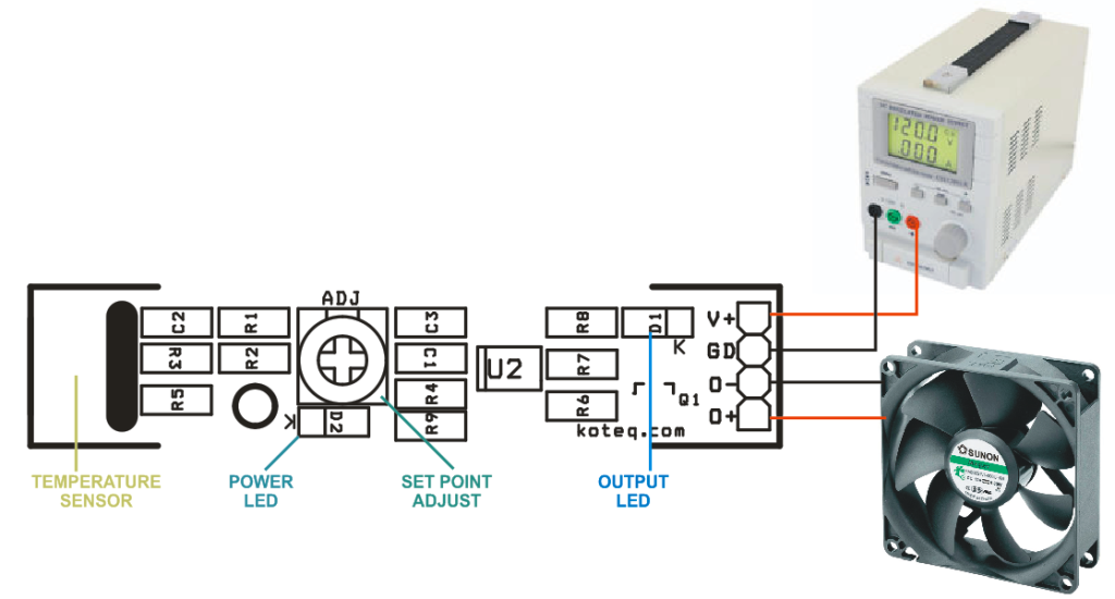
Heat activated cooling fan controller is a simple project which operates a brushless fan when the temperature in a particular area goes above a set point, when temperature return normal, fan automatically turns off. The project is built using LM358 Op-amp and LM35 temperature Sensor. Project requires 12V DC supply and can drive 12V Fan. This project is useful in application like Heat sink temperature controller, PC, heat sensitive equipment, Power supply, Audio Amplifiers, Battery chargers, Oven etc
The SMD SO8 LM35 used as temperature sensor, LM358 act as comparator and provides high output when temperature rise above set point, high output drive the Fan through driver transistor. The LM35 series are precision integrated-circuit temperature devices with an output voltage linearly-proportional to the Centigrade temperature. The LM35 device has an advantage over linear temperature sensors calibrated in Kelvin, as the user is not required to subtract a large constant voltage from the output to obtain convenient Centigrade scaling. The LM35 device does not require any external calibration or trimming to provide typical accuracy of ±¼°C at room temperature. Temperature sensing range 2 to 150 centigrade. LM35 provides output of 10mV/Centigrade.
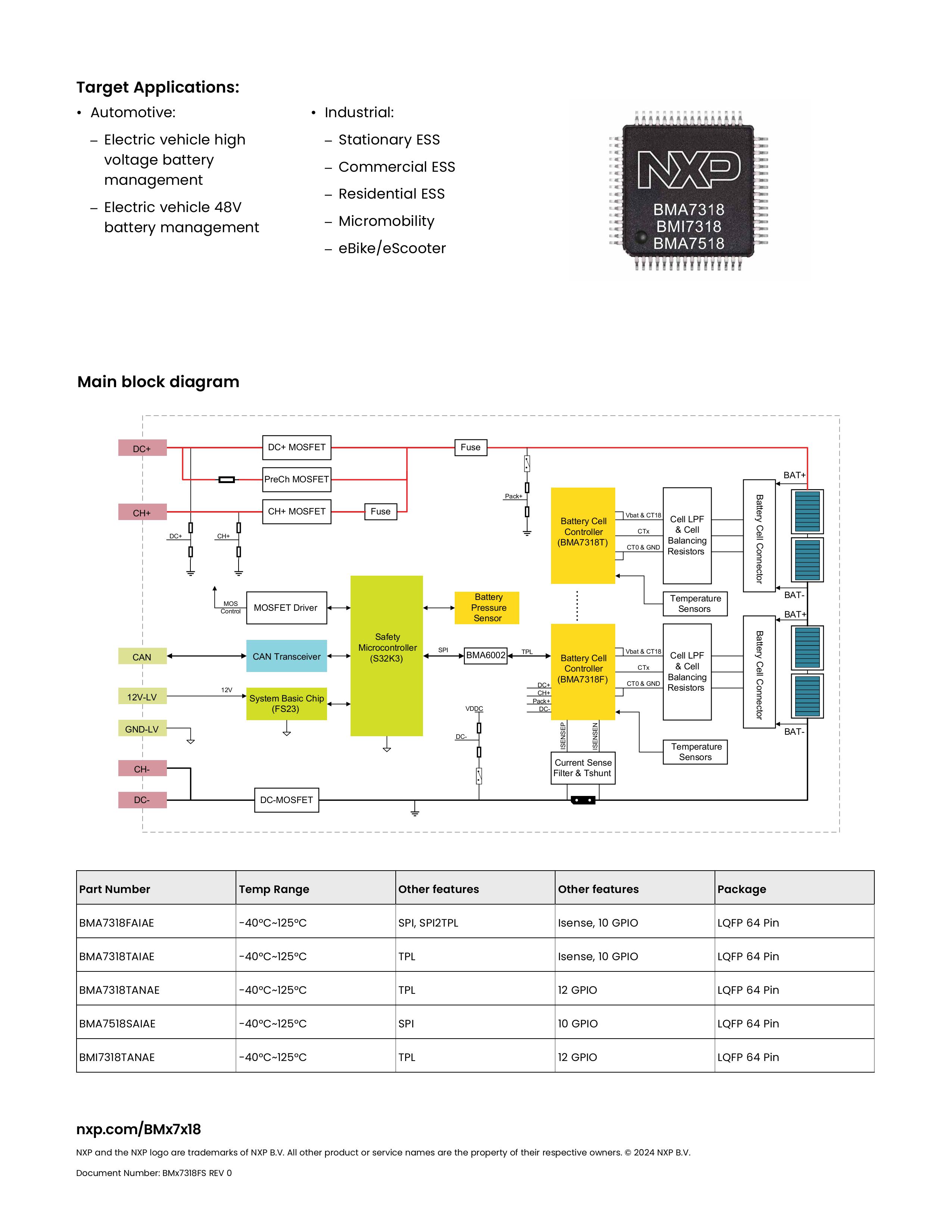
NXP launched BMx7318, a lithium-ion battery cell controller IC. It is an analog front-end product made to monitor battery cells in electric cars and energy storage systems (ESS). It can measure the voltage of 18 battery cells, track the flow of electricity, and monitor up to 12 other important voltages, making it a good solution for managing batteries. The BMx7318 also supports ISO 26262 ASIL C function safety target for automotive applications and SIL2 safety target for industrial applications.
Features of BMx7318
BMx7318 has various feature for managing batteries. Like, it can track the voltage of an 18-channel cell (18 battery cells) at the same time, measure the flow of electricity, and monitor up to 12-channel analog voltage measurement up to 150 mA supporting up to 125 °C ambient temperature. This helps keep an eye on things like temperature and insulation and pack voltage measurement. The AIN channels support pack voltage measurement, temperature measurement, and insulation measurement. The BMx7318 also has smart ways to average out voltage readings measurements through digital filtering, onboard balancing up to 300mA, ultra-low power mode consuming only 5 mA, a dedicated hardware alarm pin for rapid response to overcurrent events and integrated current measurement.
Target Applications
Automotive
Electric vehicle high voltage battery management
Electric vehicle 48V battery management Main block diagram
Industrial
Stationary ESS
Commercial ESS
Residential ESS
Micromobility
eBike/eScooter
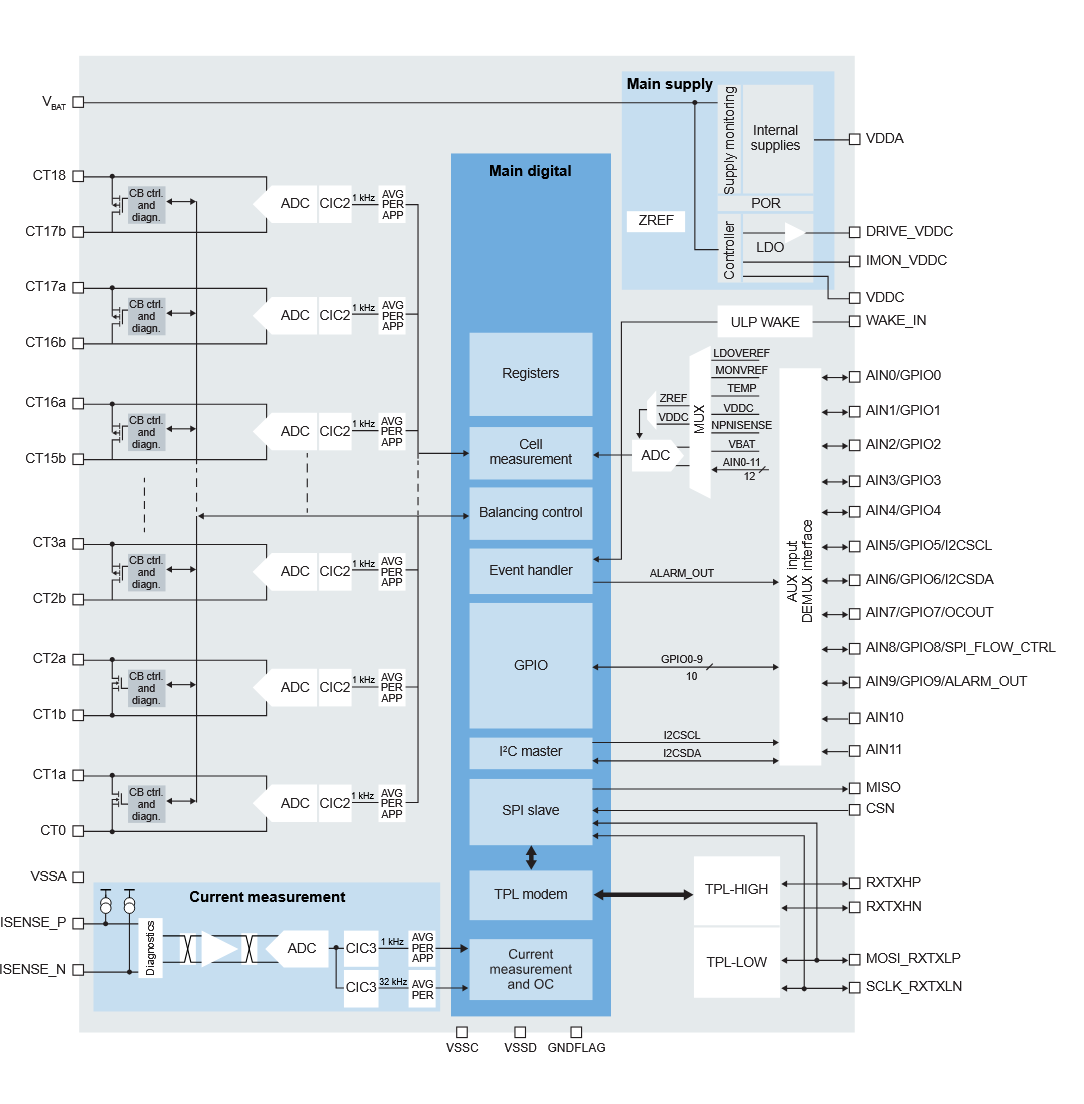
Block Diagram
BMx7318 battery cell controller’s Architecture
The BMx7318 stands out because it can measure battery cell voltage very accurately, with a tiny margin of error of 0.8mV, which means it gives reliable readings that don’t change much over time. It’s also great at measuring voltage in certain systems, with an accuracy of 1mV for LPF voltage platforms, which is critical for applications where voltage stability is essential. Plus, the integrated circuit family design reduces the need for external components by 50% that helps save money.
The BMx7318 is a game-changer for battery management, offering high accuracy and reliability. It has a special feature, its integrated communication bridge (SPI2TPL) that lets devices talk to each other smoothly with isolated 2.0 Mbit/s. Also the product is built to last, supporting up to 25 years of use in ESS applications with an extended mission profile (EMP). Plus, it’s designed to work with other similar devices like BMI7318 through PIN2PIN, giving the system flexibility and room to grow.
Applications
The BMx7318 works with many different types of systems, like electric carsenergy storage and 48V applications. Additionally it has software features that help devices talk to each other, like SPI communication with SPI2TPL bridge function and I2C controller for external devices . These features help designers create good battery management systems that meet modern needs.
Pricing for BMx7318 is not available at the moment. Products are not yet available on the online marketplaces. For more information, you can visit the product page, or check out the Datasheet for the same.
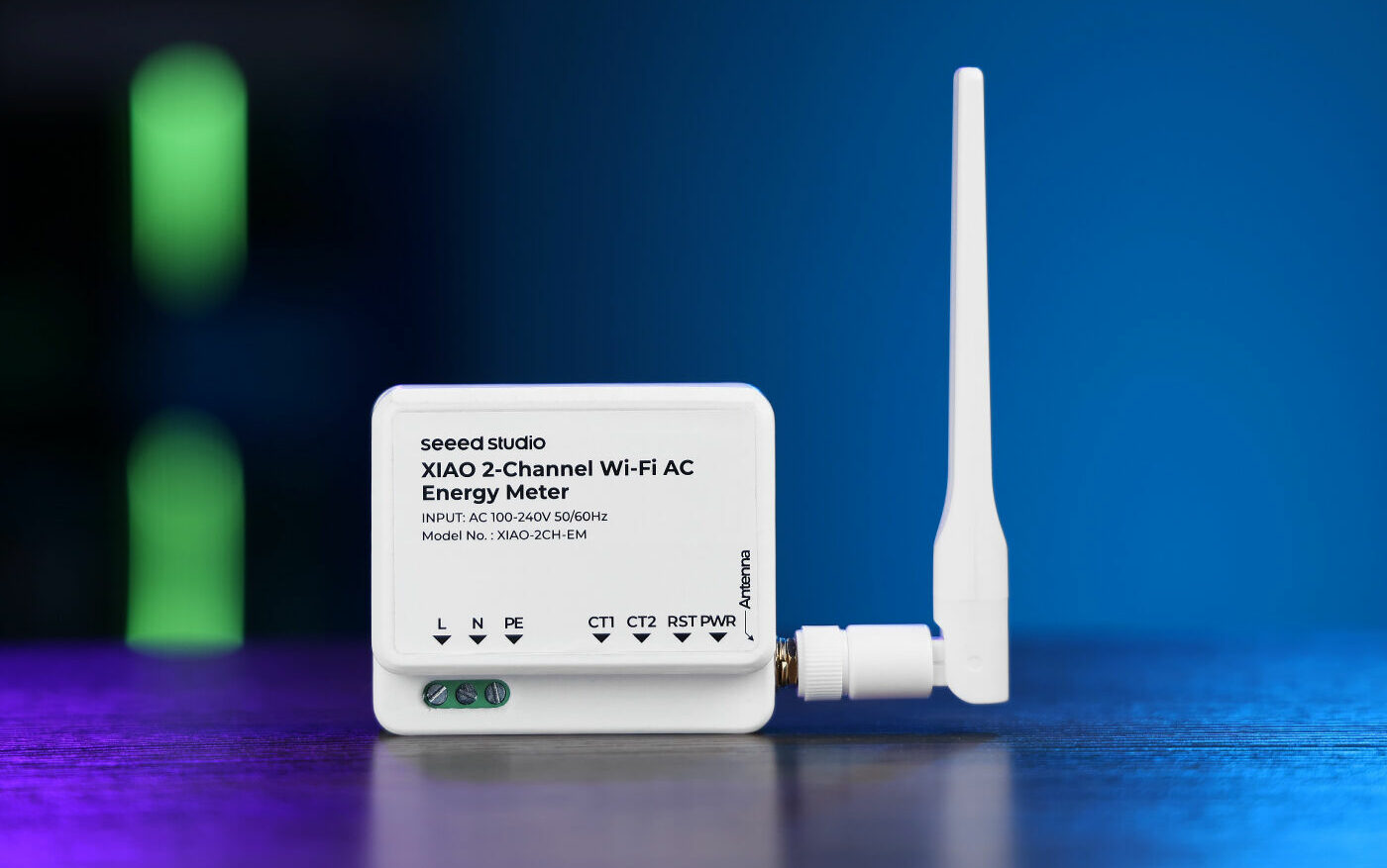
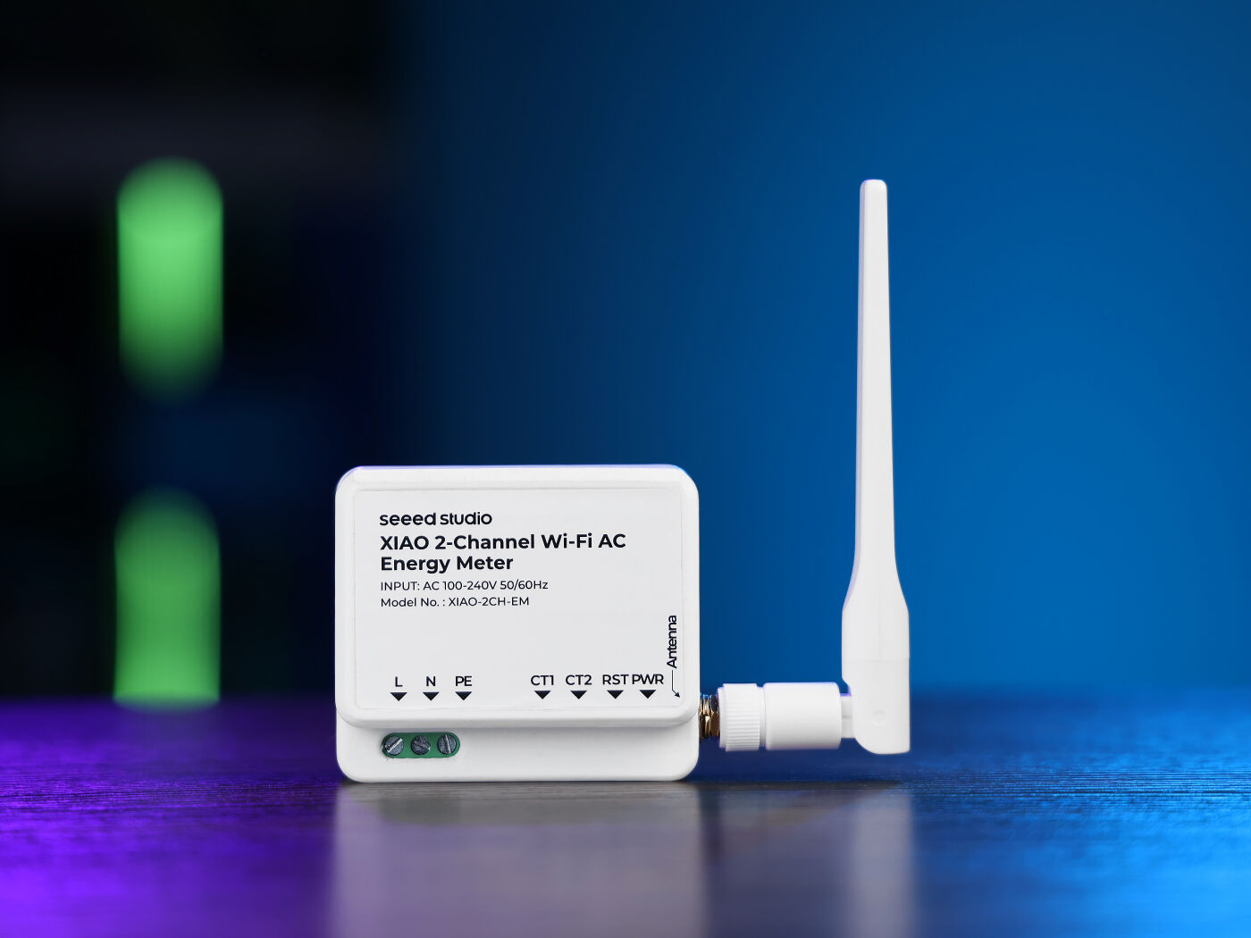
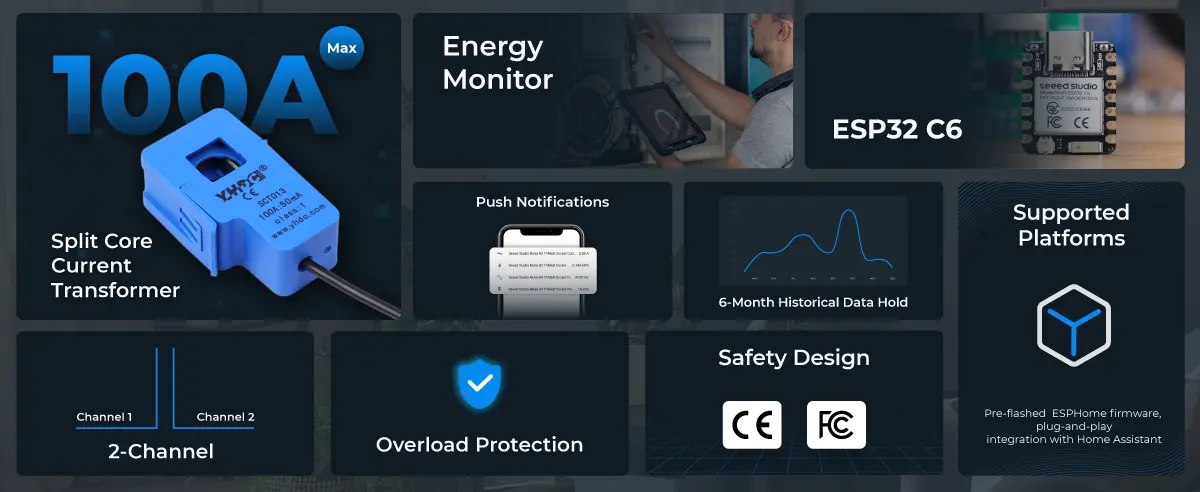
Seeed Studio has recently released XIAO 2-channel Wi-Fi AC Energy Meter, a compact dual-channel power monitoring device based on the ESP32-C6 RISC-V microcontroller. It supports Wi-Fi 6 and is pre-flashed with ESPHome for Home Assistant integration, making it ideal for residential and small-scale energy monitoring, such as solar power tracking and appliance-level energy usage.
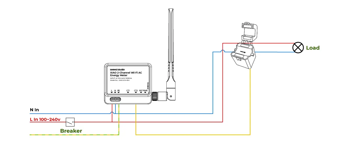
The device features two 100A CT clamps for non-intrusive current sensing, a BL0939 energy metering chip, and supports input voltages from 100-240V AC. The ESP32-C6 offers a 160 MHz core, 512KB SRAM, and 4MB flash. It includes a USB-C port for programming, an external 2.4GHz antenna, and supports Matter, Zigbee, and Thread (though not listed in the product specs). The compact 70 x 58 x 38 mm enclosure is 3D-printed. While the CT clamps support up to 100A, the BL0939 IC limits direct measurement to 35A, though this does not apply in CT mode.
XIAO 2-channel Wi-Fi AC Energy Meter Specifications
(Bluetooth LE, Zigbee 3.0, Thread supported by ESP32-C6, not listed in specs)
Antenna – External 2.4GHz rod antenna (81dBi gain)
USB – 1x USB Type-C port for programming
Power Input Terminals – L (Live), N (Neutral), PE (Protective Earth)
AC Input Rating – 100–240V AC, 50/60Hz
Metering IC – BL0939
Supports direct AC input and CT clamp-based measurements
Current Transformers (CT Clamps)
2x clamp inputs
Detection range: 0–100A per clamp
Accuracy: ±1%
Turns ratio: 1:2000
Dielectric strength: AC 3.5KV/1min
Measurement Range (direct measurement)
Current: 10mA–35A @ 1mΩ
Power: 1W to 7700W
Firmware – Pre-flashed with ESPHome for Home Assistant
Enclosure – 3D-printed case
Dimensions – 70 x 58 x 38 mm
Feature overview
The XIAO 2-channel Wi-Fi AC Energy Meter comes pre-flashed with ESPHome firmware, for native integration with Home Assistant for real-time energy monitoring across two AC circuits. It supports OTA (Over-the-Air) updates and YAML-based configuration, allowing users to define sensors, calibration values, and reporting intervals. The ESP32-C6 also supports Matter, Zigbee 3.0, Thread, and Bluetooth LE/Mesh, although these protocols are not enabled by default in the provided firmware. So if you want to enable those features, you have to write your own script using the Arduino IDE, PlatformIO, or ESP-IDF for full control.
Seeed Studio provides wiring instructions for the CT clamps and guides to set up the XIAO 2-channel Wi-Fi AC Energy Meter with the Home Assistant Green gateway. A power consumption chart is available directly in the Home Assistant dashboard once configured.
The XIAO energy meter costs $29.32 on AliExpress and $28.70 on Seeed’s store, with Amazon availability coming soon.
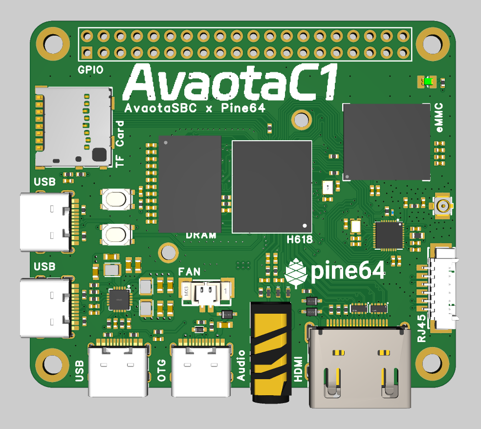
Avaota C1 Development Board is the upcoming single-board computer (SBC) in the AvaotaSBC family having Raspberry Pi A form factor designed for flexible and scalable DIY electronics and embedded system projects. Powered by an ARM-based Allwinner H618 SoC, C1 Development Board is a variant of the Yuzuki Chameleon. It provides extensive connectivity for various sensors and actuators whilst supporting high-resolution video output at fairly high refresh rate, making it ideal for embedded development, image and audio processing, smart devices, IoT applications, and prototyping.
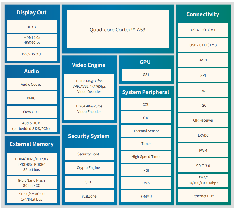
The Avaota C1 features a quad-core ARM Cortex-A53 CPU with 64-bit architecture and a multi-core Mali G31 GPU. The SBC can output 4K video at 60 fps via its HDMI interface and also supports SPI display connections. The board also supports low-latency 4K H.264 encoding at 25 frames per second and is compatible with HDR10 and HLG. Image quality is enhanced with Allwinner’s SmartColor 3.3 picture engine. Wireless connectivity is provided by the onboard AIC8800DC W-Fi cum Bluetooth chip. Based on the watermark on the SBC, C1 device appears to be a collaboration between Avaota and Pine64.
Avaota C1 Development Board Specifications:
SoC:Allwinner H618 quad-core Arm Cortex-A53 processor @ up to 1.5GHz with 1MB L2 cache and Arm Mali-G31 MP2 GPU
System Memory: 1GB DRAM
Storage: up to 128 GB onboard eMMC flash, MicroSD card socket
Display Interface: Optional 3.5-inch (320×480) or 1.54-inch (240×240) SPI displays
Video Output:
HDMI 2.0a up to 4Kp60
TV Video composite (CVBS)
VPU:
VP9-10 Profile-2 up to 6Kp30
H.265 HEVC MP-10 @ L5.1 up to 6Kp30
AVS2 up to 4Kp60
H.264 AVC HP @ L5.1 up to 4Kp25
H.264 MVC up to 1080p60
Audio:
Digital audio output via HDMI
Digital PDM Microphone (DMIC)
Audio HUB (Embedded 3 I2S/PCM)
Wireless Connectivity:
Lead out RJ45 1000M interface via Ethernet PHY
Onboard AIC8800DC W-Fi cum Bluetooth chip
USB: 4x USB Type C, 3x USB2.0 HOST and 1x USB2.0 OTG, support USB camera and capture card input
In recent times, Boardcon unveiled the 6TOPS AI-capable LGA3576, a state-of-the-art embedded system-on-module (SoM) with a 330-pad LGA layout that is powered by the Rockchip RK3576 AI SoC and the Idea3576 single board computer (SBC). It safeguards seamless multitasking for applications including 4K/8K video surveillance, digital signage, AV processing systems and AIoT edge devices (smart retail, robotics) with an intelligent hybrid CPU architecture (4x Cortex-A72 @ 2.2GHz + 4x Cortex-A53 @ 1.8GHz).
All I/Os, encompassing HDMI, PCIe, Ethernet, and GPIO signals, find themselves subjected through LGA pads, and the LGA3576 SoM accommodates up to 8GB LPDDR5 and 512GB UFS storage. Power management is administered by an RK806S-5 PMIC. Cameras, displays, network modules, and peripherals are capable of being expanded in a variety of ways with the LGA3576’s extensive I/O suite, which includes UART, USB 3.2 Type-C, HDMI/DP, and MIPI CSI/DSI. It streamlines networking and storage with its dual SDMMC and GMAC interfaces.
Previously, we have covered many SoM and development boards powered by the Rockchip RK3576 SoC, including the Mekotronics R57, the ASUS Chromebox 5a, the Banana Pi BPI-M5 Pro, and much more. Feel free to check those out if you’re interested in the topic.
Broadcon LGA3576 Specifications:
CPU: Octa-core processor with 4x Cortex-A72 @ 2.2GHz, 4x Cortex-A53 @ 1.8GHz, and 1x Cortex-M0 real-time core
GPU: Arm Mali-G52 MC3 GPU with OpenGL ES 1.1/2.0/3.2, OpenCL 2.0, and Vulkan 1.1 support
NPU: 6 TOPS AI accelerator supporting INT4/INT8/INT16/BF16/TF32 operations
VPU:
Decoding:
H.265, VP9, AV1, AVS2 up to 8K@30fps or 4K@120fps
H.264/AVC up to 4K@60fps
MJPEG up to 4K@60fps
Encoding: H.264, H.265, (M)JPEG up to 4K@60fps
Memory: 4GB or 8GB LPDDR5 RAM
Storage:
Onboard UFS options: 32GB, 64GB, 128GB, 256GB, or 512GB
2x SDMMC interfaces
Display: HDMI/DP, RGB/EBC, MIPI DSI
Camera: 3x 4-lane MIPI CSI interfaces
Audio: SAI and S/PDIF Rx
Networking: Dual RGMII Ethernet or 1x GMAC + 1x SAI
USB: USB 3.2 Type-C
PCIe: 2x PCIe interfaces
Analog I/O: 7x SARADC
Low-speed I/O: 4x UART, 5x I2C, PWM, GPIO
Power Supply: 3.4V to 5.5V DC input
Form Factor:
330-pin LGA package (10-layer PCB)
Dimensions: 45 x 30mm; ball sizes: 0.4mm/0.35mm; pitch: 1.25mm
Temperature Range:
Operating: 0°C to 70°C
Storage: -40°C to +85°C
Coming to the software section, Boardcon provides support for Debian 12 Buildroot (Linux 6.1.99) and Ubuntu 22.04 as a cross-compiler environment. SW Debugging tools include SecureCRT, AndroidTool.exe, and ADB.
Although the pricing information have not been publicly revealed by Broadcon Embedded Design, but users will still find a hardware manual and other information on the product page.
TexHoo has recently introduced the 12th Generation low-power pocket-sized office mini PC named as QN15. Powered by the Quad-core Intel Twin Lake N150 processor, the TexHoo QN15 mini PC in its barebone configuration supports Wi-Fi 5, with no RAM and storage support.
Without any barebone configuration, the TexHoo QN15 mini PC supports DDR4 SO-DIMM memory as well as NVMe and SATA storage, and offers two 4K-capable HDMI ports, Gigabit Ethernet, a M.2 2230 socket for Wi-Fi 5 and Bluetooth 4.0, and five USB ports with two USB 3.2, two USB 2.0, and a USB Type-C port.
Processor: Intel 12th Gen N150 “Twin Lake” quad-core SoC @ up to 3.6GHz (Turbo), 4 threads, 6MB Smart Cache, Intel UHD Graphics (24EU @ 1.0GHz), 6W TDP
Memory: Single SO-DIMM slot supporting up to 16GB DDR4-2666/3200MHz RAM
Storage:
M.2 2280 socket for SATA III or NVMe SSD
2.5-inch SATA drive bay (proprietary SATA cable required)
Video outputs: 2x HDMI 2.0 ports supporting 4K@60Hz, VP9, and H.265/HEVC decoding
Audio:
3.5mm headphone/mic combo jack
Digital audio output via HDMI
Networking:
Gigabit Ethernet (Realtek LAN)
Optional Wi-Fi 5/6 via M.2 2230 slot
USB:
2x USB 3.2 ports
2x USB 2.0 ports
1x USB Type-C (data only, no display)
Misc:
Power button, CMOS reset pinhole
Cooling fan with dedicated thermal board
Power: 12V/3A via DC jack
Dimensions: 116.3 x 116 x 46 mm
Difference between QN10, QN11 and QN15
Coming to the software part, the barebone version of TexHoo QN15 mini PC ships without an operating system, but variants with 8GB or 16GB RAM, and a 128GB, 256GB, or 512GB SSD ship with Windows 11.
The AliExpress store has three barebone models of TexHoo QN15 mini PC supporting Wi-Fi 5: the QN15 for $98.07, the QN11 for $95.13. and the QN10 for $107.88.
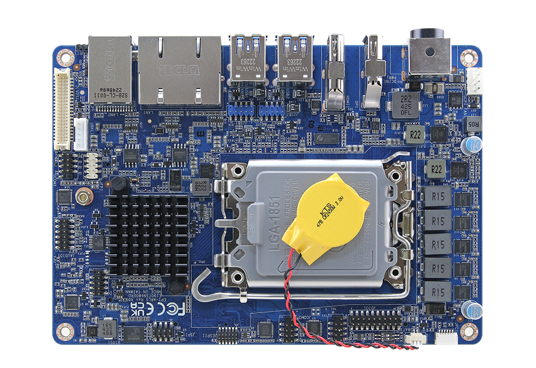
Avalue Technology has introduced the EPI-ARLS, an EPIC SBC that is Explicitly Parallel Instruction Computing single-board computer, specifically designed for industrial and embedded applications. It meets the requirements of smart manufacturing, healthcare monitoring, edge computing, and precision in agriculture. With its small size, fast processing, rich I/O connectivity, and versatile expansion, the EPI-ARLS is good for small space-constrained environments that need quick data processing.
1 x 262pin SO-DIMM Up to 48GB Dual Channel DDR5 5600/6400MHz
1 x M.2 Key M 2280, support PCI-e x4 Gen4 NVMe or SATA device
1 x M.2 Key M 2242, support PCI-e x4 Gen4 NVMe or SATA device (for Q870 only)
Graphics
Intel Xe LPG graphics architecture CPU integrated
Connectivity:
Dual 2.5G Gigabit ethernet
I/O ports:
USB-4 x USB 3.2 Gen 2 at I/O for Q870
4 x USB 2.0 ports by pin header
COM Port-2 x RS-232/RS422/485, 2 x RS-232
GPIO-1 x 16-bit GPIO
OS
Windows 11, Linux
Expansions:
1 x M.2 Key E 2230
1 x M.2 Key M 2280
1 x M.2 Key M 2242
Power Requirement
DC in +12V
Dimensions:
165 x 115 mm
Operating Temp.
0~60°C w/HDD/SSD, ambient 0.5m/s air flow
Weight
0.70lbs (0.3kg)
Features of the EPIC EPI-ARLS SBC
The EPI-ARLS has versatile features to fulfill the needs of industries. It has Intel Core Ultra processors that provides powerful and effective performance, while its small size 165 x 115 mm EPIC form factor ensures fast data analysis and AI tasks management. The device also offers many I/O options, including multiple LAN ports, USB ports, and COM ports, as well as a 16-bit GPIO and TPM 2.0 for secure industrial connectivity. Additionally, the EPI-ARLS supports tri-display output from DP, HDMI, and LVDS/eDP interfaces for better industrial imaging and visual applications. It has integrated 12th gen Intel Xe LPG graphics architecture CPU integrated which perform well for everyday computing and light gaming.
The EPI-ARLS‘s single DDR5 SO-DIMM slot supports up to 48GB of memory, for fast data processing and AI inference. The SBC has M.2 Key-E and Key-M slots for adding wireless modules, NVMe SSDs, and SATA devices. The EPI-ARLS also features dual 2.5G Gigabit Ethernet ports to ensure fast data transfer. Plus, it can handle super high-resolution displays for up to 8K resolution via DP and HDMI interfaces. Compared to Mini-ITX platforms, the EPI-ARLS is smaller without losing any power or flexibility.
Software Support
The EPI-ARLS has integrated Windows 11, Linux and can run many software programs, for manufacturing, healthcare, and farming. It can be a fit for automating industrial tasks, robotics, and high speed cameras. The device can also connect to multiple displays and show HD quality image.
Pricing for EPI-ARLS is not available at the moment. Products are yet not available on the online marketplaces. For more information, you can visit the press release, the Avalue Website, or contact using their online contact form.
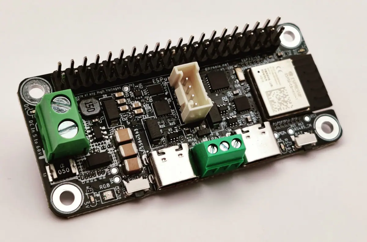
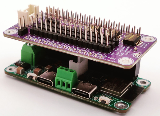
The ESPuno Pi Zero is about the same size as a Raspberry Pi Zero, with the ESP32-C6-MINI-1 wireless module. It has some wireless capabilities, including WiFi 6, Bluetooth 5.0, and 802.15.4 radio for Thread/Zigbee for smart home devices, and comes with various connection options like GPIO, Grove, and RS-485.
The ESPuno Pi Zero is powered by a small computer chip ESP32-C6-MINI-1-N4 or ESP32-C6-MINI-1U-N4 SoC that has a single-core 32-bit RISC-V processor working at speeds of up to 160 MHz. It is a compact board that packs a lot of features into a small space that can connect to wireless networks. It has dual USB-C ports, one for UART and the other for the ESP32-C6, that make it easy to program and test projects. The board’s SMPS enables it to handle a wide range of power inputs, up to 60V DC, which makes it great for industrial and smart device projects. It also has useful features like a real-time clock, a reset button, and a user button provide convenient functionality.
Specifications of ESPuno Pi Zero
Processor:
Single-core 32-bit RISC-V clocked up to 160 MHz
Low-power RISC-V core
System-on-Chip (SoC):
ESP32-C6-MINI-1-N4 or ESP32-C6-MINI-1U-N4
Espressif Systems ESP32-C6 single-core 32-bit RISC-V clocked up to 160 MHz 320KB ROM, 512KB SRAM, low-power RISC-V core up to 20 MHz
Memory/Storage :
320KB ROM, 512KB SRAM
4MB flash
64Kbit 24C64 I2C EEPROM
Wireless Connectivity:
– 2.4 GHz WiFi 6, Bluetooth 5.0, and 802.15.4 radio (for Thread/Zigbee)
USB:
1x USB Type-C UART (CH343P) port
1x USB Type-C port connected to ESP32-C6
Expansions:
40-pin Raspberry Pi-compatible GPIO header via PCA9671 GPIO extender
ESPuno Pi Zero shown with a PGEZ Stackable Port Expander
Software Support of the ESPuno Pi Zero
The ESPuno Pi Zero has a lot of software options, like Arduino, CircuitPython, ESP-IDF framework, PlatformIO, Tasmota, ESPHome and others. This means developers can pick the programming environment and framework style they like best. The board can be used for many things, like STEM education, RS485, DMX/DMX512 lighting systems, Modbus RTU control, solar energy monitoring, robotics, drones, and industrial automation.
For more information, you can visit the product page. The ESPuno Pi Zero is live on Kickstarter, launched by DitroniX, with a £1000 funding target. You can pledge £19 (about $26) for a single board with a PCB antenna or £24 (about $32) with an external antenna.
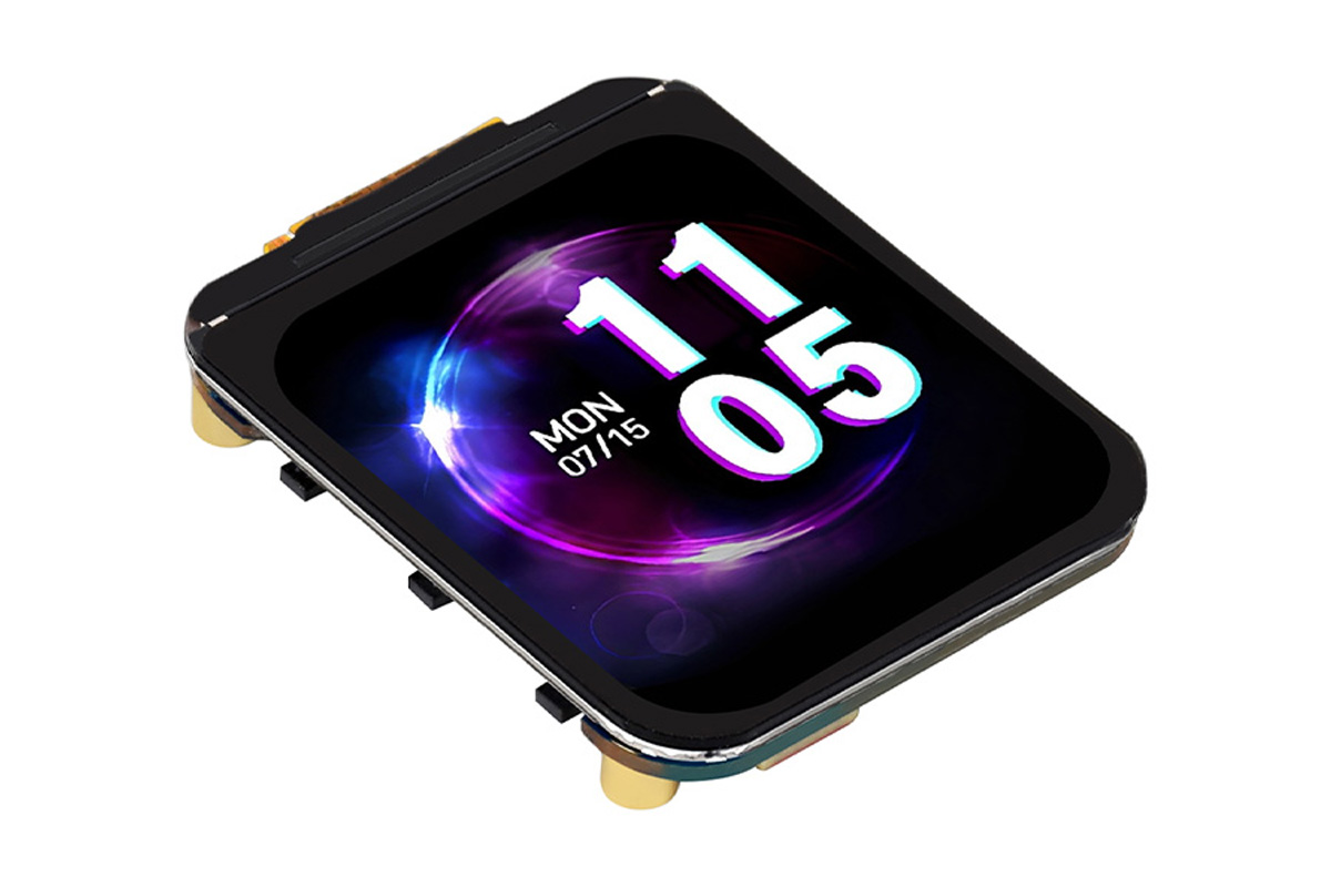
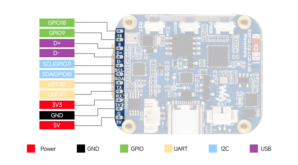
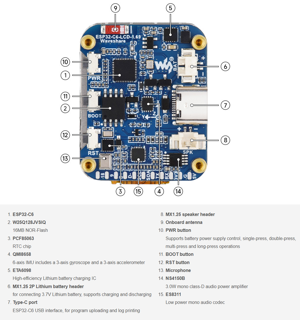
Waveshare has recently launched ESP32-C6-LCD-1.69, a 1.69-inch AI development board with a 240×280 IPS color display, built around the ESP32-C6 SoC with Wi-Fi 6, Bluetooth 5, and IEEE 802.15.4 support. The board is ideal for smart IoT applications, including AI voice interaction, wearable devices, and compact control interfaces.
The board comes with 16MB Flash, a 6-axis IMU (QMI8658), RTC (PCF85063), microphone, speaker, and an ES8311 audio codec. Display control is handled by an ST7789V2 via SPI. The board also includes a USB Type-C port, lithium battery management (charging/discharging), RST/BOOT/user buttons, and reserved pads for GPIO, I2C, USB, and UART expansion. Its AI speech capability enables compatibility with platforms like DeepSeek or Doubao.
ESP32-C6-LCD-1.69 AI development board specifications
SoC: ESP32-C6 with:
32-bit RISC-V core @ up to 160 MHz (main), 20 MHz (low-power)
Wi-Fi 6, Bluetooth 5 (LE), IEEE 802.15.4 (Zigbee/Thread)
Memory: 320 KB ROM, 512 KB HP SRAM, 16 KB LP SRAM, 16MB NOR Flash
Battery: MX1.25 header for 3.7V Li-ion battery, with ETA6098 charger
Connectivity: USB Type-C (program/debug), onboard antenna
Buttons: BOOT, RST, PWR (multi-function), programmable user button
Expansion: Reserved pads for GPIO, I2C, UART, USB
Dimensions: 30 mm x 37.12 mm
The board supports ESP-IDF v5.x+ which includes RISC-V toolchain support and libraries for Wi-Fi 6, BLE Mesh, Zigbee (via OpenThread), and AI voice integration through ESP-ADF. Developers can access ST7789V2 display drivers, ES8311 audio libraries, and sensor APIs for the QMI8658 IMU and PCF85063 RTC via the ESP-IDF libraries or community repositories. More information can be found on the company’s Wiki page.
The ESP32-C6-LCD-1.69 AI development board is available on AliExpress for $17.19, but on the Waveshare store, you can get it for $15.99, but that price does nto include shipping.
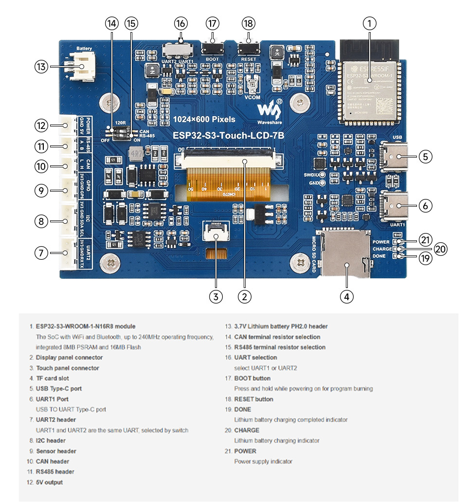
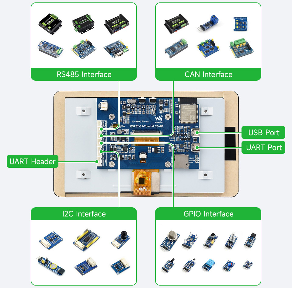
Waveshare has recently launched ESP32-S3-Touch-LCD-7B, an ESP32-S3-based 7-inch Display Development Board with a 1024×600 IPS display and optional capacitive touch support. It’s designed for rapid HMI development with Wi-Fi and Bluetooth connectivity, high-resolution GUI support, and multiple expansion interfaces, making it ideal for smart control panels, industrial displays, or embedded GUI projects.
The display supports 2.4GHz Wi-Fi, Bluetooth 5 (BLE), and includes interfaces like CAN, RS485, I2C, and an SD card slot for storage. The display supports 5-point capacitive touch (on the touch version) via I2C, along with interrupt support. It can run on battery, supports backlight control, onboard antenna, USB Type-C for power and data, and there are dual UART options for communication. The board features LED indicators for power and charge status, as well as support for real-time battery voltage monitoring and low-power modes.
Waveshare ESP32-S3-Touch-LCD-7B Specifications
SoC: Espressif ESP32-S3 dual-core LX7 processor @ up to 240MHz with Wi-Fi 4 & Bluetooth 5 (LE)
Memory: 512KB SRAM + 384KB ROM
Storage:
16MB onboard Flash, 8MB PSRAM
1x SD card slot
Display
7-inch IPS panel, 1024×600 resolution
170° viewing angle
Backlight adjustable
5-point capacitive touch (optional, via I2C)
Wireless: 2.4GHz Wi-Fi (802.11 b/g/n), Bluetooth 5 BLE, onboard antenna
USB:
USB Type-C (USB device/full-speed)
USB-to-UART Type-C port
Expansion:
1x CAN header
1x RS485 header
1x I2C header
1x Sensor header
Dual UART (switchable between UART1 and UART2)
Misc:
BOOT RESET and POWER button
CHARGE, and DONE (charging complete) indicator
Power:
3.7V Li-ion battery support (PH2.0)
Battery charging and monitoring with status LEDs
5V power out
Low-power modes supported
Dimensions:
With touch: 192.96 × 110.76 mm
Without touch: 165.72 × 97.60 mm
ESP32-S3 7-inch Display Development Board Hardware Overview
The board is fully compatible with the ESP-IDF, enabling native support for features like capacitive touch, LVGL GUI rendering, USB device functionality, and multiple serial protocols. It also supports Arduino and MicroPython environments. Waveshare also provides example code and documentation on their Wiki, including demo projects for display control, touch input, and CAN/RS485 communication.
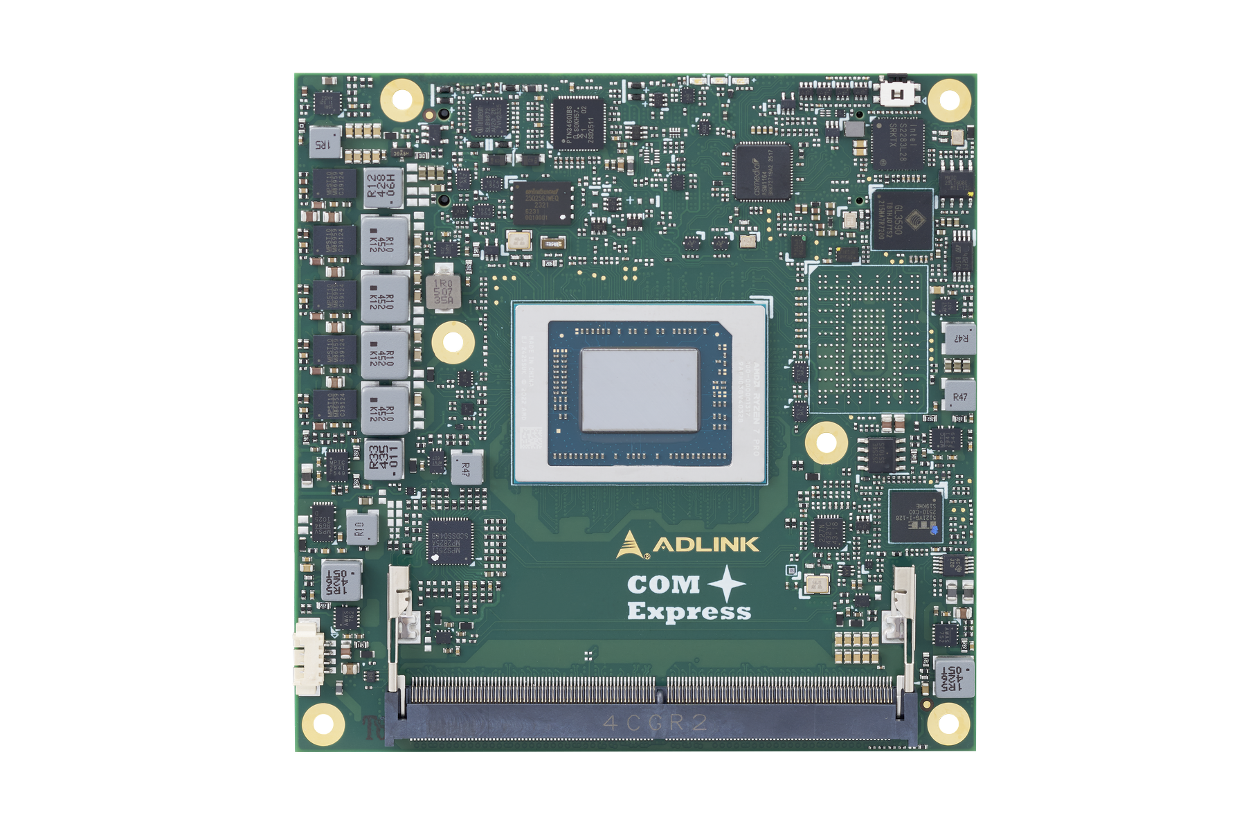
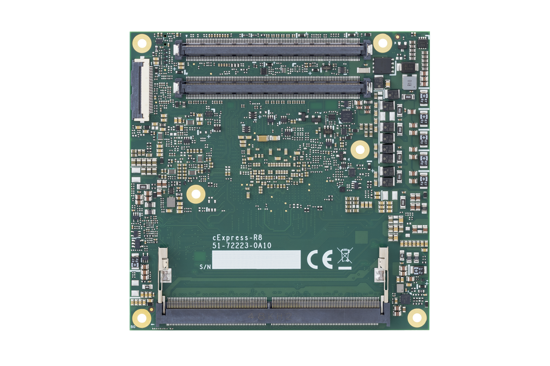
ADLINK Technology Inc., a global leader in edge computing solutions, introduces the cExpress-R8, a COM Express® COM.0 R3.1 Type 6 Compact module powered by AMD Ryzen™ Embedded 8000 Series processors (8845HS, 8840U, 8645HS, 8640U). Engineered to satisfy the demands of modern smart industrial applications, it delivers an advanced integration of high-performance and energy-efficient design. This module ignites mission-critical AI capabilities, accelerated edge computing, and advanced graphics performance — bringing the confidence that comes with the reliability needed for complex, graphics-intensive workloads.
Key Features:
AMD Ryzen™ Embedded 8000 Series Processors
AMD RDNA™ 3 Graphics and XDNA™ NPU (up to 40 TOPS performance)
Up to 96GB DDR5 5600 MT/s (ECC/non-ECC)
Four independent display outputs
Pushing the limits of edge performance, ADLINK’s cExpress-R8 combines up to 8 “Zen 4” cores and 16 threads with integrated AMD RDNA™ 3 graphics and an XDNA™ NPU, delivering up to 40 TOPS. The cExpress-R8 fuels power-efficient AI inferencing and fast decision-making across machine vision, robotics, medical imaging, infotainment, and intelligent human-machine systems. With XDNA™ architecture, performance-per-watt efficiency is optimized, delivering advanced AI processing, and enabling more complex AI workloads without a significant spike in energy demands.
To guarantee real-time processing, the cExpress-R8 supports up to 96GB of DDR5 memory at 5600 MT/s, with both ECC and non-ECC options available. ECC acts as a watchdog, detecting and correcting errors in environments, where failure isn’t an option, whether in mission-critical applications, gaming, transportation, and POS (Point of Sale)/POI (Point of Information) systems.
With support for up to four displays, DP, eDP, HDMI, LVDS, and VGA interfaces. VGA and eDP outputs are available as optional features, allowing flexible visual configurations to meet edge computing demands. Combined with scalable performance, power, and graphics configurations, the cExpress-R8 is well-suited for a diverse range of edge applications. With 10-year product availability, it ensures long-term design stability and lifecycle alignment for system integrator roadmaps.
ADLINK’s cExpress development kits, including reference carriers and full I/O support, will be available in Q4 of 2025 to help you accelerate prototyping and simplify system integration.