AOI in PCB & PCBA Manufacturing Process of PCBGOGO
PCB assembly consists of many steps. For PCBs with through-hole components, the assembly is quite easy.
PCB assembly consists of many steps. For PCBs with through-hole components, the assembly is quite easy. But for SMT components, elements are placed on the conductive pads with previously applied solder paste that holds the SMT parts together. Then the components are soldered to the pads. Due to the ever-growing demand for high-density circuit boards and smaller SMT components, defects during the PCB fabrication process increase. Thus, a thorough inspection is necessary at many stages of the fabrication process. PCBGOGO is a leading specialist in surface-mount, thru-hole, and mixed technology PCB assembly and electronic manufacturing services, as well as turn-key electronic PCB assembly. PCBGOGO is highly specialized not only in quick-turn PCB prototype and PCB assembly, but also medium and small volume PCB fabrication.
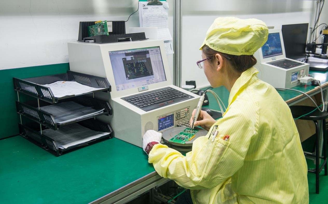
The assembly process at PCBGOGO consists of various inspection and functional verification stages to ensure that the requirements are completely satisfied. During the initial PCB manufacturing process, all the components are inspected by their IQC Department. Before chips are mounted on the PCB, IC programming service is also present. It is usually done by using a computer as a bridge for IC programming. After assembly, functional testing is done by software to ensures that the requirements are satisfied by the application. At PCBGOGO, all PCBs are tested for quality and correctness before shipping.
PCBGOGO team says,
“We guarantee that all our PCB products meet industry standards and undergo rigorous testing before delivery.”
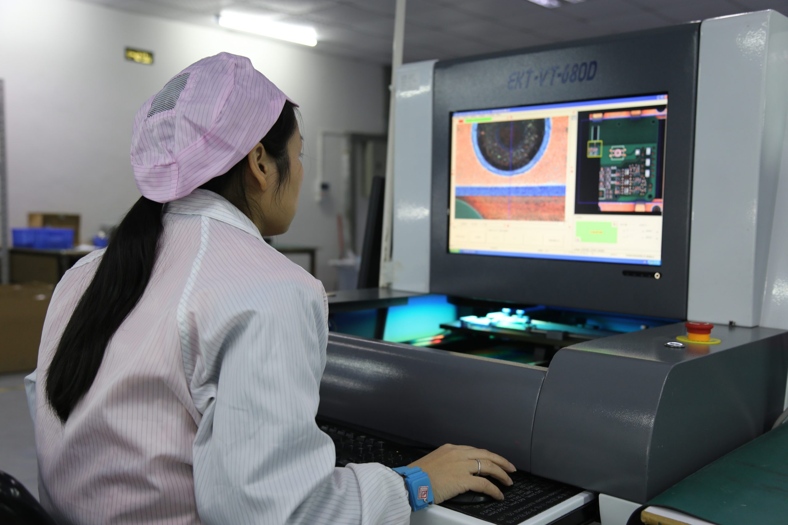
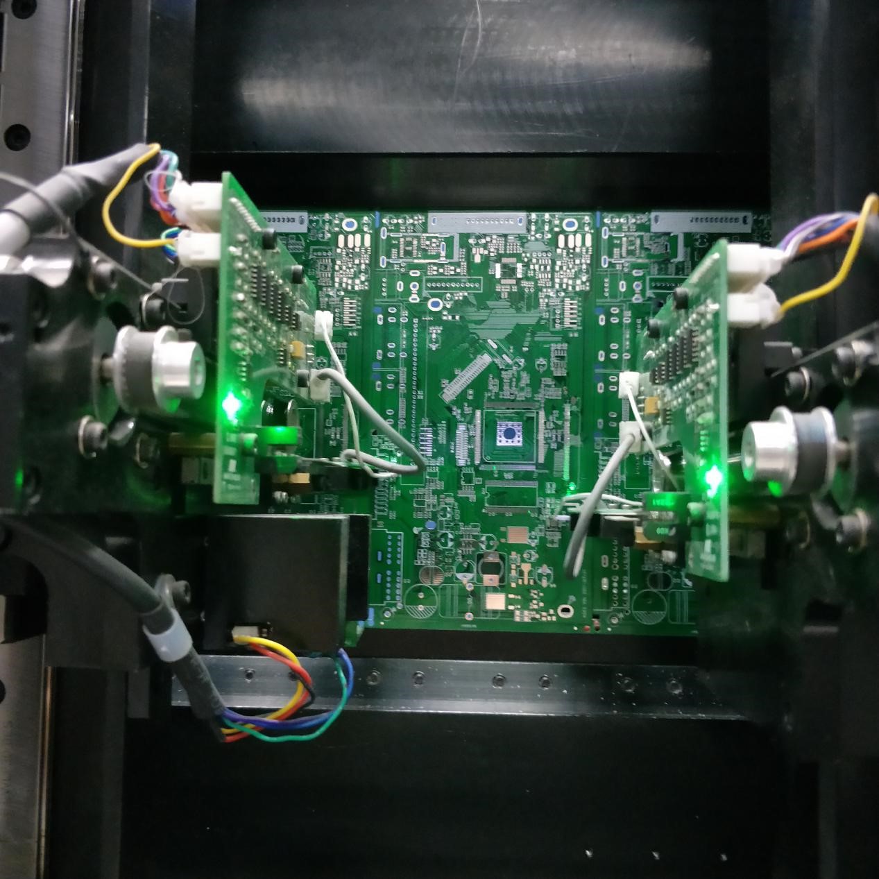
During PCB fabrication, AOI (Automated Optical Inspection) is a crucial process. It ensures that the PCBs leaving the production line are without any manufacturing defects. This inspection is used in PCB fabrication and PCB assembly, as well as testing printed circuit boards.
What is AOI?
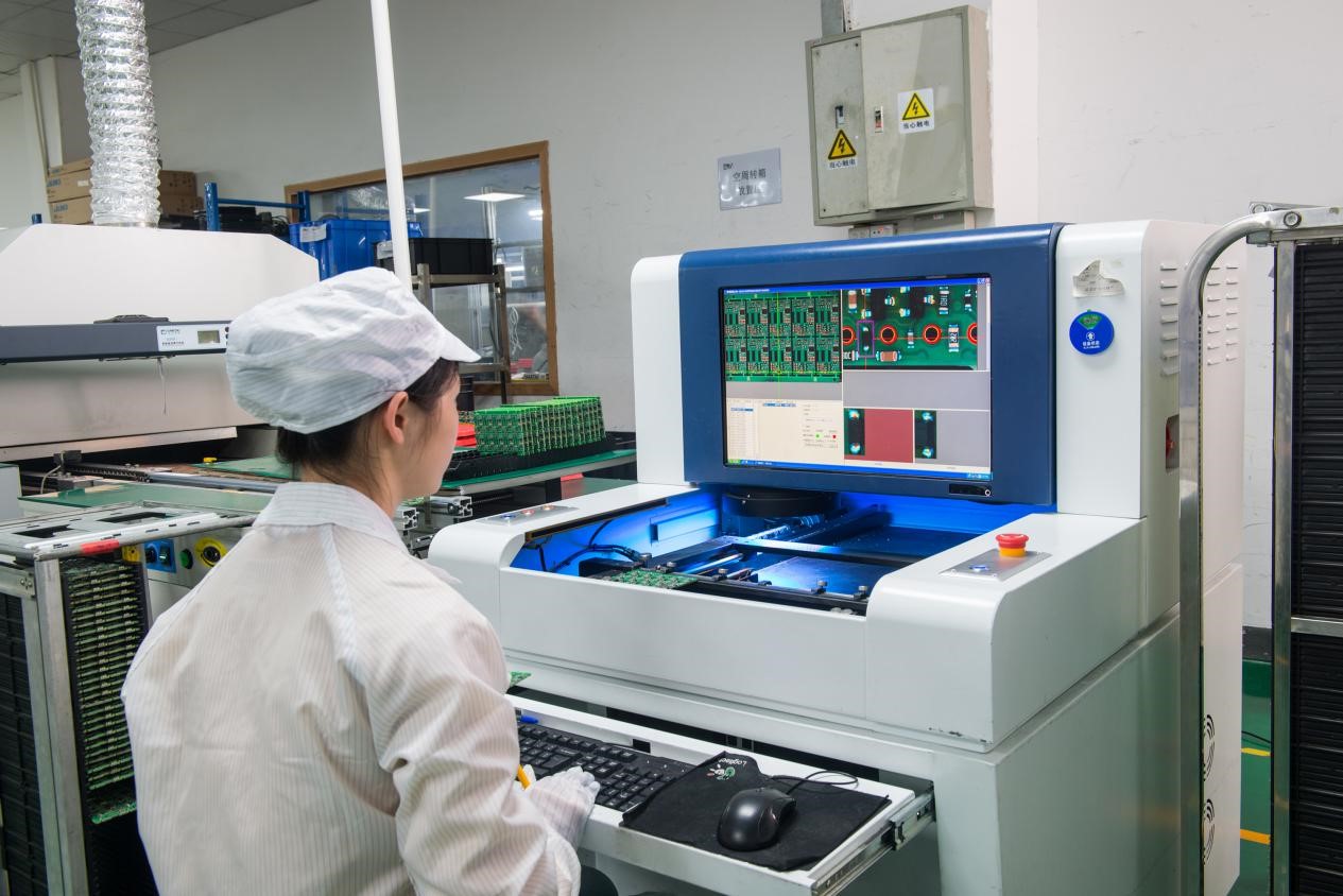
Automated optical inspection (AOI) is an automated visual inspection technique for printed circuit board manufacturing where a camera autonomously scans the device under test for both catastrophic failures and quality defects. The inspection technique can detect faults like missing components, components skew, surface defects, dimensional defects, etc. AOI is a machine-based technique as the accuracy required for the inspection is impossible via manual checking. This inspection tool increases the product quality in the production line at a low cost.
Compared to the traditional manual inspection method where technicians need to look at every component and mark them one by one, the AOI inspection method offers high accuracy. Moreover, the manual inspection is time-consuming work, whereas AOI only needs one minute to run through the whole board. Thus, AOI inspection method is accurate, reduce labor cost and time cost greatly.
AOI offers various advantages like:
- High Accuracy
- Tunability (adaptability according to the needs of the assembled PCBs)
- High efficiency: AOI only needs one minute to run through the whole board, which can reduce labor cost and time cost greatly
- It is cost-effective as compared to automatic X-ray inspection.
- It can also detect aspects such as component soldering, polarity, and values.
AOI can detect the following component defects: insufficient solder joints, height defects, wrong part, solder bridging, excessive solder joints, billboarding, volume defects, tombstoning, component offset, component polarity, component presence or absence, component skew, area defects, flipped element, insufficient paste around leads, lifted leads, no population tests, paste registration, and severely damaged components.
Moreover, it can detect PCB defects such as short circuits, line width violations, spacing violations, excess copper, missing pad, cuts, incorrect mounting of components, and hole breakage.
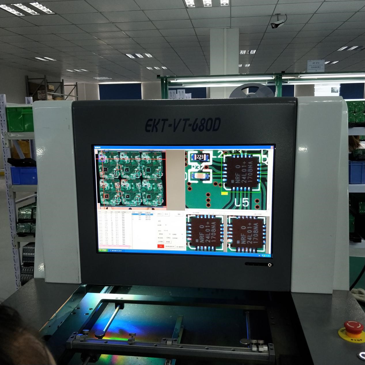
AOI at PCBGOGO
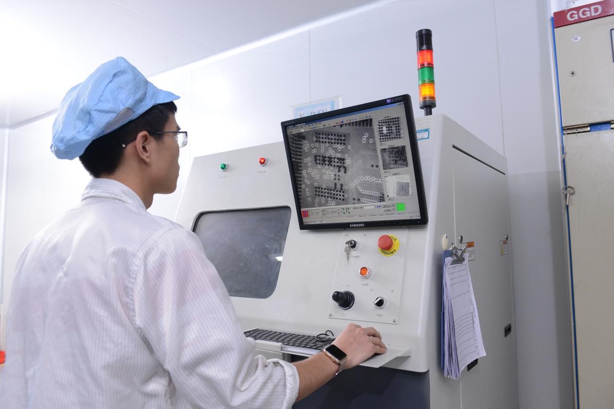
PCBGOGO owns advanced AOI equipment and software to meet the requirement for accuracy, speed, and production. PCBGOGO also provides X-ray inspection as one of the quality control steps. This method uses an X-ray system to find hidden defects without risking damage to the board. PCBGOGO team remarks,
“Automatic optical inspection and X-Ray inspection are necessary tools for the PCB fabrication industry. And we will be committed to adhering to the strictest standards in manufacture and assembly with AOI and X-Ray inspection.”
Other Quality Assurance Methods by PCBGOGO
PCBGOGO offers many quality assurance techniques besides AOI and X-ray inspection like Electrical Test (E-Test), Impedance Control, ROHS-lead free verification and UL certification. With more dense PCB designs, it is necessary to test the PCBs by one of the Electrical test methods to ensure that all vias are connected because AOI cannot find this issue. Only E-Test can check for the missing connections on the board.
The main electrical testing procedures for PCBs are listed as following:
- Circuits open and short testing
- Capacitance testing
- Resistance testing
- Comparative testing
- Flip testing
- Continuity testing
- Adjacency testing
Also, for high-frequency circuits, a controlled impedance is important. Impedance generally refers to the overall resistance, and it takes into account the effects of capacitance and inductance. Impedance testing is required to ensure that the impedance mismatches are within the allowable limits through some designs for the PCBs. If impedance mismatches are not limited, then the signal flowing through the traces gets reflected due to the mismatch in source and load impedance. As a result, only a fraction of the signal reaches the load and in the signal path, standing waves are created. Therefore, to maintain signal integrity, impedance control is critical. At PCBGOGO, impedance calculations are confirmed with the impedance values and tolerances provided by PCB designers before PCB manufacturing to achieve your expectations with the best quality.
Furthermore, PCBGOGO checks the product for RoHS compliance. RoHS refers to the restriction of hazardous substances. Restricting elements such as lead provides a safe manufacturing environment for the workers and safe products for the users. The PCBGOGO team says on their knowledge center,
“We play an active role in eliminating harmful substances in electronic products by providing PCB manufacturing and PCB assembly prototype services that comply with RoHS regulations.”
Overall, the PCBGOGO PCB services provide a complete suite including PCB prototype, PCB assembly, PCB small-batch manufacturing, and PCB testing in a short time and at a competitive price.
Besides, PCBGOGO offers PCB build time as fast as 2-3 days and can also provide 12 hours and 24 hours service for urgent projects.
Further information related to the AOI and other QC methods at PCBGOGO can be found here.


